
2016 Microchip Technology Inc.
DS20005611A-page 1
DSC2311
Features
• Two Simultaneous CMOS Outputs
- Output 1 Range: 2.3 MHz to 170 MHz
- Output 2 Range: 2.3 MHz to 170 MHz
• Low RMS Phase Jitter: <1 ps (typ.)
• High Stability: ±25 ppm, ±50 ppm
• Wide Temperature Range
- Automotive: –40
°
C to +125
°
C
- Ext. Industrial –40
°
C to +105
°
C
- Industrial –40
°
C to +85
°
C
- Ext. Commercial –20
°
C to +70
°
C
• High Supply Noise Rejection: –50 dBc
• High Shock and Vibration Immunity
- Qualified to MIL-STD-883
• High Reliability
- 20x higher MTBF than crystal-based clock
generator designs
• Supply Range of 2.25V to 3.6V
• Lead Free and RoHS-Compliant
Applications
• Consumer Electronics
• Camera and Imaging Modules
• Home Automation
• Industrial and Power Conversion
• Mobile Communications, Internet, and Sensor
Devices
• Solid State, Hard Drive, and Flash Drive Storage
General Description
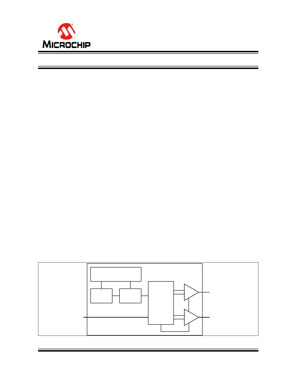
The DSC2311 is a crystal-less™ clock generator that is
factory-configurable to simultaneously output two
separate frequencies from 2.3 MHz to 170 MHz. The
clock generator uses proven silicon MEMS technology
to provide low jitter and high frequency stability across
a wide range of supply voltages and temperatures. By
eliminating the external quartz crystal, crystal-less
clock generators significantly enhance reliability and
accelerate product development, while meeting
stringent clock performance criteria for a variety of
consumer electronics, communications, and storage
applications.
DSC2311 has an Output Enable/Disable feature that
allows it to disable the outputs when OE is low. The
device is available in a space-saving 6-pin 2.5 mm x
2.0 mm crystal-less VDFN package that uses only a
single external bypass capacitor. This requires a PCB
footprint equivalent to that of a 1.0 mm x 1.0 mm
crystal-based clock generator.
Block Diagram
Control Circuitry
MEMS
PLL
Output
Control
and
Divider
F
OUT2
F
OUT1
OE
Crystal-less™ Configurable Two-Output Clock Generator
DSC2311
DS20005611A-page 2
2016 Microchip Technology Inc.
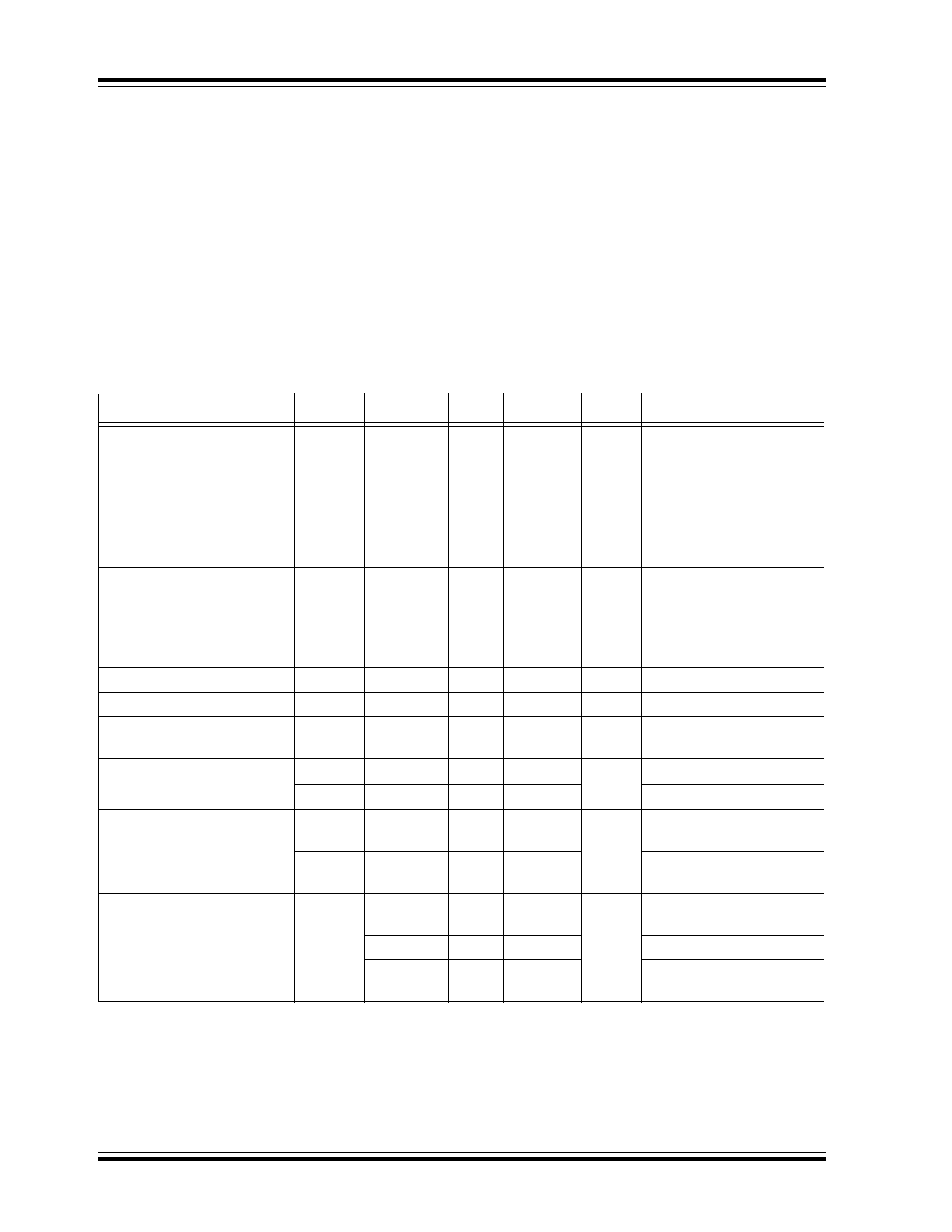
1.0
ELECTRICAL CHARACTERISTICS
Absolute Maximum Ratings †
Supply Voltage .......................................................................................................................................... –0.3V to +4.0V
Input Voltage .......................................................................................................................................–0.3V to V
DD
+0.3V
ESD Protection (HBM) ...............................................................................................................................................4 kV
ESD Protection (CDM) ............................................................................................................................................1.5 kV
†
Notice: Stresses above those listed under “Absolute Maximum Ratings” may cause permanent damage to the device.
This is a stress rating only and functional operation of the device at those or any other conditions above those indicated
in the operational sections of this specification is not intended. Exposure to maximum rating conditions for extended
periods may affect device reliability.
ELECTRICAL CHARACTERISTICS
Specifications: V
DD
= 3.3V; T
A
= +25°C unless otherwise specified.
Parameters
Sym.
Min.
Typ.
Max.
Units
Conditions
Supply Voltage (
Note 1
)
V
DD
2.25
—
3.6
V
—
Supply Current (
Note 2
)
I
DD
—
21
23
mA
EN pin low. All outputs
disabled.
Frequency Stability (
Note 3
)
∆f
—
—
±25
ppm
Includes frequency
variations due to initial
tolerance, temperature, and
power supply voltage.
—
—
±50
Aging
∆f
—
—
±5
ppm
One year at +25
°
C
Start-up Time (
Note 4
)
t
SU
—
—
5
ms
T = +25
°
C
Input Logic Levels
V
IH
0.75 x V
DD
—
—
V
Input logic high
V
IL
—
—
0.25 x V
DD
Input logic low
Output Disable Time
t
DA
—
—
5
ns
—
Output Enable Time
t
EN
—
—
20
ns
—
Pull-Up Resistor (
Note 2
)
—
—
40
—
kΩ
Pull-up exists on all digital
IO
Output Logic Levels
V
OH
0.9 x V
DD
—
—
V
Output logic high, I = ±6 mA
V
OL
—
—
0.1 x V
DD
Output logic low, I = ±6 mA
Output Transition Time
t
R
—
1.1
2.0
ns
Rise time. 20% to 80%;
C
L
= 15 pF
t
F
—
1.4
2.0
Fall time. 20% to 80%;
C
L
= 15 pF
Frequency
f
0
2.3
—
170
MHz
Commercial/Industrial temp.
range
3.3
—
100
Automotive temp. range
3.3
—
170
Extended Industrial temp.
range
Note 1:
Pin 4 V
DD
should be filtered with a 0.01 µF capacitor.
2:
Output is enabled if Enable pad is floated or not connected. Operating current = disabled current + ∆I
DD
from F
OUT1
+ ∆I
DD
from F
OUT2
. See
Current Consumption
graph for more information.
3:
For other ppm stabilities, please contact the factory.
4:
t
SU
is time to 100 ppm stable output frequency after V
DD
is applied and outputs are enabled.
5:
Period jitter includes crosstalk from adjacent output.
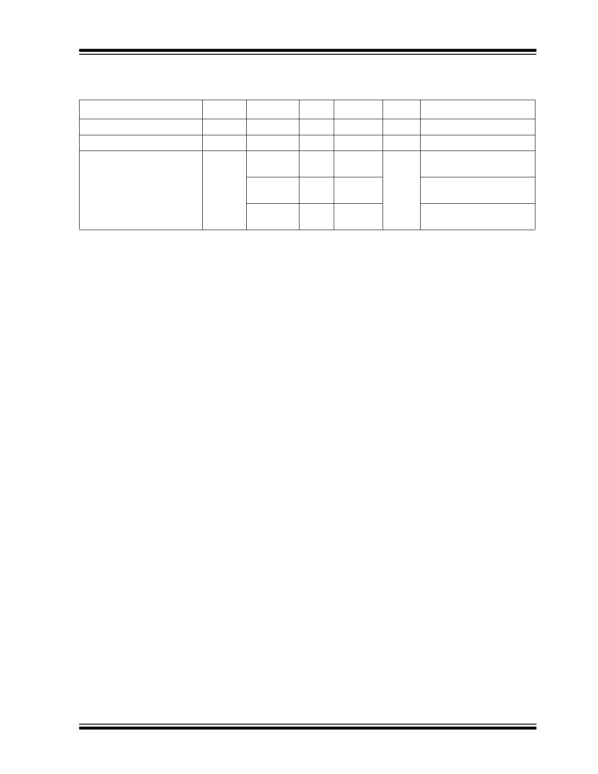
2016 Microchip Technology Inc.
DS20005611A-page 3
DSC2311
Output Duty Cycle
SYM
45
—
55
%
—
Period Jitter (
Note 5
)
J
PER
—
3
—
ps
RMS
F
O1
= F
O2
= 25 MHz
Integrated Phase Noise
J
CC
—
0.3
—
ps
RMS
200 kHz to 20 MHz @
25 MHz
—
0.38
—
100 kHz to 20 MHz @
25 MHz
—
1.7
2
12 kHz to 20 MHz @
25 MHz
ELECTRICAL CHARACTERISTICS (CONTINUED)
Specifications: V
DD
= 3.3V; T
A
= +25°C unless otherwise specified.
Parameters
Sym.
Min.
Typ.
Max.
Units
Conditions
Note 1:
Pin 4 V
DD
should be filtered with a 0.01 µF capacitor.
2:
Output is enabled if Enable pad is floated or not connected. Operating current = disabled current + ∆I
DD
from F
OUT1
+ ∆I
DD
from F
OUT2
. See
Current Consumption
graph for more information.
3:
For other ppm stabilities, please contact the factory.
4:
t
SU
is time to 100 ppm stable output frequency after V
DD
is applied and outputs are enabled.
5:
Period jitter includes crosstalk from adjacent output.
DSC2311
DS20005611A-page 4
2016 Microchip Technology Inc.
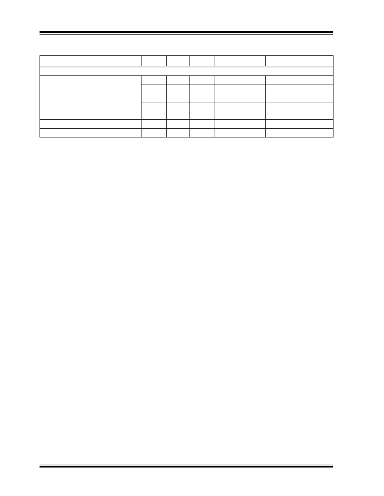
TEMPERATURE SPECIFICATIONS (
Note 1
)
Parameters
Sym.
Min.
Typ.
Max.
Units
Conditions
Temperature Ranges
Operating Temperature Range (T)
T
A
–20
—
+70
°C
Ordering Option E
T
A
–40
—
+85
°C
Ordering Option I
T
A
–40
—
+105
°C
Ordering Option L
T
A
–40
—
+125
°C
Ordering Option M
Junction Temperature
T
J
—
—
+150
°C
—
Storage Temperature Range
T
S
–40
—
+150
°C
—
Soldering Temperature Range
—
—
—
+260
°C
40 sec. max.
Note 1:
The maximum allowable power dissipation is a function of ambient temperature, the maximum allowable
junction temperature, and the thermal resistance from junction to air (i.e., T
A
, T
J
,
JA
). Exceeding the
maximum allowable power dissipation will cause the device operating junction temperature to exceed the
maximum +125°C rating. Sustained junction temperatures above +125°C can impact the device reliability.
2016 Microchip Technology Inc.
DS20005611A-page 5
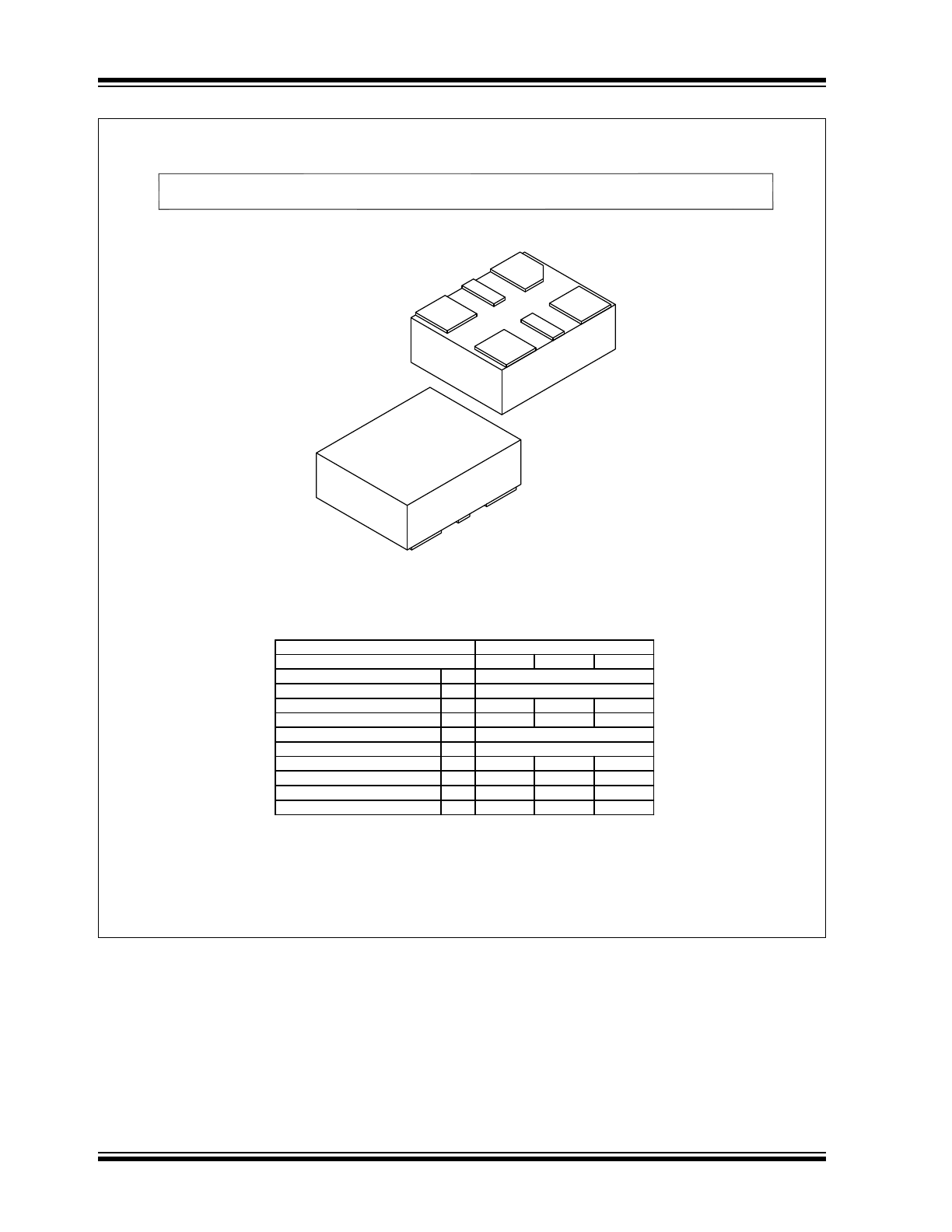
DSC2311
2.0
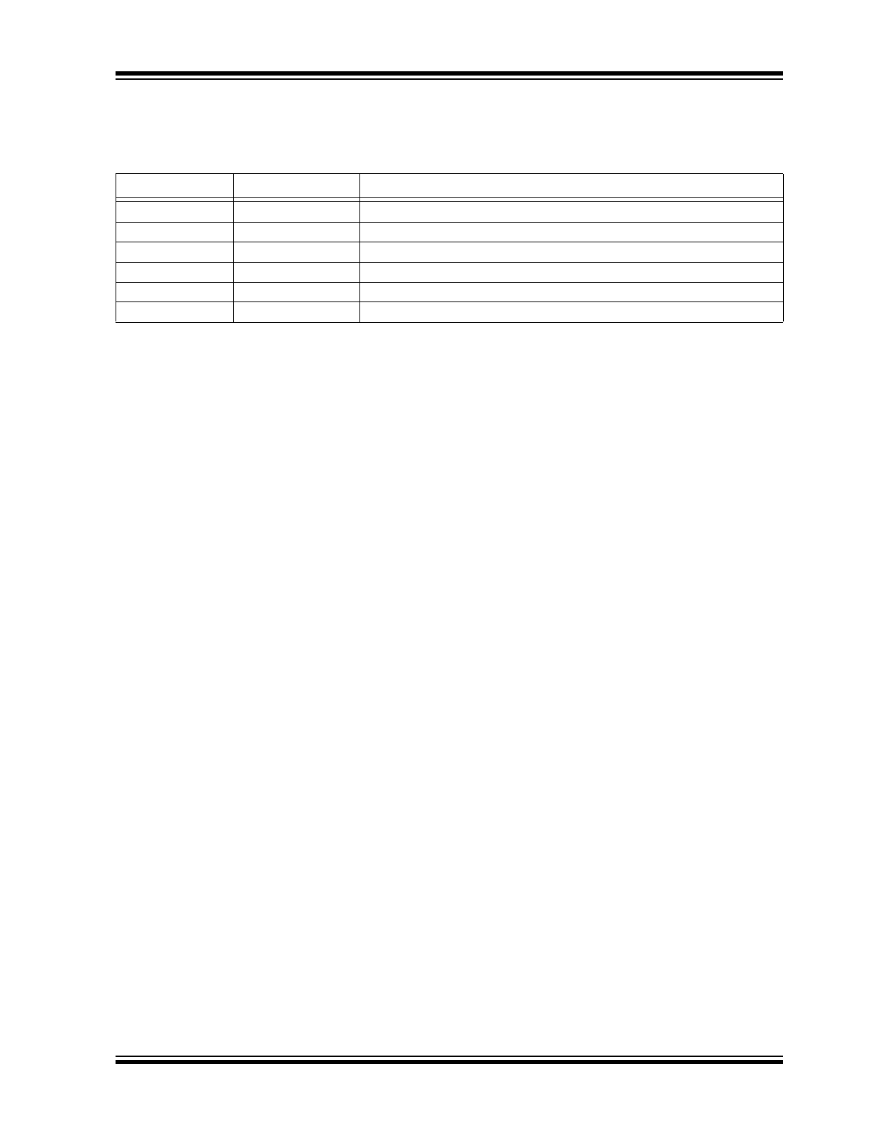
PIN DESCRIPTIONS
The descriptions of the pins are listed in
Table 2-1
.
TABLE 2-1:
PIN FUNCTION TABLE
Pin Number
Pin Name
Description
1
ENABLE
Output Enable for both CLK0 and CLK1.
2
N/C
Do not connect.
3
GROUND
Ground.
4
CLK0
Clock Output 0 (CMOS).
5
CLK1
Clock Output 1 (CMOS).
6
VDD
Supply Voltage.
DSC2311
DS20005611A-page 6
2016 Microchip Technology Inc.
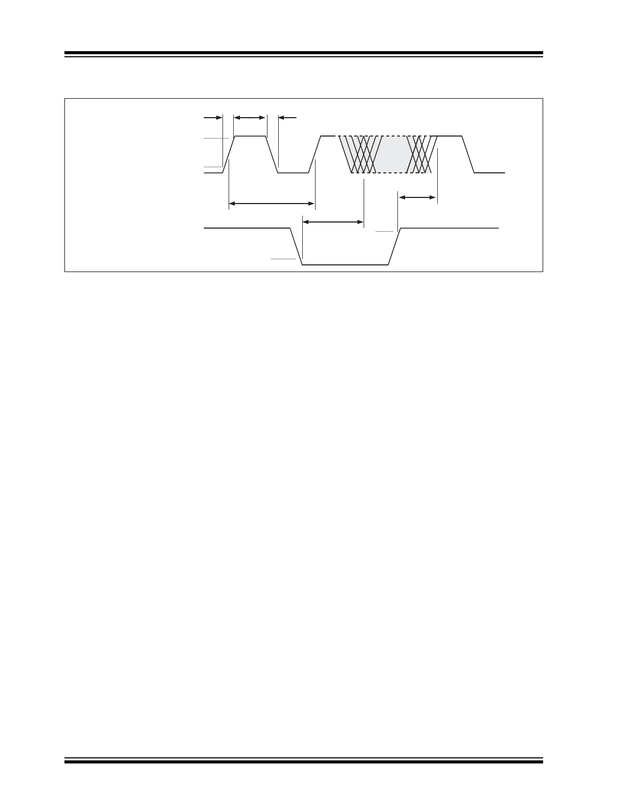
3.0
OUTPUT WAVEFORM
FIGURE 3-1:
OE Function and Output Waveform: LVCMOS.
V
OH
V
OL
V
IL
1/f
o
Output
Enable
t
DA
t
EN
t
F
t
R
V
IH
2016 Microchip Technology Inc.
DS20005611A-page 7
DSC2311
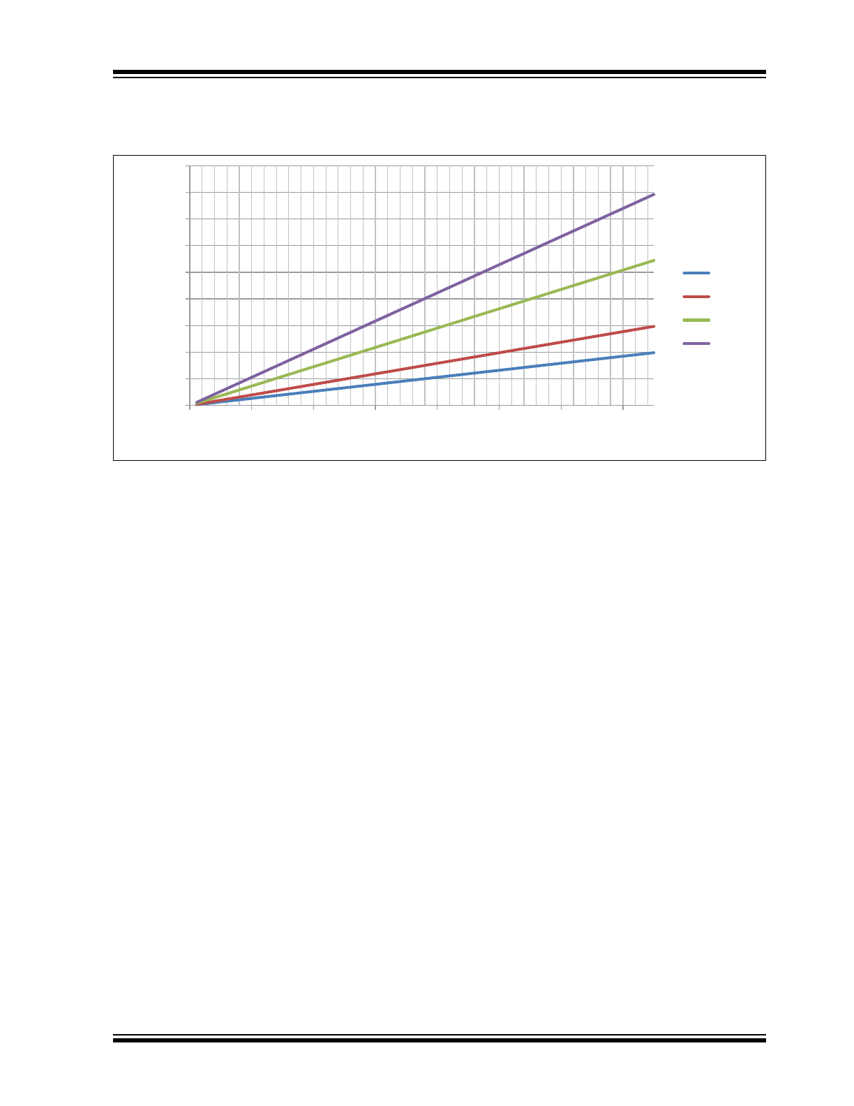
4.0
CURRENT CONSUMPTION
Total Current = Disabled Current + ∆I
DD
F
OUT1
+ ∆I
DD
F
OUT2
FIGURE 4-1:
∆I
DD
/ Output vs. Frequency and Load @ 3.3V V
DD
3 pF
5 pF
10 pF
15 pF
F
OUT
(MHz)
ΔI
DD
(mA)
0 20 40 60 80 100 120 140
18
16
14
12
10
8
6
4
2
0
DSC2311
DS20005611A-page 8
2016 Microchip Technology Inc.
5.0
SOLDER REFLOW PROFILE
260°C
217°C
200°C
150°C
25°C
TEMPERA
T
URE (°C)
8 MINUTES MAX.
3°C/SEC. MAX.
3°C/SEC. MAX.
PRE-HEAT
REFLOW
COOL
TIME
60-180
SECONDS
60-150
SECONDS
20-40
SECONDS
6°C/SEC. MAX.
6-PIN QFN MSL 1 @ 260°C refer to JSTD-020C
Ramp-Up Rate (200°C to Peak Temp)
3°C/sec. max.
Preheat Time 150°C to 200°C
60-180 sec.
Time Maintained above 217°C
60-150 sec.
Peak Temperature
255°C to 260°C
Time within 5°C of Actual Peak
20-40 sec.
Ramp-Down Rate
6°C/sec. max.
Time 25°C to Peak Temperature
8 minutes max.
2016 Microchip Technology Inc.
DS20005611A-page 9
DSC2311
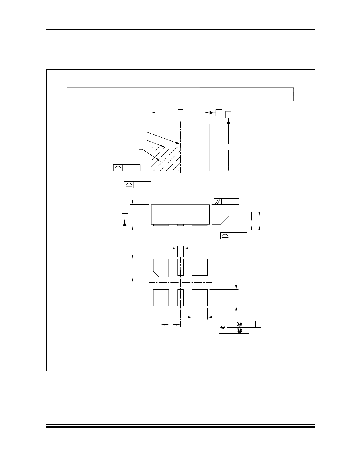
6.0
PACKAGE MARKING INFORMATION
6-Lead VDFN 2.5 mm x 2.0 mm Package Outline and Recommended Land Pattern
B
A
0.05 C
0.05 C
(DATUM B)
(DATUM A)
C
SEATING
PLANE
1
N
2X
TOP VIEW
SIDE VIEW
NOTE 1
0.10 C
0.08 C
Microchip Technology Drawing C04-1005A Sheet 1 of 2
2X
6X
For the most current package drawings, please see the Microchip Packaging Specification located at
http://www.microchip.com/packaging
Note:
6-Lead Very Thin Dual Flatpack No-Leads (J7A) - 2.5x2.0 mm Body [VDFN]
D
E
A
A1
0.10
C A B
0.05
C
BOTTOM VIEW
1
2
N
2X b2
4X b1
5X L1
L2
e
2
DSC2311
DS20005611A-page 10
2016 Microchip Technology Inc.
REF: Reference Dimension, usually without tolerance, for information purposes only.
BSC: Basic Dimension. Theoretically exact value shown without tolerances.
1.
2.
3.
Notes:
Pin 1 visual index feature may vary, but must be located within the hatched area.
Package is saw singulated
Dimensioning and tolerancing per ASME Y14.5M
For the most current package drawings, please see the Microchip Packaging Specification located at
http://www.microchip.com/packaging
Note:
Microchip Technology Drawing C04-1005A Sheet 2 of 2
6-Lead Very Thin Dual Flatpack No-Leads (J7A) - 2.5x2.0 mm Body [VDFN]
Number of Terminals
Overall Height
Terminal Width
Overall Width
Terminal Length
Pitch
Standoff
Units
Dimension Limits
A1
A
b1
e
L2
E
N
0.825 BSC
0.665
0.60
0.80
0.00
0.65
0.765
0.85
0.02
2.00 BSC
MILLIMETERS
MIN
NOM
6
0.865
0.70
0.90
0.05
MAX
Overall Length
D
2.50 BSC
Terminal Length
L1
0.60
0.70
0.80
Terminal Width
b2
0.20
0.25
0.30