
2016 Microchip Technology Inc.
DS20005612A-page 1
DSC400
Features
• Low RMS Phase Jitter: <1 ps (typ.)
• High Stability: ±25 ppm, ±50 ppm
• Wide Temperature Range:
- Industrial –40°C to +85°C
- Ext. Commercial –20°C to +70°C
• High Supply Noise Rejection: –50 dBc
• Four Format-Configurable Outputs:
- LVPECL, LVDS, HCSL, LVCMOS
• Available Pin-Selectable Frequency Table
- 1 Pin per Bank for 2 Frequency Sets
• Wide Frequency Range:
- 2.3 MHz – 460 MHz
• 20-Pin QFN Footprint (5.0 mm x 3.2 mm)
• Excellent Shock and Vibration Immunity
• High Reliability
- 20x better MTF than quartz-based devices
• Wide Supply Range of 2.25V to 3.6V
• Lead Free and RoHS-Compliant
• AEC-Q100 Automotive Qualified
Applications
• Communications and Networks
• Ethernet
- 1G, 10GBASE-T/KR/LR/SR, and FCoE
• Storage Area Networks
- SATA, SAS, Fibre Channel
• Passive Optical Networks
- EPON, 10G-EPON, GPON, 10G-PON
• HD/SD/SDI Video and Surveillance
• Automotive
• Media and Video
• Embedded and Industrial
General Description
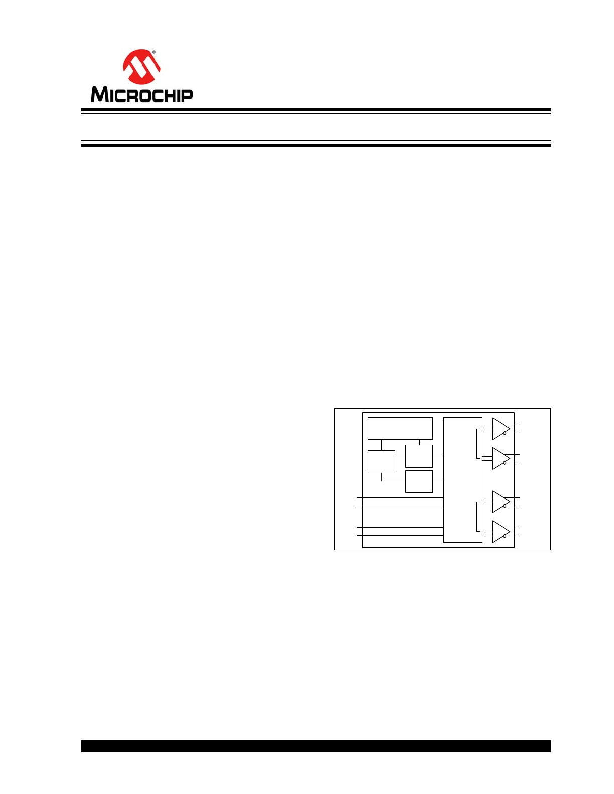
The DSC400 is a four output crystal-less™ clock
generator. It utilizes proven PureSilicon™ MEMS
technology to provide excellent jitter and stability while
incorporating additional device functionality.
The nominal frequencies of the outputs can be identical
or independently derived from common PLLs.
Each output may be configured independently to
support a single-ended LVCMOS interface or a
differential interface. Differential options include
LVPECL, LVDS, or HCSL.
The DSC400 provides two independent select lines for
choosing between two sets of pre-configured
frequencies per bank. It also has two OE pins to allow
for enabling and disabling outputs.
The DSC400 is packaged in a 20-pin QFN (5 mm x
3.2 mm) and is available in extended commercial and
industrial temperature grades.
Block Diagram
CLK0+
BANK 2
OUTPUT
CONTROL
AND
DIVIDERS
CONTROL
CIRCUITRY
MEMS
PLL
OE1
OE2
FSB1
FSB2
BANK 1
CLK0-
CLK3+
CLK3-
CLK1+
CLK1-
CLK2+
CLK2-
PLL
Configurable Four Output, Low Jitter Crystal-less™ Clock Generator
DSC400
DS20005612A-page 2
2016 Microchip Technology Inc.
1.0
ELECTRICAL CHARACTERISTICS
Absolute Maximum Ratings †
Supply Voltage .......................................................................................................................................... –0.3V to +4.0V
Input Voltage .......................................................................................................................................–0.3V to V
DD
+0.3V
ESD Protection (HBM) ...............................................................................................................................................4 kV
ESD Protection (MM) ................................................................................................................................................400V
ESD Protection (CDM) ............................................................................................................................................1.5 kV
†
Notice: Stresses above those listed under “Absolute Maximum Ratings” may cause permanent damage to the device.
This is a stress rating only and functional operation of the device at those or any other conditions above those indicated
in the operational sections of this specification is not intended. Exposure to maximum rating conditions for extended
periods may affect device reliability.
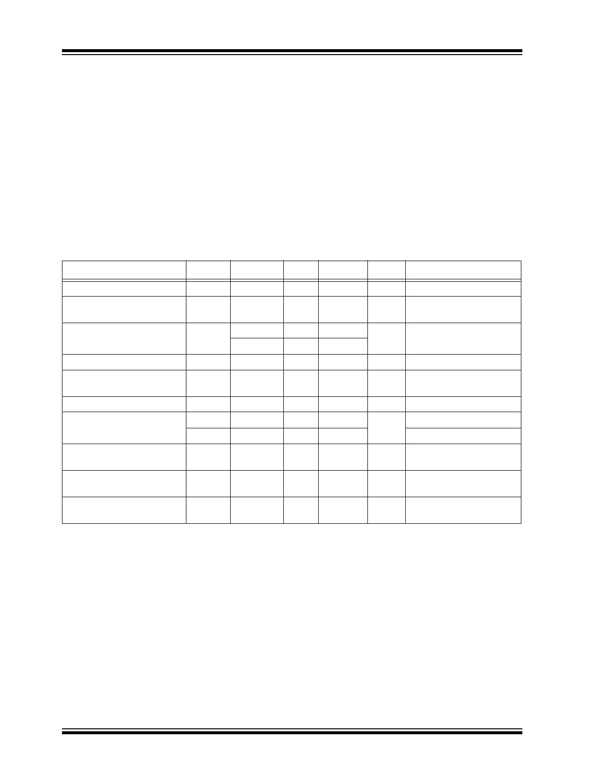
ELECTRICAL CHARACTERISTICS
Specifications: V
DD
= 3.3V; T
A
= +25°C unless otherwise specified.
Parameters
Sym.
Min.
Typ.
Max.
Units
Conditions
Supply Voltage (
Note 1
)
V
DD
2.25
—
3.6
V
—
Core Supply Current (
Note 2
)
I
DDCORE
—
40
44
mA
OE(1:2) = 0. All outputs
disabled.
Frequency Stability
∆f
—
—
±25
ppm
All temperature and V
DD
ranges.
—
—
±50
Aging - First Year
∆f
Y1
—
—
±5
ppm
One year at +25°C
Aging - After First Year
∆f
Y2
+
—
—
<±1
ppm/yr Year two and beyond at
+25°C
Start-up Time (
Note 3
)
t
SU
—
—
5
ms
T = +25°C
Input Logic Levels
V
IH
0.75 x V
DD
—
—
V
Input logic high
V
IL
—
—
0.25 x V
DD
Input logic low
Output Disable Time (
Note 4
)
t
DA
—
—
5
ns
OE(1:2) transition
from 1 to 0
Output Enable Time (
Note 4
)
t
EN
—
—
20
ns
OE(1:2) transition
from 0 to 1
Pull-Up Resistor
R
PU
—
40
—
kΩ
All input pins have an
internal pull-up
Note 1:
V
DD
pins should be filtered with a 0.1 µF capacitor connected between V
DD
and V
SS
.
2:
The addition of I
DDCORE
and I
DDIO
provides the total current consumption of the device.
3:
t
SU
is time to 100 ppm stable output frequency after V
DD
is applied and outputs are enabled.
4:
See the
Output Waveform
section for more information.
2016 Microchip Technology Inc.
DS20005612A-page 3
DSC400
TEMPERATURE SPECIFICATIONS (
Note 1
)
Parameters
Sym.
Min.
Typ.
Max.
Units
Conditions
Temperature Ranges
Operating Temperature Range (T)
T
A
–20
—
+70
°C
Ordering Option E
T
A
–40
—
+85
°C
Ordering Option I
Junction Temperature
T
J
—
—
+150
°C
—
Storage Temperature Range
T
S
–40
—
+150
°C
—
Soldering Temperature
—
—
—
+260
°C
40 sec. max.
Note 1:
The maximum allowable power dissipation is a function of ambient temperature, the maximum allowable
junction temperature, and the thermal resistance from junction to air (i.e., T
A
, T
J
,
JA
). Exceeding the
maximum allowable power dissipation will cause the device operating junction temperature to exceed the
maximum +125°C rating. Sustained junction temperatures above +125°C can impact the device reliability.
DSC400
DS20005612A-page 4
2016 Microchip Technology Inc.
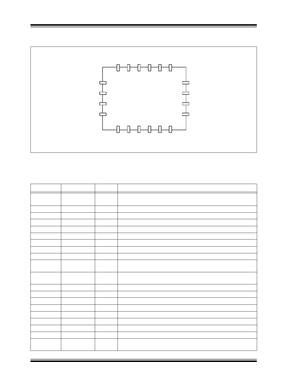
2.0
PIN DESCRIPTIONS
FIGURE 2-1:
Pin Configuration, 20-Pin QFN (5.0 mm x 3.2 mm)
The descriptions of the pins are listed in
Table 2-1
.
TABLE 2-1:
PIN FUNCTION TABLE
Pin Number
Pin Name
Pin Type
Description
1
OE1
I
Output Enable for Bank1 (CLK0 and CLK3); Active-High. See
Table 3-1
.
2
NC
N/A
Leave unconnected or connect to ground.
3
V
SS
PWR
Ground.
4
V
SS
PWR
Ground.
5
CLK0–
O
Complement output of differential pair 0 (off when in LVCMOS format).
6
CLK0+
O
True output of differential pair 0 or LVCMOS output 0.
7
CLK1–
O
Complement output of differential pair 1 (off when in LVCMOS format).
8
CLK1+
O
True output of differential pair 1 or LVCMOS output 1.
9
V
DD2
PWR
Power Supply for Bank2 (CLK1 and CLK2).
10
FSB2
I
Input for selecting pre-configured frequencies on Bank2 (CLK1 and
CLK2).
11
OE2
I
Output Enable for Bank2 (CLK1 and CLK2); Active-High. See
Table 3-1
.
12
NC
N/A
Leave unconnected or connect to ground.
13
V
SS
PWR
Ground.
14
V
SS
PWR
Ground.
15
CLK2–
O
Complement output of differential pair 2 (off when in LVCMOS format).
16
CLK2+
O
True output of differential pair 2 or LVCMOS output 2.
17
CLK3–
O
Complement output of differential pair 3 (off when in LVCMOS format).
18
CLK3+
O
True output of differential pair 3 or LVCMOS output 3.
19
V
DD1
PWR
Power Supply for Bank1 (CLK0 and CLK3).
20
FSB1
I
Input for selecting pre-configured frequencies on Bank1 (CLK0 and
CLK3).
OE2
11
NC
VSS
VSS
13
12
14
VSS
4
VSS
NC
OE1
2
3
1
CLK
0-
5
CLK
0+
CLK
1-
CLK
1+
VD
D
2
FS
B
2
7
6
8
9
10
CLK
2-
15
CLK
2+
CLK
3-
CLK
3+
VD
D
1
FS
B
1
17
16
18
19
20
2016 Microchip Technology Inc.
DS20005612A-page 5
DSC400
3.0
OPERATIONAL DESCRIPTION
The DSC400 is a crystal-less™ clock generator. Unlike
older clock generators in the industry, it does not
require an external crystal to operate; it relies on the
integrated MEMS resonator that interfaces with internal
PLLs. This technology enhances performance and
reliability by allowing tighter frequency stability over a
far wider temperature range. In addition, the higher
resistance to shock and vibration decreases the aging
rate to allow for much improved product life in the
system.
3.1
Inputs
There are four input signals in the device. Each has an
internal (40 kΩ) pull-up to default the selection to a high
(1). Inputs can be controlled through hardware
strapping method with a resistor to ground to assert the
input low (0). Inputs may also be controlled by other
components’ GPIOs
In case more than one frequency set is desired, FSB1
and FSB2 are used to independently select one of two
sets per bank. FSB1 selects the pre-configured set on
Bank1 (CLK0 and CLK3) and FSB2 selects the
pre-configured set on Bank2 (CLK1 and CLK2), as
shown in
Table 1-1
in the
Product Identification System
section.
If there is a requirement to disable outputs, the inputs
OE1 and OE2 are used in conjunction to disable the
banks of outputs. Outputs are disabled in tri-state (Hi-Z)
mode. See
Table 3-1
for more information.
3.2
Outputs
The four outputs are grouped into two banks. Each
bank is supplied by an independent V
DD
to allow for
optimized noise isolation between the two banks. Each
bank provides two synchronous outputs generated by
a common PLL:
• Bank1 is composed of outputs CLK0 and CLK3.
• Bank2 is composed of outputs CLK1 and CLK2.
Each output may be pre-configured independently to
be one of the following formats: LVCMOS, LVDS,
LVPECL or HCSL. In case the output is configured to
be single-ended LVCMOS, the frequency is generated
on the true output (CLKx+) and the complement output
(CLKx–) is shut off in a low state. Frequencies can be
chosen from 2.3 MHz to 460 MHz for differential
outputs and from 2.3 MHz to 170 MHz on LVCMOS
outputs.
3.3
Power
V
DD1
and V
DD2
supply the power to banks 1 and 2
respectively. Each V
DD
may each have a different
supply voltage from the other as long as it is within the
2.25V to 3.6V range. Each V
DD
pin should have a
0.1 µF capacitor to filter high-frequency noise. V
SS
is
common to the entire device.
TABLE 3-1:
OUTPUT ENABLE
SELECTION TABLE
OE1
OE2
Bank 1
(CLK0 & CLK3)
Bank 2
(CLK1 & CLK2)
0
0
Hi-Z
Hi-Z
0
1
Hi-Z
Running
1
0
Running
Hi-Z
1
1
Running
Running
DSC400
DS20005612A-page 6
2016 Microchip Technology Inc.
4.0
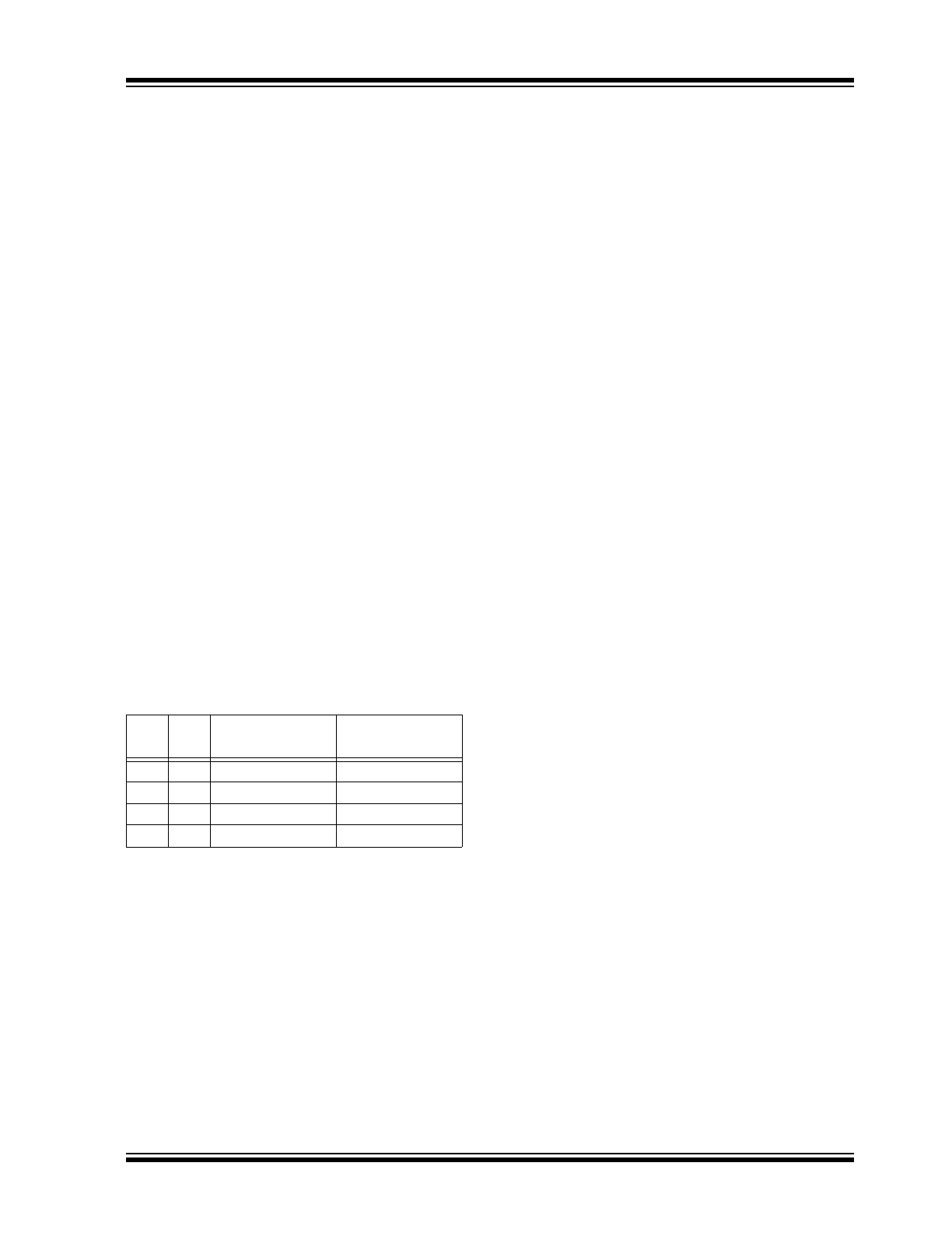
TERMINATION SCHEMES
4.1
LVPECL
FIGURE 4-1:
Typical LVPECL Termination Scheme.
Note 1:
LVPECL applicable to extended commercial temperature only.
2:
See the
Output Waveform
section for more information.
3:
The addition of I
DDCORE
and I
DDIO
provides the total current consumption of the device.
4:
Period jitter includes crosstalk from adjacent output.
V
DD
100 Ω
130 Ω
82 Ω
130 Ω
82 Ω
TABLE 4-1:
LVPECL OUTPUTS (
Note 1
)
Parameter
Symbol
Min.
Typ.
Max.
Units
Condition
Output Logic
Levels
V
OH
V
DD
– 1.08
—
—
V
Output Logic High, R
L
= 50Ω to V
DD
–2V
V
OL
—
—
V
DD
– 1.55
Output Logic Low, R
L
= 50Ω to V
DD
–2V
Peak-to-Peak
Output Swing
—
—
800
—
mV
Single-Ended
Output
Transition Time
(
Note 2
)
t
R
—
250
—
ps
Rise Time. 20% to 80%; R
L
= 50Ω to
V
DD
–2V
t
F
—
250
—
Fall Time. 20% to 80%; R
L
= 50Ω to
V
DD
–2V
Frequency
f
0
2.3
—
460
MHz
Single Frequency
Output Duty
Cycle
SYM
48
—
52
%
Differential
IO Supply
Current (
Note 3
)
I
DDIO
—
35
38
mA
Per Output at 125 MHz
Period Jitter
(
Note 4
)
J
PER
—
2.5
—
ps
RMS
CLK(0:3) = 156.25 MHz
Integrated
Phase Noise
J
PH
—
0.25
—
ps
RMS
200 kHz to 20 MHz @ 156.25 MHz
—
0.38
—
100 kHz to 20 MHz @ 156.25 MHz
—
1.7
2
12 kHz to 20 MHz @ 156.25 MHz
2016 Microchip Technology Inc.
DS20005612A-page 7
DSC400
4.2
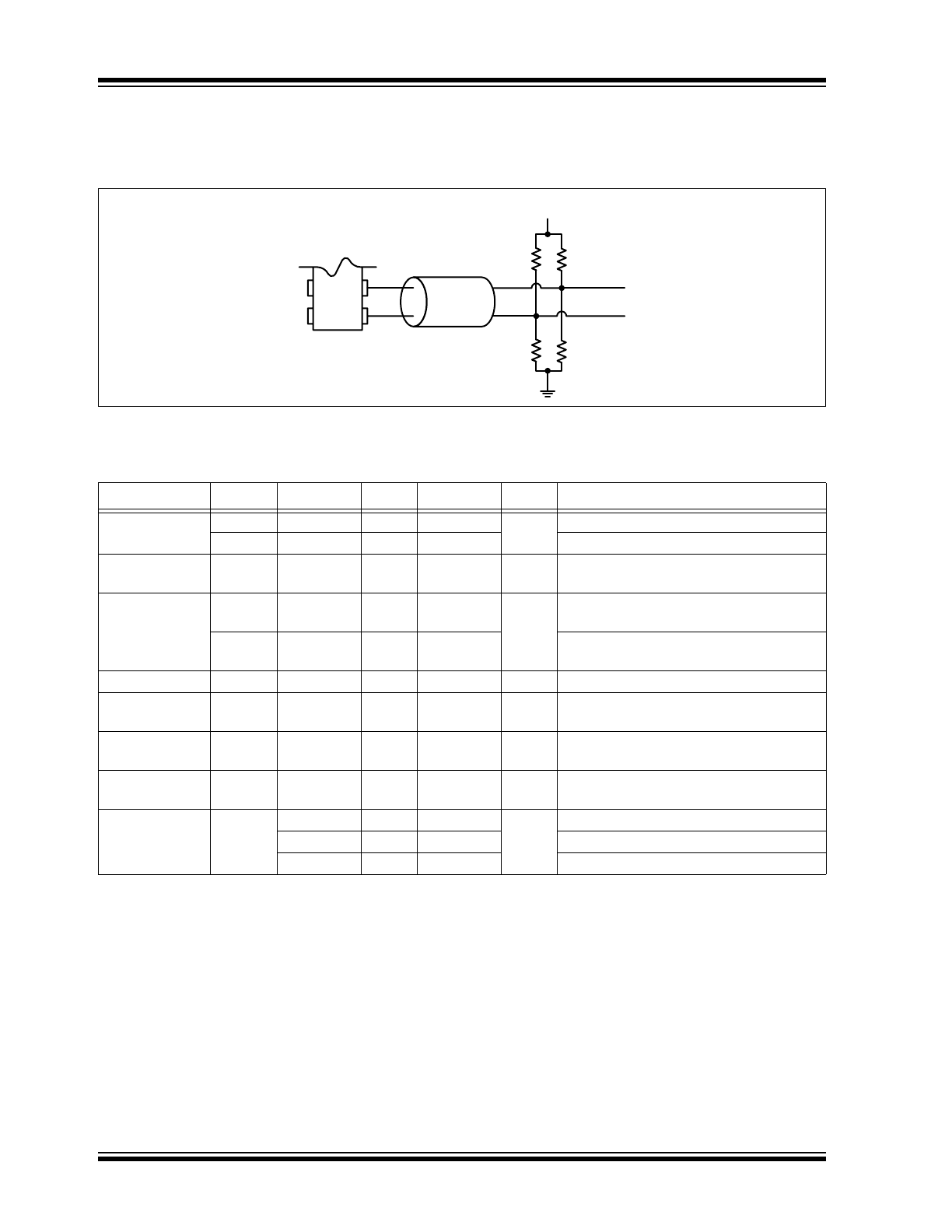
LVDS
FIGURE 4-2:
Typical LVDS Termination Scheme.
If the 100Ω clamping resistor does not exist inside the receiving device, it should be added externally on the PCB and
placed as close as possible to the receiver.
Note 1:
See the
Output Waveform
section for more information.
2:
The addition of I
DDCORE
and I
DDIO
provides the total current consumption of the device.
TABLE 4-2:
LVDS OUTPUTS
Parameter
Symbol
Min.
Typ.
Max.
Units
Condition
Output Offset
Voltage
V
OS
1.125
—
1.4
V
R = 100Ω Differential
Delta Offset
Voltage
∆V
OS
—
—
50
mV
—
Peak-to-Peak
Output Swing
V
PP
—
350
—
mV
Single-Ended
Output
Transition Time
(
Note 1
)
t
R
—
200
—
ps
Rise Time, 20% to 80%, R
L
= 50Ω,
C
L
= 2 pF
t
F
—
200
—
Fall Time, 20% to 80%, R
L
= 50Ω,
C
L
= 2 pF
Frequency
f
0
2.3
—
460
MHz
Single Frequency
Output Duty
Cycle
SYM
48
—
52
%
Differential
IO Supply
Current (
Note 2
)
I
DDIO
—
9
12
mA
Per Output at 125 MHz.
Period Jitter
J
PER
—
2.5
—
ps
RMS
—
Integrated
Phase Noise
J
PH
—
0.28
—
ps
RMS
200 kHz to 20 MHz @ 156.25 MHz
—
0.4
—
100 kHz to 20 MHz @ 156.25 MHz
—
1.7
2.0
12 kHz to 20 MHz @156.25 MHz
100 Ω
100 Ω
Load (receiver IC)
DSC400
DS20005612A-page 8
2016 Microchip Technology Inc.
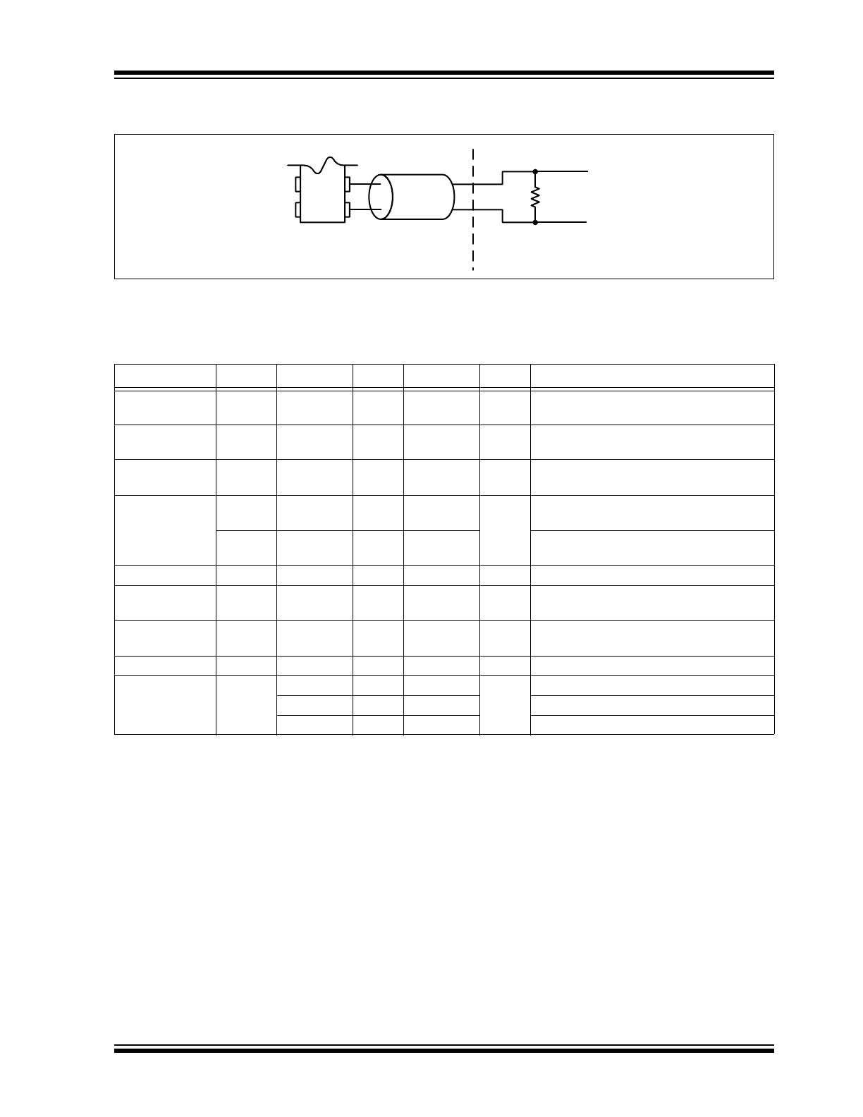
4.3
HCSL
FIGURE 4-3:
Typical HCSL Termination Scheme.
R
S
is a series resistor implemented to match the trace impedance. Depending on the board layout, the value may range
from 0Ω to 30Ω.
Note 1:
See the
Output Waveform
section for more information.
2:
The addition of I
DDCORE
and I
DDIO
provides the total current consumption of the device.
TABLE 4-3:
HCSL OUTPUTS
Parameter
Symbol
Min.
Typ.
Max.
Units
Condition
Output Logic
Levels
V
OH
0.725
—
—
V
Output Logic High, R
L
= 50Ω
V
OL
—
—
0.1
Output Logic Low, R
L
= 50Ω
Peak-to-Peak
Output Swing
—
—
750
—
mV
Single-Ended
Output
Transition Time
(
Note 1
)
t
R
200
—
400
ps
Rise Time, 20% to 80%, R
L
= 50Ω,
C
L
= 2 pF
t
F
200
—
400
Fall Time, 20% to 80%, R
L
= 50Ω,
C
L
= 2 pF
Frequency
f
0
2.3
—
460
MHz
Single Frequency
Output Duty
Cycle
SYM
48
—
52
%
Differential
IO Supply
Current (
Note 2
)
I
DDIO
—
20
22
mA
Per Output at 125 MHz.
Period Jitter
J
PER
—
2.5
—
ps
RMS
—
Integrated
Phase Noise
J
PH
—
0.25
—
ps
RMS
200 kHz to 20 MHz @ 156.25 MHz
—
0.37
—
100 kHz to 20 MHz @ 156.25 MHz
—
1.7
2.0
12 kHz to 20 MHz @156.25 MHz
100 Ω
50 Ω
50 Ω
R
S
R
S
2016 Microchip Technology Inc.
DS20005612A-page 9
DSC400
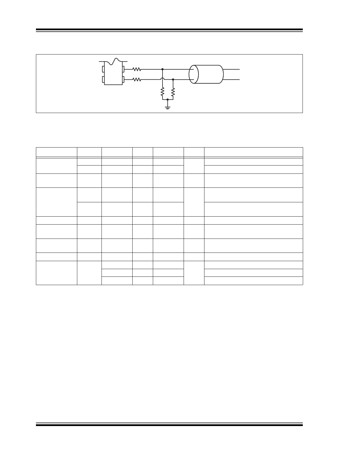
4.4
LVCMOS
FIGURE 4-4:
Typical LVCMOS Termination Scheme.
R
S
is a series resistor implemented to match the trace impedance to that of the clock output. Depending on the board
layout, the value may range from 0Ω to 27Ω.
Note 1:
See the
Output Waveform
section for more information.
2:
The addition of I
DDCORE
and I
DDIO
provides the total current consumption of the device.
TABLE 4-4:
LVCMOS OUTPUTS
Parameter
Symbol
Min.
Typ.
Max.
Units
Condition
Output Logic
Levels
V
OH
0.9 x V
DD
—
—
V
Output Logic High, I = ±6 mA
V
OL
—
—
0.1 x V
DD
Output Logic Low, I = ±6 mA
Output
Transition Time
(
Note 1
)
t
R
—
1.1
2.0
ns
Rise Time, 20% to 80%, C
L
= 15 pF
t
F
—
1.3
2.0
Fall Time, 20% to 80%, C
L
= 15 pF
Frequency
f
0
2.3
—
170
MHz
All Temperature Ranges, Except
Automotive
—
—
100
Automotive Temperature Range
Output Duty
Cycle
SYM
44
—
55
%
—
IO Supply
Current (
Note 2
)
I
DDIO
—
11
14
mA
Per Output at 125 MHz, C
L
= 15 pF
Period Jitter
J
PER
—
3
—
ps
RMS
CLK(0:3) = 125 MHz
Integrated
Phase Noise
J
PH
—
0.3
—
ps
RMS
200 kHz to 20 MHz @ 125 MHz
—
0.38
—
100 kHz to 20 MHz @ 125 MHz
—
1.7
2.0
12 kHz to 20 MHz @125 MHz
50 Ω
R
S
DSC400
DS20005612A-page 10
2016 Microchip Technology Inc.
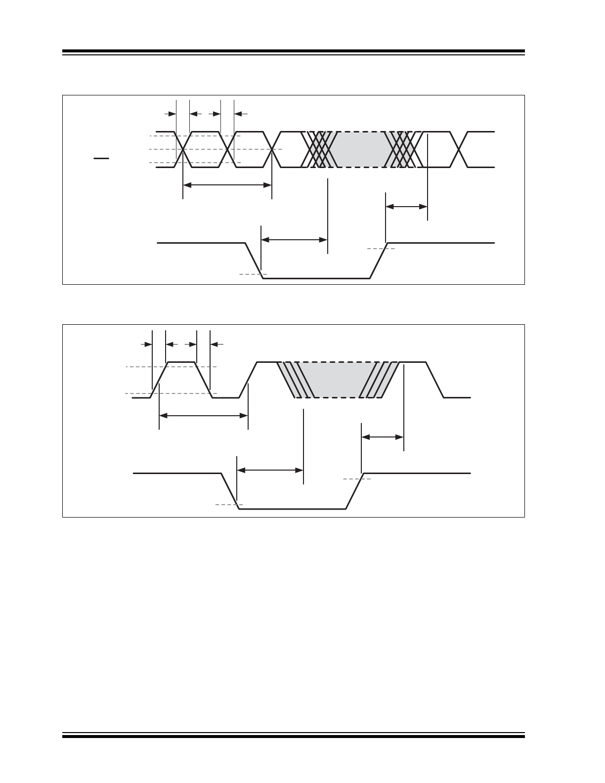
5.0
OUTPUT WAVEFORM
FIGURE 5-1:
Differential Output (LVDS, LVPECL, HCSL).
FIGURE 5-2:
LVCMOS Output.
OE
t
R
t
F
1/f
0
t
DA
t
EN
Clk
Clk
V
IL
V
IH
50%
20%
80%
OE
t
R
t
F
1/f
0
t
DA
t
EN
Clk
V
IL
V
IH
V
OL
V
OH