
2017 Microchip Technology Inc.
DS20005758A-page 1
MIC841/2
Features
• 1.5V to 5.5V Operating Range
• 1.5 μA Typical Supply Current
• ±1.25% Voltage Threshold Accuracy
• 10 nA Maximum Input Leakage Current Over
Temperature
• 10 μs Propagation Delay
• Externally Adjustable Hysteresis (MIC841)
• Internal 20 mV Hysteresis (MIC842)
• Output Options:
- Push-Pull, Active-High
- Push-Pull, Active-Low
- Open-Drain, Active-Low
• Open-Drain Output can be Pulled to 6V
Regardless of V
DD
• Immune to Brief Input Transients
• Teeny 5-Pin SC-70 Package
• 6-Pin 1.6 mm x 1.6 mm TDFN (MIC841)
• 4-Pin 1.2 mm x 1.6 mm TDFN (MIC842)
Applications
• Smartphones
• PDAs
• Precision Battery Monitoring
• Battery Chargers
General Description
The MIC841 and MIC842 are micro-power,
precision-voltage comparators with an on-chip voltage
reference.
Both devices are intended for voltage monitoring
applications. External resistors are used to set the
voltage monitor threshold. When the threshold is
crossed, the outputs switch polarity.
The MIC842 incorporates a voltage reference and
comparator with fixed internal hysteresis; two external
resistors are used to set the switching threshold
voltage. The MIC841 provides a similar function with
user adjustable hysteresis; this part requires three
external resistors to set the upper and lower thresholds
(the difference between the threshold voltages being
the hysteresis voltage).
Both the MIC841 and MIC842 are available with
push-pull or open-drain output stage. The push-pull
output stage is configured either active-high or
active-low; the open-drain output stage is only
configured active-low.
Supply current is extremely low (1.5 μA, typical),
making it ideal for portable applications.
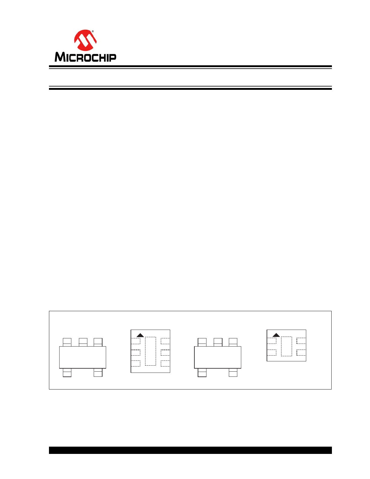
The MIC841/2 is supplied in the Teeny 5-pin SC-70,
6-pin 1.6 mm × 1.6 mm Thin DFN (MIC841), and 4-pin
1.2 mm × 1.6 mm Thin DFN (MIC842) packages.
Package Types
MIC841
SC-70-5 (C5)
LTH GND HTH
OUT
VDD
Yxx
3
2
1
4
5
MIC841
6-Pin TDFN (MT)
LTH
GND
HTH
OUT
NC
VDD
1
2
3
6
5
4
EP
MIC842
SC-70-5 (C5)
NC GND INP
OUT
VDD
Yxx
3
2
1
4
5
MIC842
4-Pin TDFN (MT)
OUT
GND
VDD
INP
1
2
3
4
EP
Comparator with 1.25% Reference and Adjustable Hysteresis
MIC841/2
DS20005758A-page 2
2017 Microchip Technology Inc.
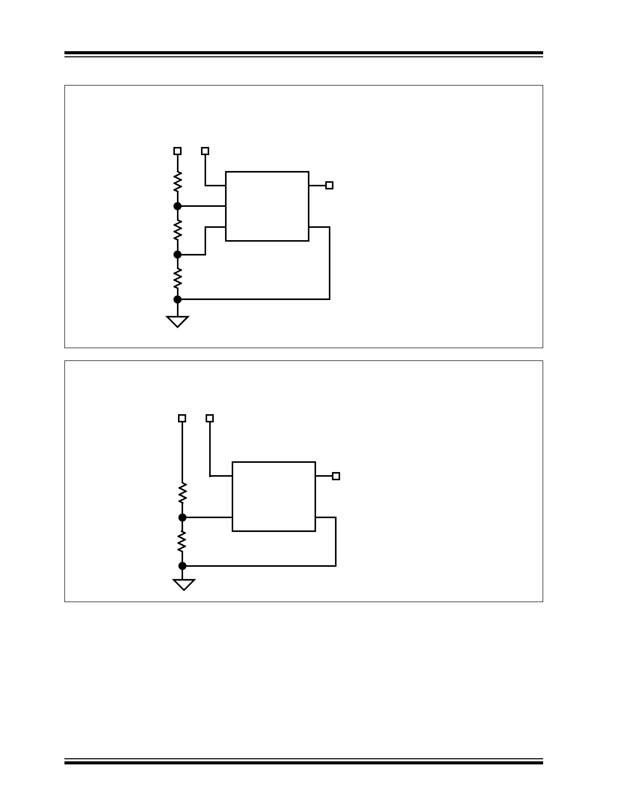
Typical Application Circuits
MIC841
Threshold Detection with Adjustable Hysteresis
HTH
OUT
VDD
LTH
GND
MIC841
V
IN
R1
R2
R3
V
OUT
V
DD
V
LTH
> V
HTH
V
REF
= 1.24V
99
DD
9
MIC842
Threshold Detection with Internal Fixed Hysteresis
INP
OUT
VDD
GND
V
IN
R1
V
OUT
V
DD
V
REF
= 1.24V
99
DD
9
MIC842
R2
2017 Microchip Technology Inc.
DS20005758A-page 3
MIC841/2
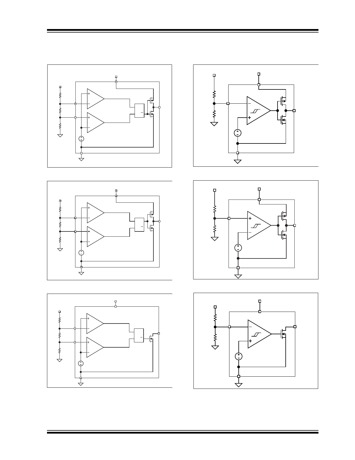
1.0
FUNCTIONAL BLOCK DIAGRAMS
Note:
Block diagrams show SC-70 package pin numbers.
FIGURE 1-1:
MIC841H Block Diagram
FIGURE 1-2:
MIC841L Block Diagram
FIGURE 1-3:
MIC841N Block Diagram
FIGURE 1-4:
MIC842H Block Diagram
FIGURE 1-5:
MIC842L Block Diagram
FIGURE 1-6:
MIC842N Block Diagram
GND
V
DD
OUT
1.24V
BANDGAP
REFERENCE
LOW-VOLTAGE
DETECT
HIGH-VOLTAGE
DETECT
R
S
Q
Q
LTH
HTH
V
LTH
V
HTH
MIC841H
V
IN
3
1
2
4
5
V
DD
GND
V
DD
OUT
1.24V
BANDGAP
REFERENCE
LOW-VOLTAGE
DETECT
HIGH-VOLTAGE
DETECT
R
S
Q
Q
LTH
HTH
V
LTH
V
HTH
MIC841L
V
DD
V
IN
3
1
2
4
5
GND
V
DD
OUT
1.24V
BANDGAP
REFERENCE
LOW-VOLTAGE
DETECT
HIGH-VOLTAGE
DETECT
R
S
Q
Q
LTH
HTH
V
LTH
V
HTH
MIC841N
V
IN
3
1
2
4
5
V
DD
GND
V
IN
1.24V
BANDGAP
REFERENCE
HIGH-VOLTAGE
DETECT
INP
V
TH
MIC842H
2
1
5
V
DD
OUT
4
V
DD
GND
V
IN
1.24V
BANDGAP
REFERENCE
HIGH-VOLTAGE
DETECT
INP
V
TH
MIC842L
2
1
5
V
DD
OUT
4
V
DD
GND
V
IN
OUT
1.24V
BANDGAP
REFERENCE
HIGH-VOLTAGE
DETECT
INP
V
TH
MIC842N
4
2
1
5
V
DD
V
DD

MIC841/2
DS20005758A-page 4
2017 Microchip Technology Inc.
2.0
ELECTRICAL CHARACTERISTICS
Absolute Maximum Ratings †
Supply Voltage (V
DD
) ................................................................................................................................... –0.3V to +7V
Input Voltage (V
INP
, V
LTH
,V
HTH
) ..................................................................................................................................+7V
Output Current (I
OUT
) ............................................................................................................................................±20 mA
ESD Rating
(
1
)
.............................................................................................................................................................1 kV
Operating Ratings ‡
Supply Voltage (V
DD
) ................................................................................................................................ +1.5V to +5.5V
Input Voltage (V
INP
, V
LTH
,V
HTH
) ........................................................................................................................ 0V to +6V
V
OUT
(‘H’ and ‘L’ versions) ......................................................................................................................................... V
DD
V
OUT
(‘N’ version)........................................................................................................................................................+6V
†
Notice: Stresses above those listed under “Absolute Maximum Ratings” may cause permanent damage to the device.
This is a stress rating only and functional operation of the device at those or any other conditions above those indicated
in the operational sections of this specification is not intended. Exposure to maximum rating conditions for extended
periods may affect device reliability.
‡ Notice:
The device is not guaranteed to function outside its operating ratings.
Note 1:
Devices are ESD sensitive. Handling precautions are recommended. Human body model, 1.5 kΩ in series
with 100 pF.
2017 Microchip Technology Inc.
DS20005758A-page 5
MIC841/2
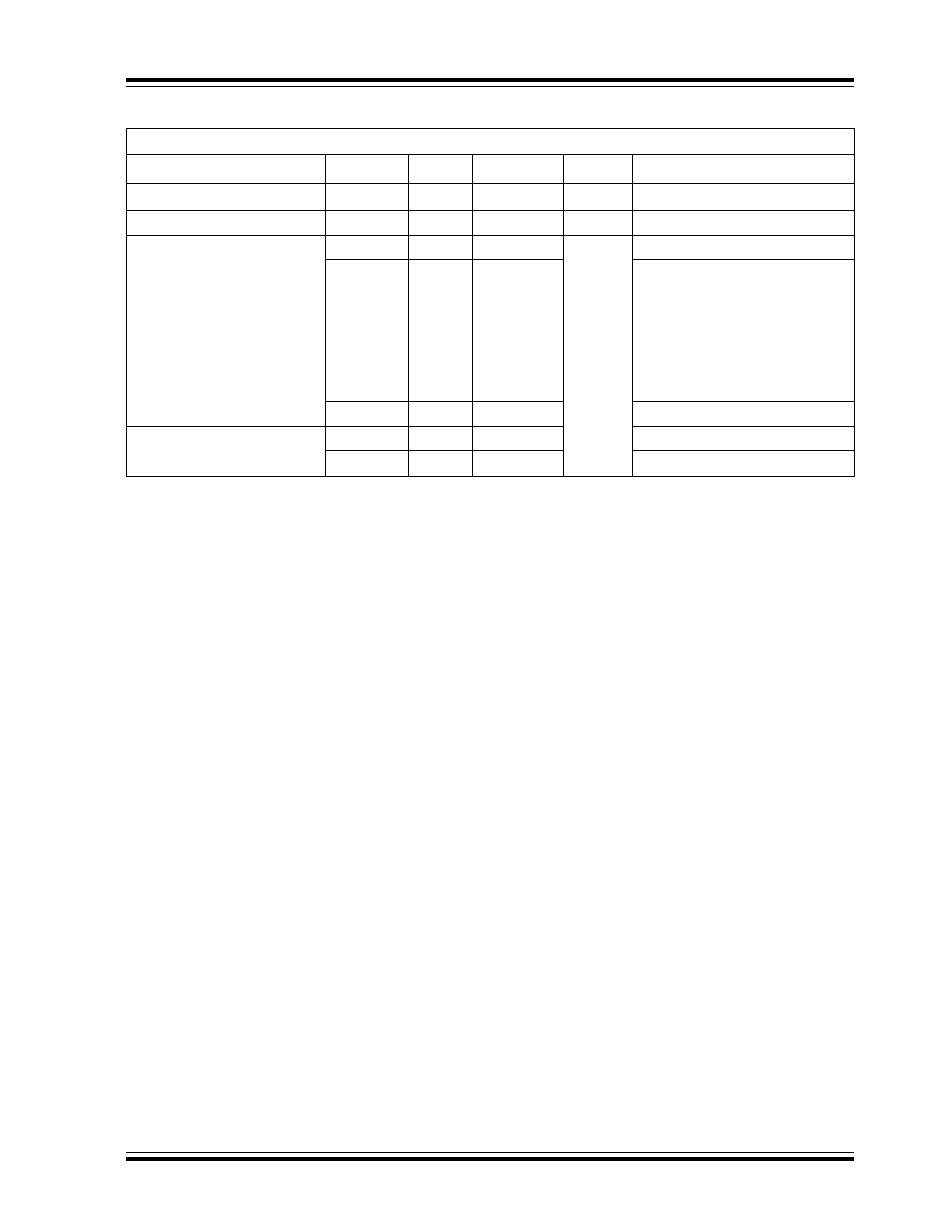
TABLE 2-1:
ELECTRICAL CHARACTERISTICS
Electrical Characteristics:
1.5V ≤ V
DD
≤ 5.5V; T
A
= 25°C. –40°C ≤ T
A
≤ +85°C, unless noted. (
Note 1
)
.
Parameters
Min.
Typ.
Max.
Units
Conditions
Supply Current (I
DD
)
—
1.5
3
µA
Output not asserted
Input Leakage Current (I
INP
)
—
0.005
10
nA
—
Reference Voltage (V
REF
)
1.225
1.240
1.256
V
0°C ≤ T
A
≤ 85°C
1.219
1.240
1.261
–40°C ≤ T
A
≤ 85°C
Hysteresis Voltage (V
HYST
)
(
Note 2
)
8
20
35
mV
MIC842 only
Propagation Delay (t
D
)
—
12
50
µs
V
INP
= 1.352V to 1.128V
—
8
50
V
INP
= 1.143V to 1.367V
Output Voltage-Low (V
OUT
)
(
Note 3
)
—
0.05
0.3
V
I
SINK
= 1.6 mA, V
DD
≥ 1.6V
—
0.005
0.4
I
SINK
= 100 µA, V
DD
≥ 1.2V
Output Voltage-High (V
OUT
)
(
Note 3
)
—
0.99V
DD
—
I
SOURCE
= 500 µA, V
DD
≥ 1.6V
—
0.99V
DD
—
I
SOURCE
= 50 µA, V
DD
≥ 1.2V
Note 1:
Specification for packaged product only.
2:
V
HTH
= V
REF
+ V
HYST
.
3:
V
DD
operating range is 1.5V to 5.5V. Output is guaranteed to be de-asserted down to V
DD
= 1.2V.
MIC841/2
DS20005758A-page 6
2017 Microchip Technology Inc.
TEMPERATURE SPECIFICATIONS
Parameters
Sym.
Min.
Typ.
Max.
Units
Conditions
Temperature Ranges
Maximum Junction Temperature
T
J
—
—
+150
°C
Note 1
Storage Temperature Range
T
S
–65
—
+150
°C
—
Ambient Temperature Range
T
A
–40
—
+85
°C
—
Lead Temperature
—
—
—
+260
°C
Soldering, 10s
Package Thermal Resistances
SC-70-5
JA
—
256.5
—
°C/W
—
6-Pin 1.6 mm x 1.6 mm TDFN
JA
—
92
—
°C/W
—
4-Pin 1.2 mm x 1.6 mm TDFN
JA
—
173
—
°C/W
—
Note 1:
The maximum allowable power dissipation is a function of ambient temperature, the maximum allowable
junction temperature and the thermal resistance from junction to air (i.e., T
A
, T
J
,
JA
). Exceeding the
maximum allowable power dissipation will cause the device operating junction temperature to exceed the
maximum +150°C rating. Sustained junction temperatures above +150°C can impact the device reliability.
2017 Microchip Technology Inc.
DS20005758A-page 7
MIC841/2
3.0
PIN DESCRIPTIONS
The descriptions of the pins are listed in
Table 3-1
and
Table 3-2
.
TABLE 3-1:
MIC841 PIN FUNCTION TABLE
Pin Number
SC-70
Pin Number
TDFN
Symbol
Description
1
3
HTH
High Threshold Input. HTH and LTH monitor external
voltages.
2
2
GND
Ground.
3
1
LTH
Low Threshold Input. LTH and HTH monitor external voltages.
4
6
OUT
(“H” Version) Active-Low Push-Pull Output. OUT asserts low
when V
LTH
< V
REF
. OUT remains low until V
HTH
> V
REF
.
OUT
(“L” Version) Active-High Push-Pull Output. OUT asserts high
when V
LTH
< V
REF
. OUT remains high until V
HTH
> V
REF
.
OUT
(“N” Version) Active-Low, Open-Drain Output. OUT asserts
low when V
LTH
< V
REF
. OUT remains low until V
HTH
> V
REF
.
5
4
VDD
Power Supply Input.
—
5
NC
No Connect. Not internally connected.
—
EP
ePAD
Heatsink Pad. Connect to GND for best thermal performance.
TABLE 3-2:
MIC842 PIN FUNCTION TABLE
Pin Number
SC-70
Pin Number
TDFN
Symbol
Description
1
3
INP
Threshold Input. INP monitors an external voltage.
2
2
GND
Ground.
3
—
NC
No Connect. Not internally connected.
4
1
OUT
(“H” Version) Active-Low, Push-Pull Output. OUT asserts low
when V
INP
< V
REF
. OUT remains low until V
INP
> (V
REF
+
V
HYST
).
OUT
(“L” Version) Active-High, Push-Pull Output. OUT asserts high
when V
INP
< V
REF
. OUT remains high until V
INP
> (V
REF
+
V
HYST
).
OUT
(“N” Version) Active-Low, Open-Drain Output. OUT asserts
low when V
INP
< V
REF
. OUT remains low until V
INP
> (V
REF
+
V
HYST
).
5
4
VDD
Power Supply Input.
—
EP
ePAD
Heatsink Pad. Connect to GND for best thermal performance.
MIC841/2
DS20005758A-page 8
2017 Microchip Technology Inc.
4.0
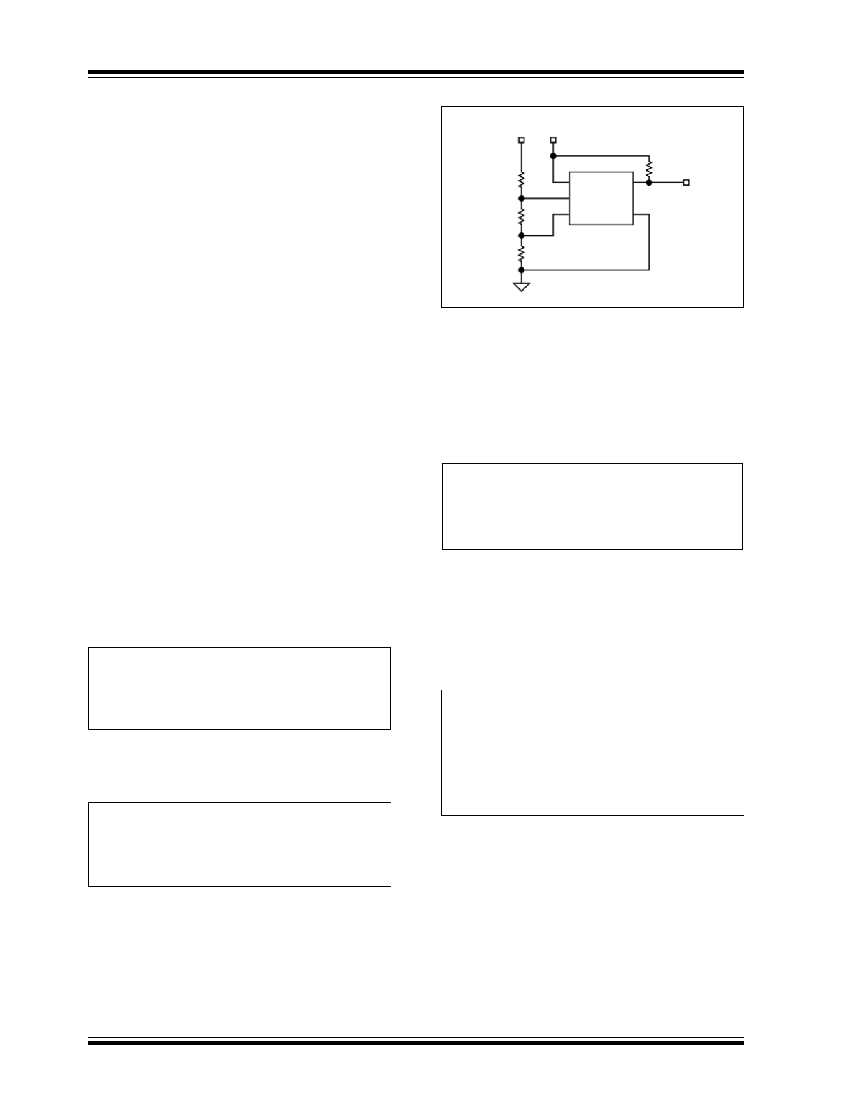
APPLICATION INFORMATION
4.1
Output
The MIC841N and MIC842N outputs are an open-drain
MOSFET, so most applications will require a pull-up
resistor. The value of the resistor should not be too
large or leakage effects may dominate. 470 kΩ is the
maximum recommended value. Note that the output of
the “N” version may be pulled up as high as 6V
regardless of the IC’s supply voltage. The “H” and “L”
versions of the MIC841 and MIC842 have a push-pull
output stage with a diode clamped to V
DD
. Thus, the
maximum output voltage of the “H” and “L” versions is
V
DD
(see
Table 2-1
).
When working with large resistors on the input to the
devices, a small amount of leakage current can cause
voltage offsets that degrade system accuracy. The
maximum recommended total resistance from V
IN
to
ground is 3 MΩ. The accuracy of the resistors can be
chosen based upon the accuracy required by the
system. The inputs may be subjected to voltages as
high as 6V steady-state without adverse effects of any
kind regardless of the IC’s supply voltage. This applies
even if the supply voltage is zero. This permits the
situation in which the IC’s supply is turned off, but
voltage is still present on the inputs (see
Table 2-1
).
4.2
Programming the MIC841
Thresholds
The low-voltage threshold is calculated using
Equation 4-1
.
EQUATION 4-1:
The high-voltage threshold is calculated using
Equation 4-2
.
EQUATION 4-2:
In order to provide the additional criteria needed to
solve for the resistor values, the resistors can be
selected such that they have a given total value, that is,
R1 + R2 + R3 = R
TOTAL
. A value such as 1 MΩ for
R
TOTAL
is a reasonable value because it draws
minimum current but has no significant effect on
accuracy.
FIGURE 4-1:
MIC841 Example Circuit
Once the desired trip points are determined, set the
V
IN(HI)
threshold first.
For example, use a total of 1 MΩ = R1 + R2 + R3. For
a typical single-cell lithium ion battery, 3.6V is a good
“high threshold” because at 3.6V the battery is
moderately charged. Solving for R3:
EQUATION 4-3:
Once R3 is determined, the equation for V
IN(LO)
can be
used to determine R2. A single lithium-ion cell, for
example, should not be discharged below 2.5V. Many
applications limit the drain to 3.1V.
Using 3.1V for the V
IN(LO)
threshold allows the
calculation of the two remaining resistor values.
EQUATION 4-4:
The accuracy of the resistors can be chosen based
upon the accuracy required by the system.
V
IN LO
V
REF
R1
R2
R3
+
+
R2
R3
+
---------------------------------
=
Where:
V
REF
1.240V
V
IN HI
V
REF
R1
R2
R3
+
+
R3
---------------------------------
=
Where:
V
REF
1.240V
V
IN
R1
604k 1%
R2
56k 1%
R3
340k 1%
V
DD
VDD
LTH
HTH
OUT
GND
470k
V
OUT
MIC841N
V
IN HI
3.6V
1.24V
1M
R3
-------------
=
=
Solve:
R3
344 kΩ
V
IN LO
3.1V
1.24V
1M
R2
344k
+
------------------------------
=
=
Solve:
R2
56 kΩ
R1
1 MΩ - R2 - R3
R1
600 kΩ
2017 Microchip Technology Inc.
DS20005758A-page 9
MIC841/2
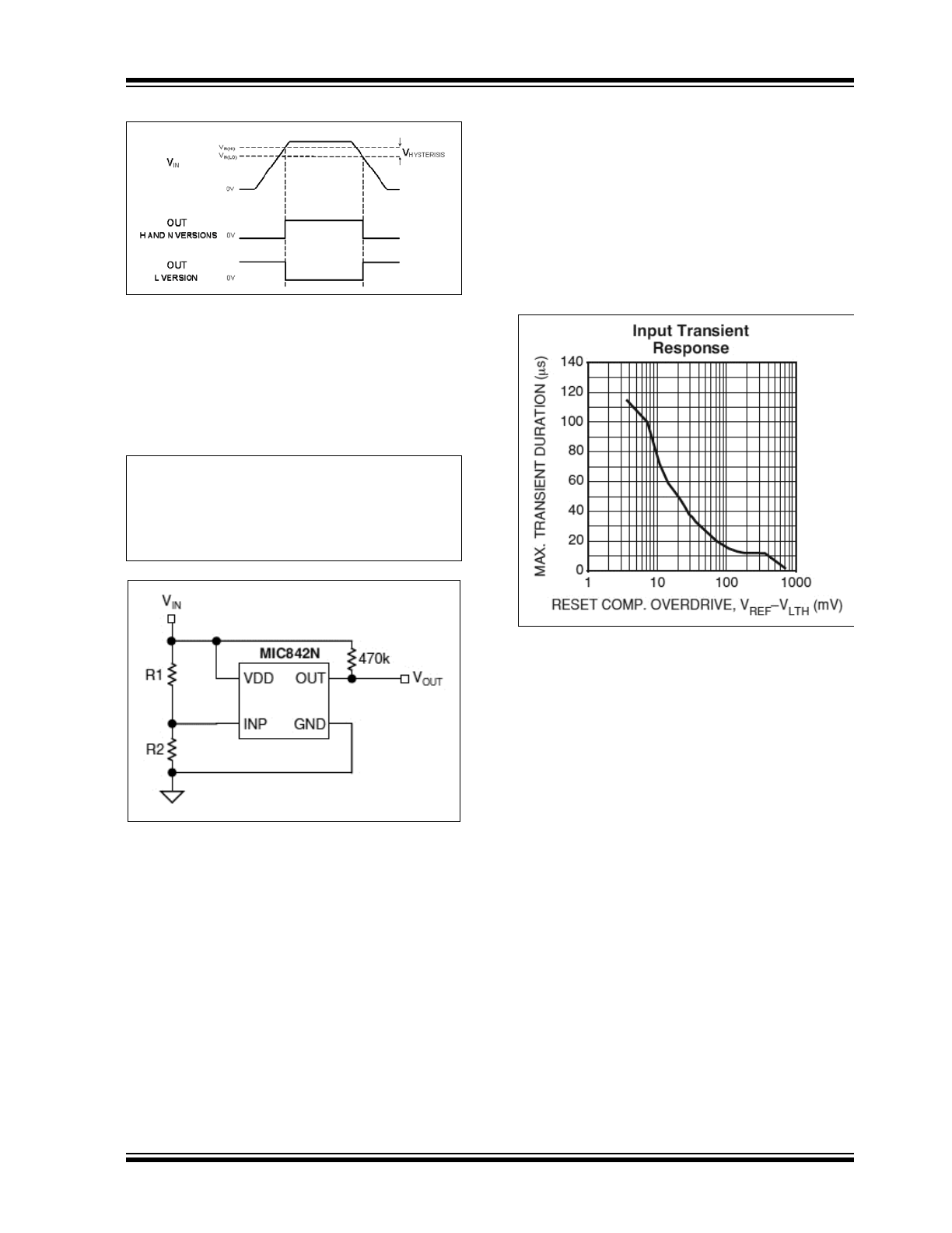
FIGURE 4-2:
Output Response and
Hysteresis
4.3
Programming the MIC842
Thresholds
The voltage threshold is calculated using
Equation 4-5
.
EQUATION 4-5:
FIGURE 4-3:
MIC842 Example Circuit
In order to provide the additional criteria needed to
solve for the resistor values, the resistors can be
selected such that they have a given total value, that is,
R1 + R2 = R
TOTAL
. A value such as 1 MΩ for R
TOTAL
is
a reasonable value because it draws minimum current,
but has no significant effect on accuracy.
4.4
Input Transients
The MIC841/2 is inherently immune to very short
negative-going “glitches.” Very brief transients may
exceed the V
IN(LO)
threshold without tripping the
output.
As shown in
Figure 4-4
, the narrower the transient, the
deeper the threshold overdrive that will be ignored by
the MIC841/2. The graph represents the typical
allowable transient duration for a given amount of
threshold overdrive that will not generate an output.
FIGURE 4-4:
Input Transient Response
V
IN LO
V
REF
R1
R2
+
R2
--------------------
=
Where:
V
REF
1.240V
MIC841/2
DS20005758A-page 10
2017 Microchip Technology Inc.
5.0
PACKAGING INFORMATION
5.1
Package Marking Information
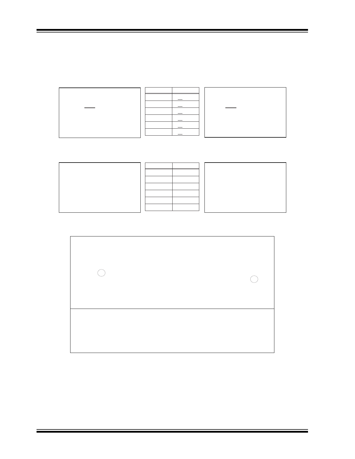
5-Pin SC-70*
Example
XXX
NNN
4-Pin TDFN*
Example
XX
B14
408
6-Pin TDFN*
Ÿ
BL
Ÿ
Device
Marking
MIC841H B13
MIC841L B14
MIC841N B15
MIC842H B16
MIC842L B17
MIC842N B18
Device
Marking
MIC841H BH
MIC841L BL
MIC841N BN
MIC842H HB
MIC842L HL
MIC842N HN
Legend:
XX...X
Product code or customer-specific information
Y
Year code (last digit of calendar year)
YY
Year code (last 2 digits of calendar year)
WW
Week code (week of January 1 is week ‘01’)
NNN
Alphanumeric traceability code
Pb-free JEDEC
®
designator for Matte Tin (Sn)
*
This package is Pb-free. The Pb-free JEDEC designator ( )
can be found on the outer packaging for this package.
●, ▲, ▼ Pin one index is identified by a dot, delta up, or delta down (triangle
mark).
Note
:
In the event the full Microchip part number cannot be marked on one line, it will
be carried over to the next line, thus limiting the number of available
characters for customer-specific information. Package may or may not include
the corporate logo.
Underbar (_) and/or Overbar (⎯) symbol may not be to scale.
3
e
3
e