
R&E International
A Subsidiary of Microchip Technology Inc.
RE46C152
CMOS Ionization Smoke Detector ASIC with Interconnect, Timer Mode and Tone Select
Product Specification
© 2009 Microchip Technology Inc.
DS22175A-page 1
General Description
The RE46C152 is a low power CMOS ionization type
smoke detector IC. With few external components this
circuit will provide all the required features for an
ionization type smoke detector.
An internal oscillator strobes power to the smoke
detection circuitry for 10.5mS every 1.66 seconds to
keep standby current to a minimum. A check for a low
battery condition is performed every 40 seconds when
in standby. The Tone input allows for selection of a
temporal pattern or a 2/3 duty cycle continuous tone.
The temporal horn pattern supports the NFPA 72
emergency evacuation signal.
An interconnect pin allows multiple detectors to be
connected such that when one units alarms all units will
sound.
An internal 8 minute timer allows for a separate button
to be used for reduced sensitivity mode. Single button
operation for test and timer mode is also possible.
Although this device was designed for smoke detection
utilizing an ionization chamber it could be used in a
variety of security applications.
Utilizing low power CMOS technology the RE46C152
was designed for use in smoke detectors that comply
with Underwriters Laboratory Specification UL217 and
UL268.
Features
• >1500V ESD Protection (HBM) on all Pins
• Guard Outputs for Ion Detector Input
• +/-0.75pA Detect Input Current
• Internal Reverse Battery Protection
• Low Quiescent Current Consumption (<6.5uA)
• 16L
PDIP
• Internal Low Battery Detection
• Power Up Low Battery Test
• Interconnect up to 40 Detectors
• Pin selectable horn patterns
• 8 Minute Timer for Sensitivity Control
• Available in RoHS Compliant Pb Free Packaging.
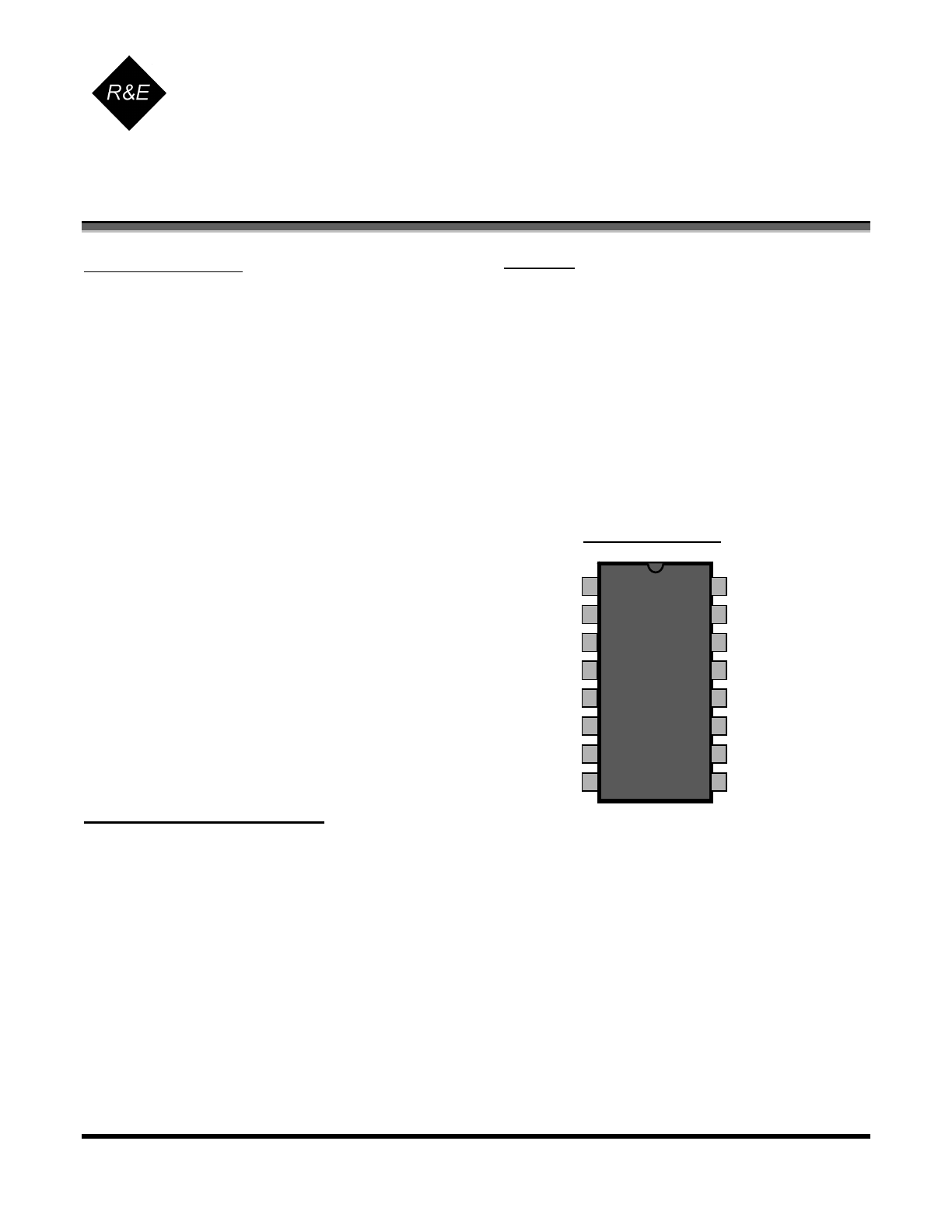
Pin Configuration
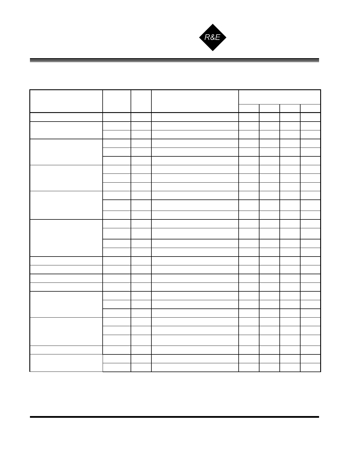
ABSOLUTE MAXIMUM RATINGS
PARAMETER SYMBOL
VALUE
UNITS
Supply Voltage
V
DD
15 V
Input Voltage Range Except FEED, IO
V
in
-.3 to V
dd
+.3 V
FEED Input Voltage Range
V
infd
-10 to +22
V
IO Input Voltage Range
V
io1
-.3 to 17
V
Reverse Battery Time
T
RB
5 S
Input Current except FEED
I
in
10
MA
Operating Temperature
T
A
-10 to 60
°C
Storage Temperature
T
STG
-55 to 125
°C
Maximum Junction Temperature
T
J
150
°C
16
GUARD2
1
TSTART
2
DETECT
IO
15
3
GUARD1
TONE
14
TSTROBE
4
VSEN
13
Stresses beyond those listed under Absolute Maximum Ratings may cause permanent damage to the device. These are
stress ratings only and operation at these conditions for extended periods may affect device reliability.
This product utilizes CMOS technology with static protection; however proper ESD prevention procedures should be used
when handling this product. Damage can occur when exposed to extremely high static electrical charge.
5
OSCAP
12
LED
VDD
RBIAS
FEED
6
HS
11
7
HB
10
VSS
8
9
RE46C152
CMOS Ionization Smoke Detector ASIC with Interconnect, R&E International
Timer Mode and Tone Select
A Subsidiary of Microchip Technology
Inc.
Product Specification
© 2009 Microchip Technology Inc.
DS22175A-page 2
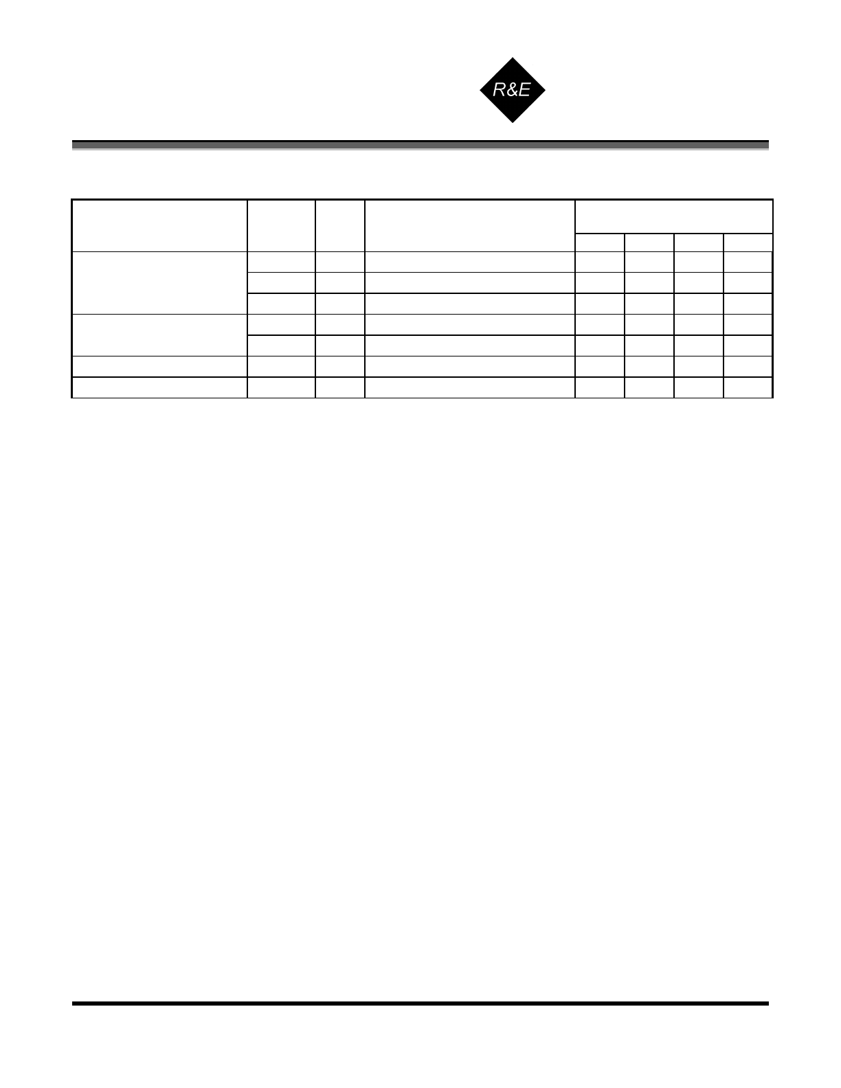
DC Electrical Characteristics at TA = 25°C, VDD=9V, OSCAP=.1uF, RBIAS=8.2MΩ, VSS=0V (unless
otherwise noted)
Limits
Parameter Symbol
Test
Pin Test
Conditions Min Typ Max Units
Supply Voltage
V
DD
6
Operating
6 12
V
I
DD1
6
RBIAS=8.2MΩ, OSCAP=.1uF
5
6.5
uA
Supply Current
I
DD2
6
RBIAS=8.2MΩ, OSCAP=.1uF;Vdd=12V
9
uA
V
IH1
3,8
6.2 4.5
V
V
IH2
2
No Local Alarm, IO as an Input
3
V
Input Voltage High
V
IH3
1
4.5 V
V
IL1
3,8
4.5 2.7 V
V
IL2
2
No Local Alarm, IO as an Input
1
V
Input Voltage Low
V
IL3
1
2.5
V
IL
DET1
15
VDD=9V, DETECT=VSS, 0-40% RH
-0.75
pA
IL
DET2
15
VDD=9V, DETECT=VSS, 85% RH
Note 1
-1.50
pA
Input Leakage Low
IL
FD
8
FEED=-10V
-50
uA
IH
DET1
15
VDD=9V, DETECT=VDD, 0-40% RH
0.75
pA
IH
DET2
15
VDD=9V, DETECT=VDD, 85% RH
Note 1
1.50
pA
IH
FD
8
FEED=22V
50
uA
Input Leakage High
I
IOL2
2
No Alarm, Vio=17V
150
uA
Output Off Leakage High
I
IOHZ
4,5
Outputs Off
1
uA
Input Pull Up Current
I
PU1
3
TONE=VSS, RBIAS=8.2MΩ
-50 -800
nA
Input Pull Down Current
I
PD1
1
TSTART=9V
20 50 80 uA
Output High Voltage
V
OH1
10,11
IOH=-16mA, VDD=7.2V
6.3 V
V
OL1
10,11
IOL=16mA, VDD=7.2V
.9
V
V
OL2
4
IOL=500ua
.5
V
Output Low Voltage
V
OL3
5
IOL=10mA, VDD=7.2V
1
V
I
IOL1
2
No Alarm, Vio=Vdd-2V
25 60
uA
I
IOH1
2
Alarm, Vio=Vdd-2V or Vio=0V
-4 -16
mA
Output Current
I
IODMP
2
At Conclusion of Local Alarm or Test,
Vio=1V
5 mA
Low Battery Voltage
V
LB
6
T
A
=-10 to 60ºC, Note 3
7.2 7.5 7.8 V
V
SET1
13
48.5 50 51.5
%V
DD
Internal Sensitivity Set Voltage
V
SET2
RE46C152
CMOS Ionization Smoke Detector ASIC with Interconnect, R&E International
Timer Mode and Tone Select
A Subsidiary of Microchip Technology
Inc.
Product Specification
© 2009 Microchip Technology Inc.
DS22175A-page 3
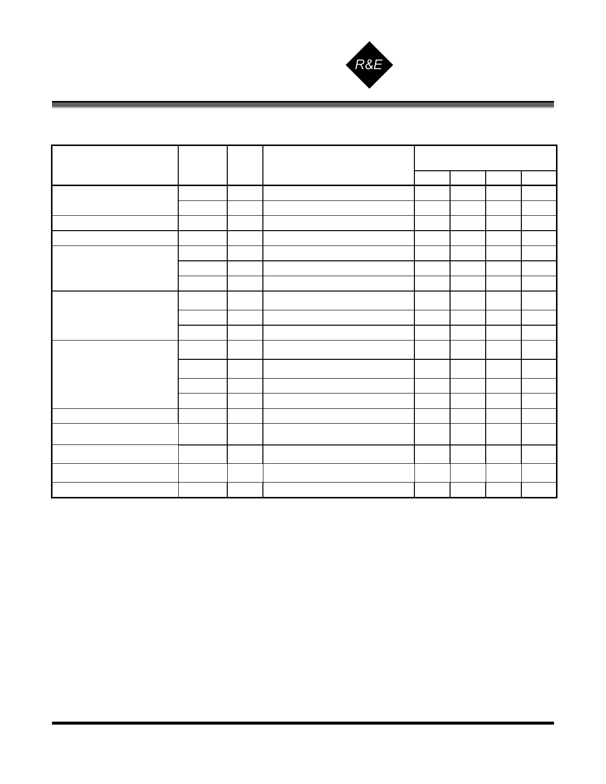
DC Electrical Characteristics – Continued
Limits
Parameter Symbol
Test
Pin Test
Conditions Min Typ Max Units
VG
OS1
14,15
Guard Amplifier
-50 50
mV
VG
OS2
15,16
Guard Amplifier
-50 50
mV
Offset Voltage
VG
OS3
13,15
Smoke Comparator
-50 50
mV
V
CM1
14,15
Guard Amplifier, Note 2
2
V
DD
-.5
V
Common Mode Voltage
V
CM2
13,15
Smoke Comparator, Note 2
.5
V
DD
-2
V
Output Impedance
Z
OUT
14,16
Guard Amplifier Outputs, Note 2
10 k
Ω
Hysteresis
V
HYS
13
No Alarm to Alarm Condition
90 130 170 mV
Note 1: Sample test only.
Note 2: Not 100% production tested.
Note 3: Production test at room with temperature guardbanded limits.
RE46C152
CMOS Ionization Smoke Detector ASIC with Interconnect, R&E International
Timer Mode and Tone Select
A Subsidiary of Microchip Technology
Inc.
Product Specification
© 2009 Microchip Technology Inc.
DS22175A-page 4
AC Electrical Characteristics at TA = 25°C, VDD=9V, OSCAP=.1uF, RBIAS=8.2MΩ, VSS=0V (unless
otherwise noted)
Limits
Parameter Symbol
Test
Pin Test
Conditions Min Typ Max Units
T
PER1
12
No Alarm Condition
1.34 1.67 2
S
Oscillator Period
T
PER2
12
Alarm Condition
37.5 41.5 45.8 mS
Oscillator Pulse Width
T
PW
5
Operating
9.4 10.5 12.9 mS
LED On Time
T
LON
5
Operating
9.4 10.5 12.9 mS
T
LOF1
5
Standby, No Alarm
32 40 48 S
T
LOF2
5
Alarm Condition
.8 1 1.2 S
LED Off Time
T
LOF3
5
Timer Mode, No Alarm
8 10 12 S
T
HON1
10,11
Operating, Alarm Condition, Note 4
Tone = VDD or Float
450 500 550 mS
T
HON2
10,11
Low Battery, No Alarm
9.4 10.5 12.9 mS
Horn On Time
T
HON3
10,11
Operating, Alarm Condition, TONE=Low
150 166 183 mS
T
HOF1
10,11
Operating, Alarm Condition, Note 4
Tone = VDD or Float
450 500 550 mS
T
HOF2
10,11
Operating, Alarm Condition, Note 4
Tone = VDD or Float
1.35 1.5 1.65 S
T
HOF3
10,11
Operating, Alarm Condition, TONE=Low
75 83 92 mS
Horn Off Time
T
HOF4
10,11
Low Battery, No Alarm
32 40 48 S
IO Charge Dump Duration
T
IODMP
2
At Conclusion of Local Alarm or Test
1.34 1.67 2.0 S
IO Delay
T
IODLY1
2
From Start of Local Alarm Condition to
IO Active
No
Delay
S
IO Filter
T
IOFILT
2
IO pulse width guaranteed to be filtered.
IO as Input, No Local Alarm
450
mS
Remote Alarm Delay
T
IODLY2
2
No Local Alarm, IO as input, From IO
active to Horn Active
.450 2.2 S
Timer Period
T
TPER
4
No Alarm
6.2 8 9.8 Min
Note 4 – See timing diagram for horn temporal pattern.
All timing except for T
PER
and T
PW
are guaranteed by functional tests.
RE46C152
CMOS Ionization Smoke Detector ASIC with Interconnect, R&E International
Timer Mode and Tone Select
A Subsidiary of Microchip Technology
Inc.
Product Specification
© 2009 Microchip Technology Inc.
DS22175A-page 5
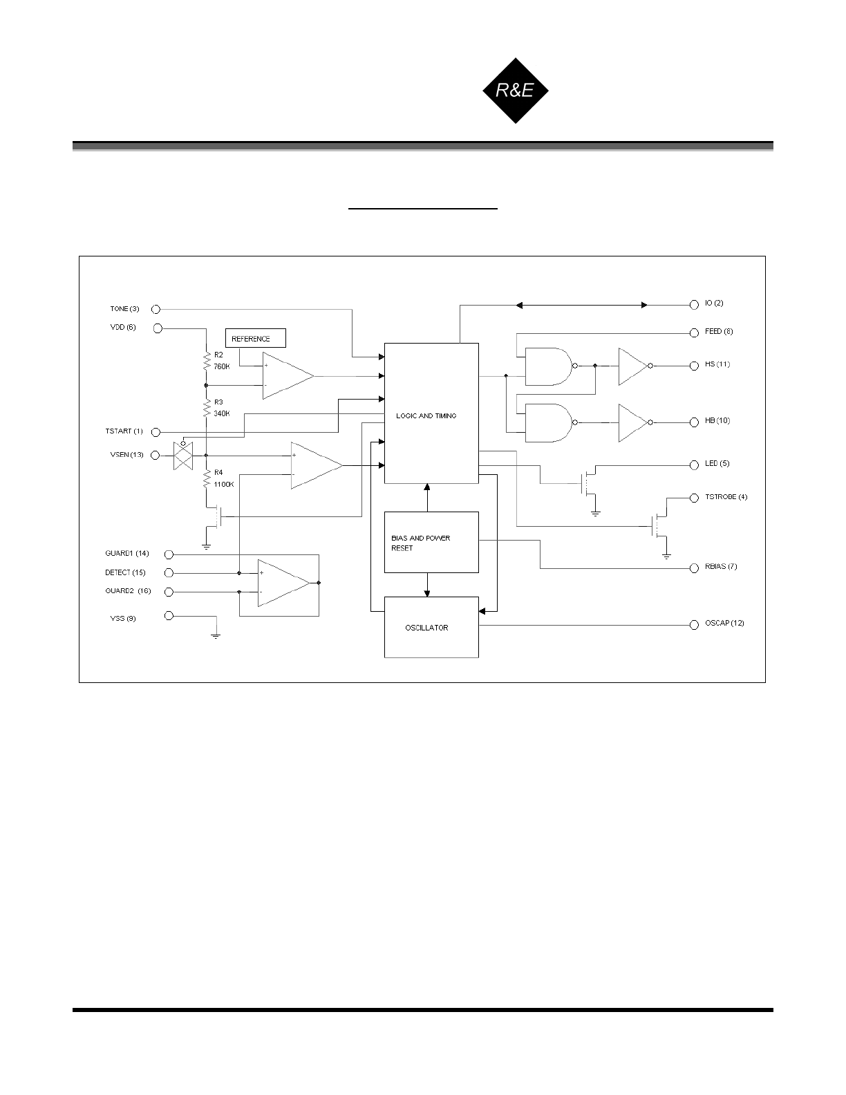
Functional Block Diagram

RE46C152
CMOS Ionization Smoke Detector ASIC with Interconnect, R&E International
Timer Mode and Tone Select
A Subsidiary of Microchip Technology
Inc.
Product Specification
© 2009 Microchip Technology Inc.
DS22175A-page 6
DEVICE DESCRIPTION and APPLICATION NOTES
Internal Timing – With external components as indicated on the application drawing the period of the oscillator is
nominally 1.67 seconds in standby. Every 1.66 seconds the detection circuitry is powered up for 10.5mS and the status
of the smoke comparator is latched. In addition every 40 seconds the LED driver is turned on for 10.5mS and the status
of the low battery comparator is latched. The smoke comparator status is not checked during the low battery test, during
the low battery horn warning chirp, or when the horn is on due to an alarm condition.
If an alarm condition is detected the oscillator period increases to 41.5mS.
Due to the low currents used in the oscillator the capacitor on pin 12 should be a low leakage type. Oscillator accuracy
will depend mainly on the tolerance of the RBIAS resistor and OSCAP capacitor.
Smoke Detection Circuit – The smoke comparator compares the ionization chamber voltage to a voltage derived from a
resistor divider across VDD. This divider voltage is available externally on pin 13 (VSEN). When smoke is detected this
voltage is internally increased by 130mV nominal to provide hysteresis and make the detector less sensitive to false
triggering.
Pin 13 (VSEN) can be used to modify the internal set point for the smoke comparator by use of external resistors to
VDD or VSS. Nominal values for the internal resistor divider are indicated on the block diagram. These internal resistor
values can vary by up to ±20% but the resistor matching should be <2% on any one device.
The guard amplifier and outputs are always active and will be within 50mV of the DETECT input to reduce surface
leakage. The guard outputs also allow for measurement of the DETECT input without loading the ionization chamber.
Low Battery Detection - An internal reference is compared to the voltage divided VDD supply. The battery can be
checked under load via the LED low side driver output since low battery status is latched at the end of the 10.5mS LED
pulse. A Transmission switch on VSEN prevents any interaction from external adjustment resistance during the low
battery test
LED Pulse – The LED is pulsed on for 10.5mS every 40S in standby. In alarm the LED is pulsed on for 10.5mS every
1S.
Interconnect – Pin 2 (IO) provides the capability to common many detectors in a single system. If a single unit goes into
alarm the IO pin is driven high. This high signal causes the interconnected units to alarm. The LED flashes every 1S for
10.5mS on the signaling unit and is inhibited on the units that are in alarm due to the IO signal. An internal sink device
on the IO pin helps to discharge the interconnect line. This charge dump device is active for 1 clock cycle after the unit
exits the alarm condition (1.67S).
The interconnect input has a 500mS nominal digital filter. This allows for interconnection to other types of alarms
(carbon monoxide for example) that may have a pulsed interconnect signal.
Testing – At power up all internal registers are reset. The low battery set point can be tested at power up by holding
FEED and OSCAP low at power up. HB will change state as VDD passes through the low battery set point. By holding
pin 12 (OSCAP) low the internal power strobe is active. Functional testing can be accelerated by driving pin 12 with a
4kHZ square wave however the 10.5mS strobe period must be maintained for proper operation of the analog circuitry.
Please refer to the timing diagrams.
Timer Mode – The transition of pin 1 (TSTART) from a high to low level initiates an eight minute timer. During this 8
minute period the open drain NMOS on pin 4 (TSTROBE) is strobed on with the internal clock. A resistor connected to
this pin could be used to modify the detector sensitivity for the timer period.
Horn Tone – Pin 3 selects the NFPA72 horn tone (high or floating) or the 2/3 duty cycle continuous tone (low).
If this pin
is externally connected high, use a current limiting resistor from pin 3 to VDD.
Reverse Battery Protection – The RE46c152 internally limits the current from VSS to VDD in the event of accidental
polarity reversal. If an input is connected to VDD it should be done through a resistance of at least 1.5K to limit the
reverse current through this path.
RE46C152
CMOS Ionization Smoke Detector ASIC with Interconnect, R&E International
Timer Mode and Tone Select
A Subsidiary of Microchip Technology
Inc.
Product Specification
© 2009 Microchip Technology Inc.
DS22175A-page 7
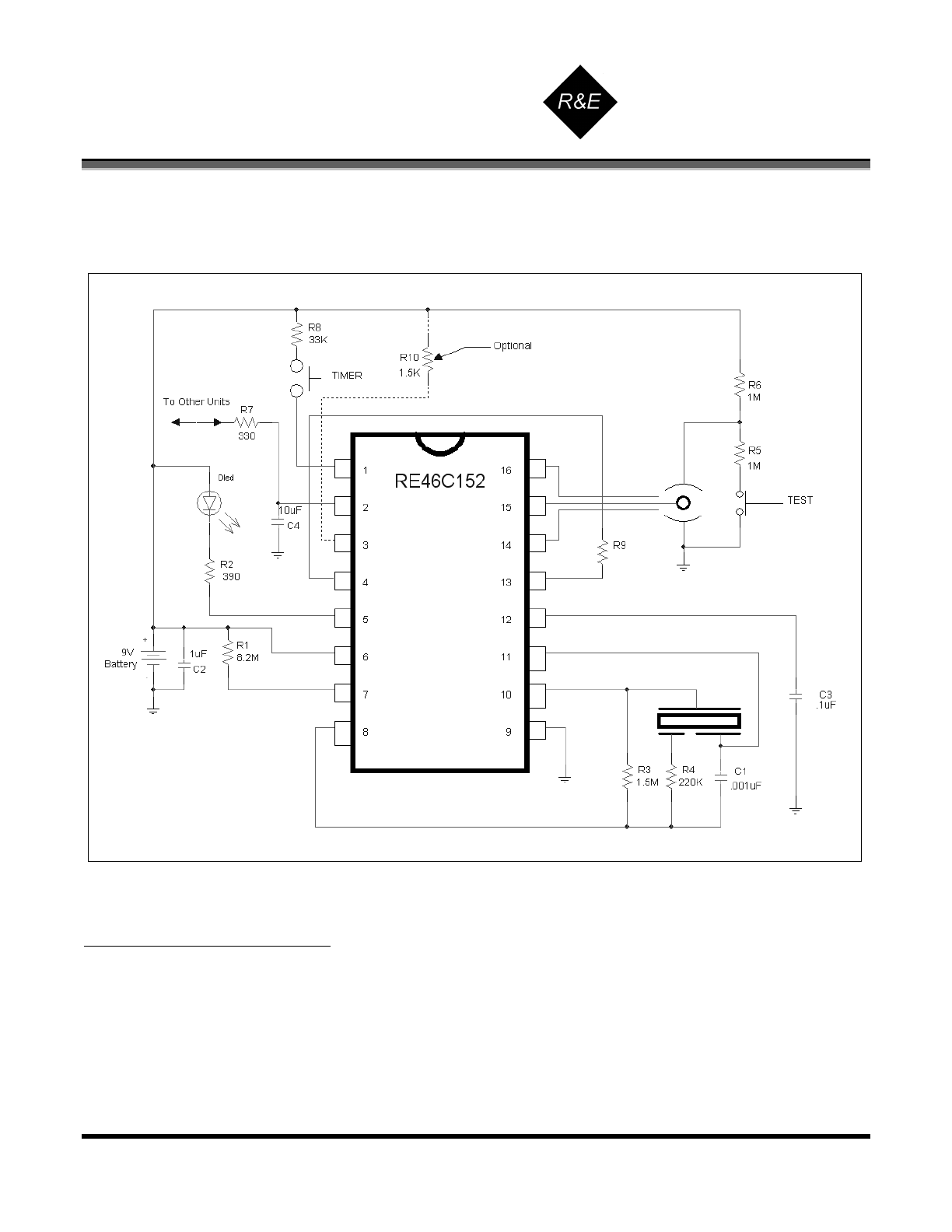
Typical Application – 2 Buttons Operation, Temporal Horn Pattern
Figure 2
Notes for Application Drawing Figure 2:
Select R9 to reduce sensitivity during the timer mode.
R3, R4 and C1 are typical values and may be adjusted to maximize sound pressure.
C2 should be located as close as possible to the device power pins.
Route the pin 8 PC board trace away from pin 7 to avoid coupling.
If used R10 is 1.5K minimum
RE46C152
CMOS Ionization Smoke Detector ASIC with Interconnect, R&E International
Timer Mode and Tone Select
A Subsidiary of Microchip Technology
Inc.
Product Specification
© 2009 Microchip Technology Inc.
DS22175A-page 8
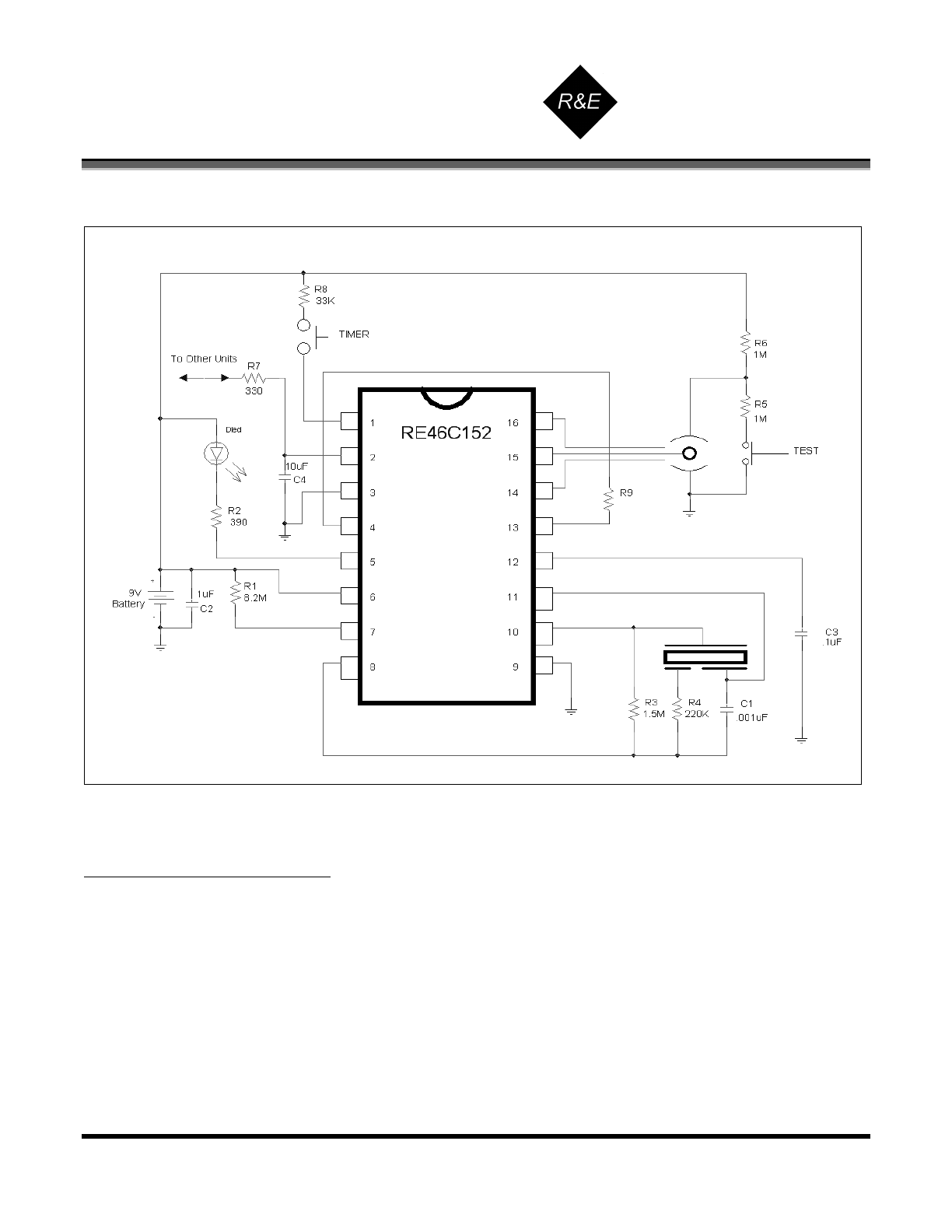
Typical Application – 1 Button Operation, Temporal Horn Pattern
Figure 3
Notes for Application Drawing Figure 3:
Select R5 and R6 values for the correct level to test the ion chamber. The voltage level at the TSTART input (pin 1) must be
greater than the minimum VIH level to initiate the timer mode. Pin 1 has an internal 180K nominal pull down which must be
considered.
Select R9 to reduce sensitivity during the timer mode.
R3, R4 and C1 are typical values and may be adjusted to maximize sound pressure.
C2 should be located as close as possible to the device power pins.
Route the pin 8 PC board trace away from pin 7 to avoid coupling.
If used R10 is 1.5K minimum
RE46C152
CMOS Ionization Smoke Detector ASIC with Interconnect, R&E International
Timer Mode and Tone Select
A Subsidiary of Microchip Technology
Inc.
Product Specification
© 2009 Microchip Technology Inc.
DS22175A-page 9
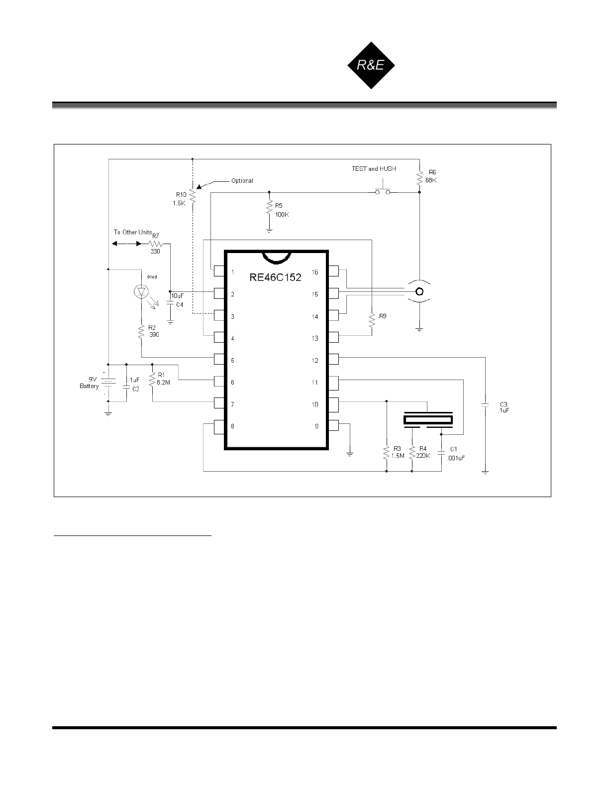
Typical Application – 2 Button Operation – 2/3 Duty Cycle Continuous Tone Horn Pattern
Figure 4
Notes for Application Drawing Figure 4:
Select R5 and R6 values for the correct level to test the ion chamber. The voltage level at the TSTART input (pin 1) must be
greater than the minimum VIH level to initiate the timer mode. Pin 1 has an internal 180K nominal pull down which must be
considered.
Select R9 to reduce sensitivity during the timer mode.
R3, R4 and C1 are typical values and may be adjusted to maximize sound pressure.
C2 should be located as close as possible to the device power pins.
Route the pin 8 PC board trace away from pin 7 to avoid coupling.
RE46C152
CMOS Ionization Smoke Detector ASIC with Interconnect, R&E International
Timer Mode and Tone Select
A Subsidiary of Microchip Technology
Inc.
Product Specification
© 2009 Microchip Technology Inc.
DS22175A-page 10
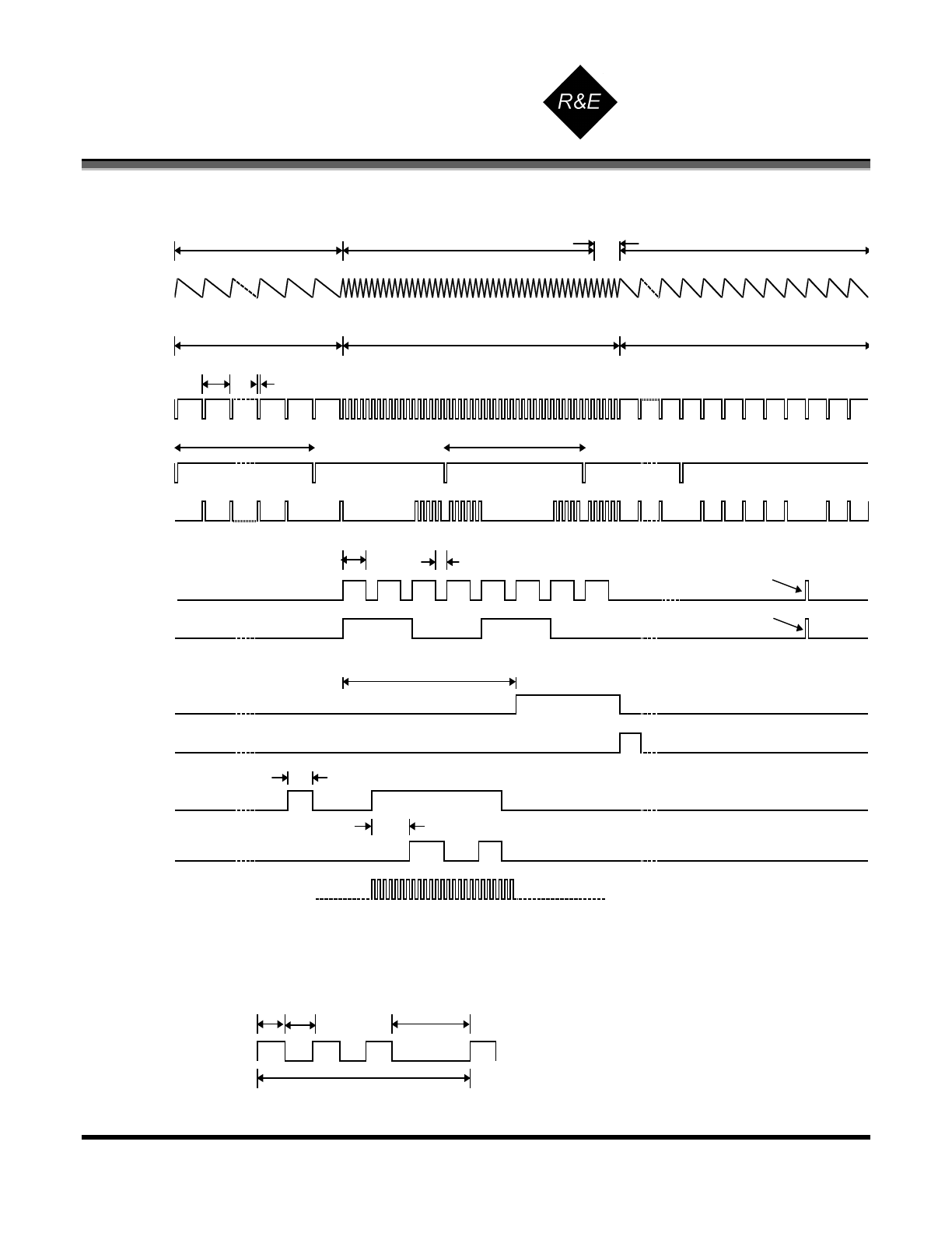
Timing Diagram (non Timer Mode)
Standby Mode; No Low Battery; No Alarm
Alarm; No Low Battery
Alarm; Low Battery
Oscillator
1.67S
10.5mS
Internal Clock
24 Clock Cycles (40 S)
LED
Sample Smoke (NFPA72)
T
HON3
T
HOF3
Low Battery Warning Chirp
Horn (2/3 Duty Cycle, TONE=VSS)
Low Battery Warning Chirp
Horn (NFPA72, TONE=Open)
See Figure Below for Complete Temporal Horn Cycle
T
IODLY1
IO (Pin 2) as Output
Timing not same scale as above
IO Charge Dump
T
IOFILT
IO ( Pin 2) as Input
LED supressed in remote alarm mode
T
IODLY2
Horn
Start of horn temporal pattern is not synchronized to an external alarm
Horn pattern not self completing for external alarm,see timing below for complete horn cycle
Internal Clock
Notes:
1. Smoke is not sampled when the horn is active. Horn cycle is self completing in local alarm.
2. Low battery warning chirp is suppressed in local or remote alarm
3. IO Dump active only in local alarm, inactive if external alarm
T
HON1
T
HOF1
Complete Temporal Horn Pattern
Pin 15 > Pin 13
Pin 13 > Pin 15; 130mV Level Shift on Pin 13
No Alarm; Low Battery
T
HOF2
24 Clock Cycles (1S)
Pin 15 > Pin 13