
2010 Microchip Technology Inc.
DS22245A-page 1
RE46C162/163
Features
• Pin Selectable Horn Patterns
• Alarm Memory
• Sensitivity Control Timer:
- 8 minute Timer for RE46C162
- 1 minute Timer for RE46C163
• >1500V ESD Protection (HBM) on All Pins
• Guard Outputs for Ion Detector Input
• ±0.75 pA Detect Input Current
• Internal Reverse Battery Protection
• Low Quiescent Current Consumption (<6.5 µA)
• I/O Filter and Charge Dump
• Internal Low Battery Detection
• Power-up Low Battery Test
• Interconnect up to 66 Detectors
• RoHS Compliant, Lead Free Packaging
Description
The RE46C162/163 devices are low-power, CMOS
ionization type, smoke detector ICs. With few external
components, these circuits will provide all the required
features for an ionization type smoke detector.
An internal oscillator strobes power to the smoke
detection circuitry for 10.5 ms every 1.67 seconds to
keep standby current to a minimum. A check for a low
battery condition is performed every 40 seconds when
in standby. The temporal horn pattern supports the
NFPA 72 emergency evacuation signal.
An interconnect pin allows multiple detectors to be
connected so when one unit alarms, all units will sound.
A charge dump feature will quickly discharge the inter-
connect line when exiting a local alarm. The intercon-
nect input is also digitally filtered.
An internal timer allows for a single button, push-to-test
to be used for a reduced sensitivity mode.
An alarm memory feature allows the user to determine
if the unit has previously entered a local alarm
condition.
Utilizing low-power CMOS technology, the
RE46C162/163 devices are designed for use in smoke
detectors that comply with Underwriters Laboratory
Specification UL217 and UL268.
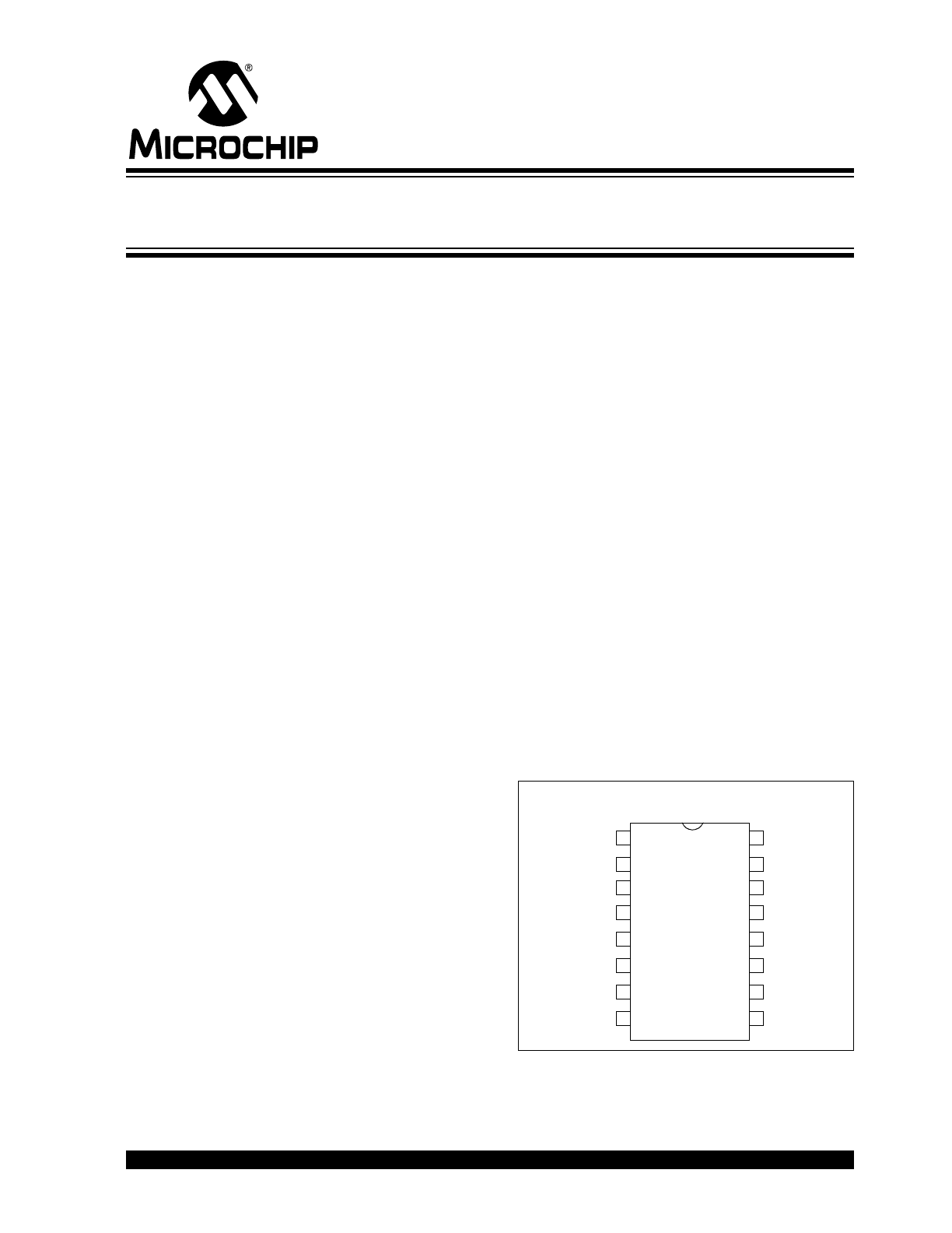
Package Types
RE46C162/163
PDIP
TSTART
1
2
3
4
5
6
7
8
16
15
14
13
12
11
10
9
IO
TONE
TSTROBE
LED
V
DD
RBIAS
FEED
GUARD2
DETECT
GUARD1
VSEN
OSCAP
HS
HB
V
SS
CMOS Ionization Smoke Detector ASIC with Interconnect,
Timer Mode and Alarm Memory
RE46C162/163
DS22245A-page 2
2010 Microchip Technology Inc.
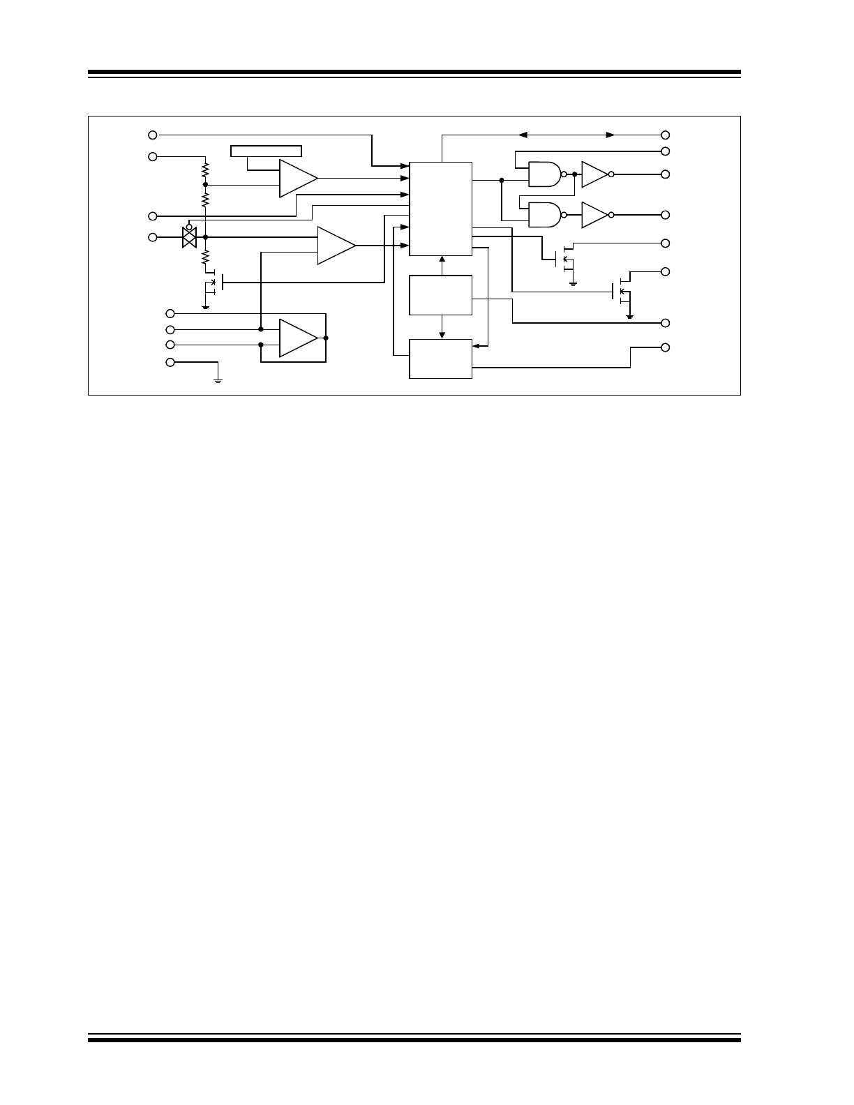
Functional Block Diagram
Logic and
Timing
Bias and
Power
Reset
Oscillator
+
-
+
-
+
-
Reference
TONE (3)
V
DD
(6)
TSTART (1)
VSEN (13)
GUARD1 (14)
DETECT (15)
GUARD2 (16)
V
SS
(9)
R4
1100K
R3
340K
R2
760K
IO
(2)
FEED (8)
HS (11)
LED (5)
TSTROBE (4)
RBIAS (7)
OSCAP (12)
HB (10)
Smoke
Comparator
Low Battery
Comparator
Guard Amp
2010 Microchip Technology Inc.
DS22245A-page 3
RE46C162/163
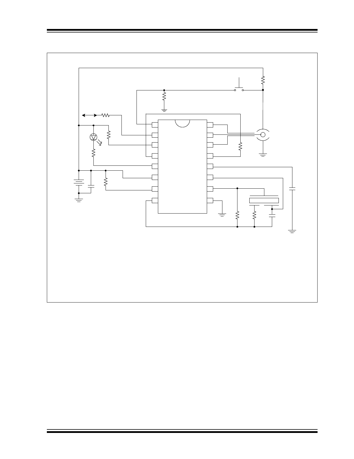
Typical Applications
Note 1:
Select R5 and R6 for the correct level to test the ion chamber. The voltage level on pin 1 (TSTART) must
be greater than the VIH level to initiate the timer. Pin 1 has an internal 180K nominal pull down which must
be considered.
2:
Select R9 to reduce sensitivity during the timer mode.
3:
R3, R4 and C1 are typical values and may be adjusted to maximize sound pressure.
4:
C2 should be located as close as possible to the device power pins.
5:
Route the pin 8 PC board trace away from pin 7 to avoid coupling.
6:
R8 should be at least 1.5K.
RE46C162 Typical Application – Temporal Horn Pattern
9V
Battery
+
-
1 µF
C2
R1
8.2M
R2
390
R8
1.5K
R7
100
To Other
Units
R5
100K
TEST and HUSH
R6
68K
R9
R4
220K
R3
1.5M
C1
.001 µF
C3
.1 µF
Dled
1
2
14
15
16
9
3
4
6
7
8
5
11
10
12
13
TSTART
TONE
IO
LED
V
DD
RBIAS
TSTROBE
FEED
GUARD2
GUARD1
DETECT
OSCAP
HS
HB
VSEN
V
SS
RE46C162/163
DS22245A-page 4
2010 Microchip Technology Inc.
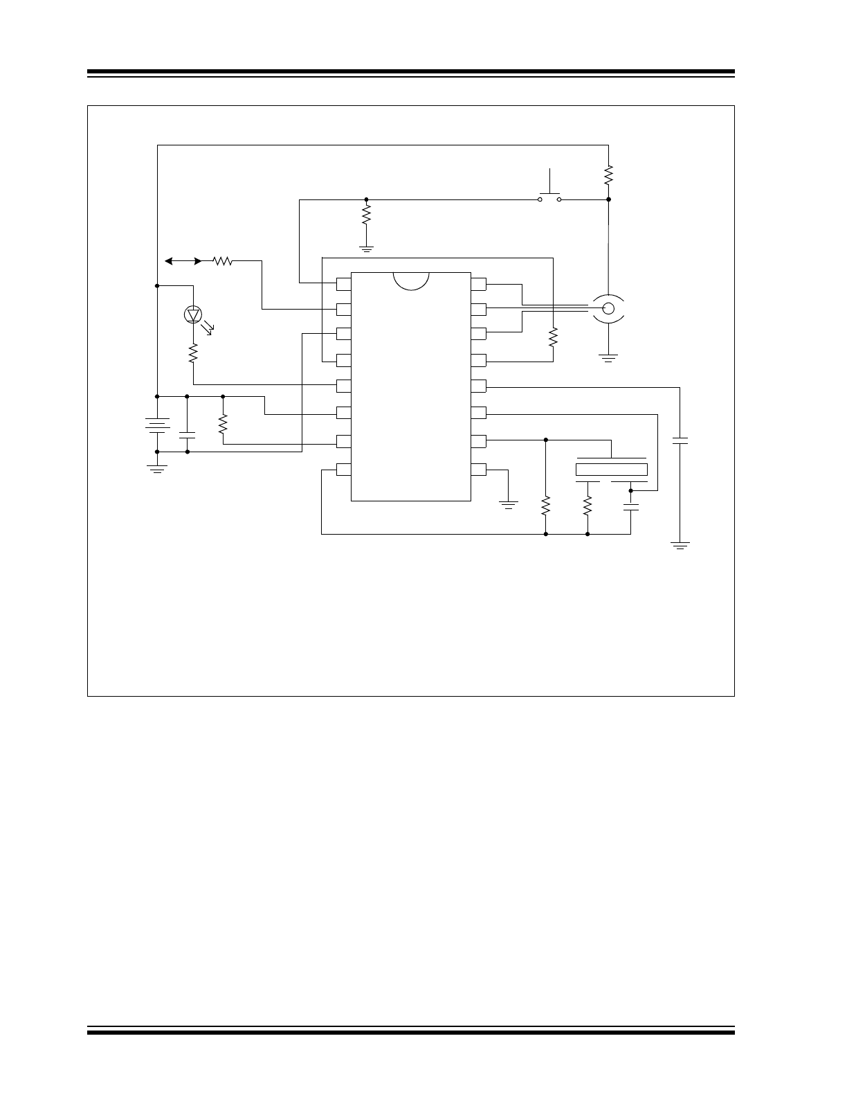
Note 1:
Select R5 and R6 for the correct level to test the ion chamber. The voltage level on pin 1 (TSTART) must be
greater than the VIH level to initiate the timer. Pin 1 has an internal 180K nominal pull down which must be
considered.
2:
Select R9 to reduce sensitivity during the timer mode.
3:
R3, R4 and C1 are typical values and may be adjusted to maximize sound pressure.
4:
C2 should be located as close as possible to the device power pins.
5:
Route the pin 8 PC board trace away from pin 7 to avoid coupling.
RE46C162 Typical Application – 2/3 Duty Cycle Continuous Tone Horn Pattern
9V
Battery
+
-
1 µF
C2
R1
8.2M
R2
390
R7
100
To Other
Units
R5
100K
TEST and HUSH
R6
68K
R9
R4
220K
R3
1.5M
C1
.001 µF
C3
.1 µF
Dled
1
2
14
15
16
9
3
4
6
7
8
5
11
10
12
13
TSTART
TONE
IO
LED
V
DD
RBIAS
TSTROBE
FEED
GUARD2
GUARD1
DETECT
OSCAP
HS
HB
VSEN
V
SS
2010 Microchip Technology Inc.
DS22245A-page 5
RE46C162/163
1.0
ELECTRICAL
CHARACTERISTICS
Absolute Maximum Ratings†
V
DD
....................................................................................15V
Input Voltage Range Except FEED, I/O ........... V
IN
=-.3V to V
DD
+.3V
FEED Input Voltage Range .................... V
INFD
= -10 to +22V
I/O Input Voltage Range................................V
IO1
= -.3 to 15V
Reverse Battery Time ...............................................T
RB
= 5S
Input Current except FEED................................... I
IN
= 10 mA
Operating Temperature ............................... T
A
= -10 to +60°C
Storage Temperature ............................T
STG
= -55 to +125°C
Maximum Junction Temperature......................... T
J
= +150°C
† Notice:
Stresses above those listed under “Maximum rat-
ings” may cause permanent damage to the device. This is a
stress rating only and functional operation of the device at
these or any other conditions above those indicated in the
operation listings of this specification is not implied. Exposure
to maximum rating conditions for extended periods may affect
device reliability.
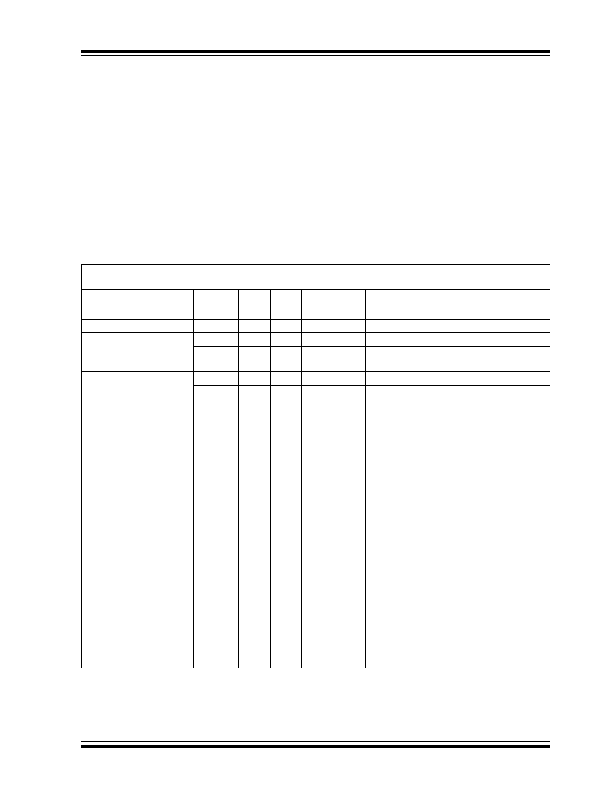
DC ELECTRICAL CHARACTERISTICS
DC Electrical Characteristics:
Unless otherwise indicated, all parameters apply at T
A
= +25°C, V
DD
= 9V,
OSCAP = .1 µF, RBIAS = 8.2 M
, V
SS
= 0V
Parameter
Symbol
Test
Pin
Min
Typ
Max
Units
Conditions
Supply Voltage
V
DD
6
6
—
12
V
Operating
Supply Current
I
DD1
6
—
5
6.5
µA
RBIAS = 8.2 MW, OSCAP = .1 µF
I
DD2
6
—
—
9
µA
RBIAS = 8.2 MW, OSCAP = .1 µF;
V
DD
= 12V
Input Voltage High
V
IH1
3,8
6.2
4.5
—
V
Note 2
V
IH2
2
3
—
—
V
No local alarm, I/O as an input
V
IH3
1
4.5
—
—
V
Input Voltage Low
V
IL1
3,8
—
4.5
2.7
V
Note 2
V
IL2
2
—
—
1
V
No local alarm, I/O as an input
V
IL3
1
—
—
2.5
V
Input Leakage Low
IL
DET1
15
—
—
-0.75
pA
V
DD
= 9V, DETECT = V
SS
,
0-40% RH
IL
DET2
15
—
—
-1.50
pA
V
DD
= 9V, DETECT = V
SS
, 85%
RH Note 1
IL
FD
8
—
—
-50
µA
FEED = -10V
IL
TONE
3
—
—
-100
nA
TONE = V
SS
Input Leakage High
IH
DET1
15
—
—
0.75
pA
V
DD
= 9V, DETECT = V
DD
,
0-40% RH
IH
DET2
15
—
—
1.50
pA
V
DD
= 9V, DETECT = V
DD
,
85% RH Note 1
IH
FD
8
—
—
50
µA
FEED = 22V
I
IOL2
2
—
—
150
µA
No alarm, V
IO
= 15V
IH
TONE
3
—
—
100
nA
TONE = V
DD
Output Off Leakage High
I
IOHZ
4,5
—
—
1
µA
Outputs off
Input Pull Down Current
I
PD1
1
20
50
80
µA
TSTART = 9V
Output High Voltage
V
OH1
10,11
6.3
—
—
V
I
OH
= -16 mA, V
DD
= 7.2V
Note
1:
Sample test only.
2:
Not 100% production tested.
3:
Production test at room with temperature guard banded limits.
RE46C162/163
DS22245A-page 6
2010 Microchip Technology Inc.
Output Low Voltage
V
OL1
10,11
—
—
.9
V
I
OL
= 16 mA, V
DD
= 7.2V
V
OL2
4
—
—
.5
V
I
OL
= 500 µA
V
OL3
5
—
—
1
V
I
OL
= 10 mA, V
DD
= 7.2V
Output Current
I
IOL1
2
25
—
60
µA
No alarm, V
IO
= V
DD
-2V
I
IOH1
2
-4
—
-16
mA
Alarm, V
IO
= V
DD
-2V or V
IO
= 0V
I
IODMP
2
5
—
—
mA
At conclusion of local alarm or test,
V
IO
= 1V
Low Battery Voltage
V
LB
6
7.2
7.5
7.8
V
T
A
= -10 to +60ºC, Note 3
Internal Sensitivity Set
Voltage
V
SET1
13
48.5
50
51.5
%V
DD
Offset Voltage
VG
OS1
14,15
-50
—
50
mV
Guard amplifier
VG
OS2
15,16
-50
—
50
mV
Guard amplifier
VG
OS3
13,15
-50
—
50
mV
Smoke comparator
Common Mode Voltage
V
CM1
14,15
2
—
V
DD
-
.5
V
Guard amplifier, Note 2
V
CM2
13,15
.5
—
V
DD
-2
V
Smoke comparator, Note 2
Output Impedance
Z
OUT
14,16
—
10
—
kW
Guard amplifier outputs, Note 2
Hysteresis
V
HYS
13
90
130
170
mV
No alarm to alarm condition
DC ELECTRICAL CHARACTERISTICS (CONTINUED)
DC Electrical Characteristics:
Unless otherwise indicated, all parameters apply at T
A
= +25°C, V
DD
= 9V,
OSCAP = .1 µF, RBIAS = 8.2 M
, V
SS
= 0V
Parameter
Symbol
Test
Pin
Min
Typ
Max
Units
Conditions
Note
1:
Sample test only.
2:
Not 100% production tested.
3:
Production test at room with temperature guard banded limits.
AC ELECTRICAL CHARACTERISTICS
AC Electrical Characteristics:
Unless otherwise indicated, all parameters apply at T
A
= +25°C, V
DD
= 9V,
OSCAP = .1 µF, RBIAS = 8.2 M
, V
SS
= 0V.
Parameter
Symbol
Test
Pin
Min
Typ
Max
Units
Conditions
Oscillator Period
T
PER1
12
1.34
1.67
2
s
No alarm condition
T
PER2
12
37.5
41.7
45.8
ms
Alarm condition
Oscillator Pulse Width
T
PW
5
9.4
10.5
12.9
ms
Operating
LED On Time
T
LON
5
9.4
10.5
12.9
ms
Operating
LED Off Time
T
LOF1
5
32
40
48
s
Standby, no alarm
T
LOF2
5
.9
1
1.1
s
Alarm condition
T
LOF3
5
8
10
12
s
Timer mode, no alarm
T
LOF4
5
2.66
3.33
4
s
Alarm memory LED pulse spacing
T
LOF5
5
26
33.3
40
s
Alarm memory LED off time between
pulse train
Note 1:
See timing diagram for horn temporal and non-temporal patterns.
2:
T
PER1
,T
PER2
and T
PW
are 100% production tested. All other timing is verified by functional testing.
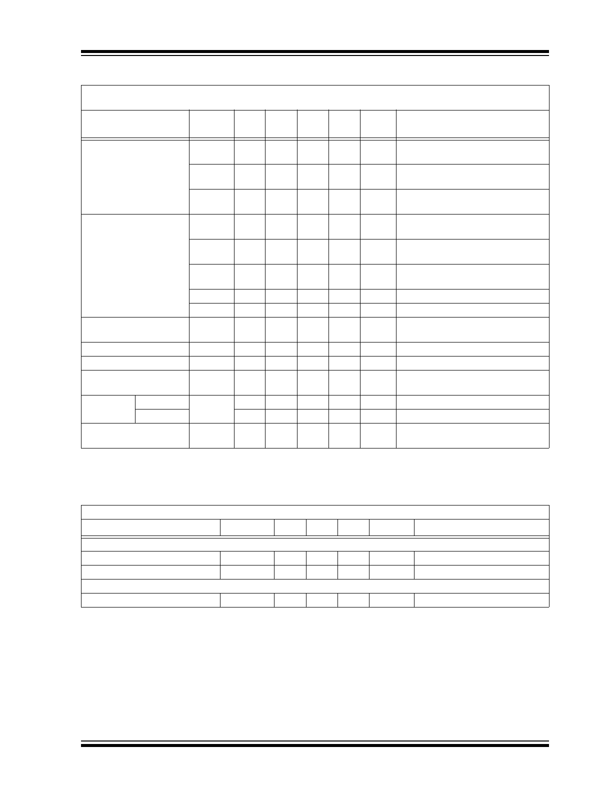
2010 Microchip Technology Inc.
DS22245A-page 7
RE46C162/163
Horn On Time
T
HON1
10,11
450
500
550
ms
Operating, alarm condition, Note 1,
TONE = High
T
HON2
10,11
9.4
10.5
12.9
ms
Low battery, no alarm or PTT in
alarm memory
T
HON3
10,11
150
167
183
ms
Operating, alarm condition, Note 1,
TONE = Low
Horn Off Time
T
HOF1
10,11
450
500
550
ms
Operating, alarm condition, Note 1,
TONE = High
T
HOF2
10,11
1.35
1.5
1.65
s
Operating, alarm condition, Note 1,
TONE = High
T
HOF3
10,11
75
83
92
ms
Operating, alarm condition, Note 1,
TONE = Low
T
HOF4
10,11
32
40
48
s
Low battery, no alarm
T
HOF5
10,11
216
240
264
ms
PTT in alarm memory
I/O Charge
Dump Duration
T
IODMP
2
1.34
1.67
2.0
s
At conclusion of local alarm or test
I/O Delay
T
IODLY1
2
—
3
—
s
From start of local alarm to I/O active
I/O Filter
T
IOFILT
2
—
—
450
ms
I/O as input, no local alarm
Remote Alarm Delay
T
IODLY2
2
.450
—
2.75
s
No local alarm, I/O as input,
from I/O active to horn active
Timer
Period
RE46C162
T
TPER
4
6
8
10
Min
No alarm
RE46C163
4
40
50
60
s
No alarm
Alarm Memory
Visual Indicator Period
T
AMTPER
5
19.2
24
28.8
Hour
No alarm, alarm memory
TEMPERATURE CHARACTERISTICS
Electrical Specifications: Unless otherwise indicated,
Parameters
Sym
Min
Typ
Max
Units
Conditions
Temperature Ranges
Operating Temperature Range
T
A
-10
—
+60
°C
Storage Temperature Range
T
STG
-55
—
+125
°C
Thermal Package Resistances
Thermal Resistance, 16L-PDIP
θJ
A
—
70
—
°C/W
AC ELECTRICAL CHARACTERISTICS (CONTINUED)
AC Electrical Characteristics:
Unless otherwise indicated, all parameters apply at T
A
= +25°C, V
DD
= 9V,
OSCAP = .1 µF, RBIAS = 8.2 M
, V
SS
= 0V.
Parameter
Symbol
Test
Pin
Min
Typ
Max
Units
Conditions
Note 1:
See timing diagram for horn temporal and non-temporal patterns.
2:
T
PER1
,T
PER2
and T
PW
are 100% production tested. All other timing is verified by functional testing.

RE46C162/163
DS22245A-page 8
2010 Microchip Technology Inc.
NOTES:
2010 Microchip Technology Inc.
DS22245A-page 9
RE46C162/163
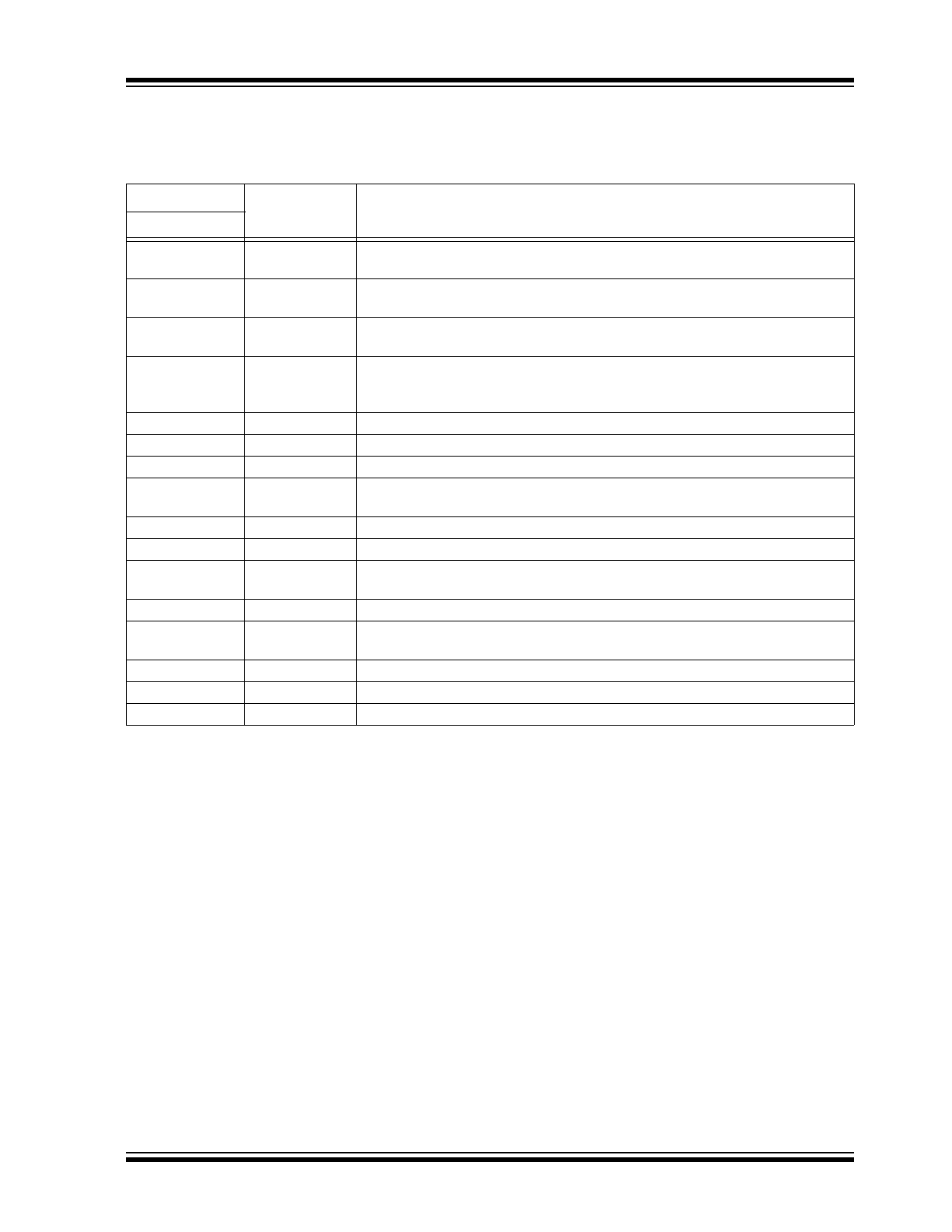
2.0
PIN DESCRIPTIONS
The descriptions of the pins are listed in
Table 2-1
.
TABLE 2-1:
PIN FUNCTION TABLE
RE46C162/163
Name
Description
PDIP, SOIC
1
TSTART
This input is used to invoke the push-to-test alarm, alarm memory indication,
and the timer mode. This input has an internal pull-down.
2
I/O
This bidirectional pin provides the capability to interconnect many detectors in a
single system. This pin has an internal pull-down.
3
TONE
This pin selects the NFPA72 horn tone (high) or the 2/3 duty cycle continuous
tone (low).
4
TSTROBE
This pin is strobed on with the internal clock in timer mode. A resistor
connected to this pin is used to modify the detector sensitivity for the timer
period.
5
LED
Open drain NMOS output used to drive a visible LED.
6
V
DD
Connect to the positive supply voltage.
7
RBIAS
A resistor connected between this pin and V
DD
sets the internal bias current.
8
FEED
Usually connected to the feedback electrode through a current limiting resistor.
If not used, this pin must be connected to V
DD
or V
SS
.
9
V
SS
Connect to the negative supply voltage.
10
HB
This pin is connected to the metal electrode of a piezoelectric transducer.
11
HS
HS is a complementary output to HB and connects to the ceramic electrode of
the piezoelectric transducer.
12
OSCAP
A capacitor connected between this pin and V
SS
sets the oscillator timing.
13
VSEN
This pin can be used to modify the set point for the smoke comparator by use of
external resistors to V
DD
or V
SS
.
14
GUARD1
Output of the guard amplifier.
15
DETECT
Connect to the collector electrode (CEV) of the ion smoke chamber.
16
GUARD2
Output of the guard amplifier.

RE46C162/163
DS22245A-page 10
2010 Microchip Technology Inc.
NOTES: