

2015 Microchip Technology Inc.
DS00001623B-page 1
General Description
The CAP1126, which incorporates RightTouch
®
tech-
nology, is a multiple channel Capacitive Touch sensor
with multiple power LED drivers. It contains six (6) indi-
vidual capacitive touch sensor inputs with programma-
ble sensitivity for use in touch sensor applications.
Each sensor input automatically recalibrates to com-
pensate for gradual environmental changes.
The CAP1126 also contains two (2) LED drivers that
offer full-on / off, variable rate blinking, dimness con-
trols, and breathing. Each of the LED drivers may be
linked to one of the sensor inputs to be actuated when
a touch is detected. As well, each LED driver may be
individually controlled via a host controller.
The CAP1126 includes Multiple Pattern Touch recogni-
tion that allows the user to select a specific set of but-
tons to be touched simultaneously. If this pattern is
detected, then a status bit is set and an interrupt gen-
erated.
Additionally, the CAP1126 includes circuitry and sup-
port for enhanced sensor proximity detection.
The CAP1126 offers multiple power states operating at
low quiescent currents. In the Standby state of opera-
tion, one or more capacitive touch sensor inputs are
active and all LEDs may be used. If a touch is detected,
it will wake the system using the WAKE/SPI_MOSI pin.
Deep Sleep is the lowest power state available, draw-
ing 5uA (typical) of current. In this state, no sensor
inputs are active. Driving the WAKE/SPI_MOSI pin or
communications will wake the device.
Applications
• Desktop and Notebook PCs
• LCD Monitors
• Consumer Electronics
• Appliances
Features
• Six (6) Capacitive Touch Sensor Inputs
- Programmable sensitivity
- Automatic recalibration
- Individual thresholds for each button
• Proximity Detection
• Multiple Button Pattern Detection
• Calibrates for Parasitic Capacitance
• Analog Filtering for System Noise Sources
• Press and Hold feature for Volume-like Applica-
tions
• Multiple Communication Interfaces
- SMBus / I
2
C compliant interface
- SPI communications
- Pin selectable communications protocol and
multiple slave addresses (SMBus / I
2
C only)
• Low Power Operation
- 5uA quiescent current in Deep Sleep
- 50uA quiescent current in Standby (1 sensor
input monitored)
- Samples one or more channels in Standby
• Two (2) LED Driver Outputs
- Open Drain or Push-Pull
- Programmable blink, breathe, and dimness
controls
- Can be linked to Capacitive Touch Sensor
inputs
• Dedicated Wake output flags touches in low
power state
• System RESET pin
• Available in 16-pin 4mm x 4mm RoHS compliant
QFN package
CAP1126
6 Channel Capacitive Touch Sensor with 2 LED Drivers

CAP1126
DS00001623B-page 2
2015 Microchip Technology Inc.
TO OUR VALUED CUSTOMERS
It is our intention to provide our valued customers with the best documentation possible to ensure successful use of your Microchip
products. To this end, we will continue to improve our publications to better suit your needs. Our publications will be refined and
enhanced as new volumes and updates are introduced.
If you have any questions or comments regarding this publication, please contact the Marketing Communications Department via
E-mail at
docerrors@microchip.com
. We welcome your feedback.
Most Current Data Sheet
To obtain the most up-to-date version of this data sheet, please register at our Worldwide Web site at:
http://www.microchip.com
You can determine the version of a data sheet by examining its literature number found on the bottom outside corner of any page.
The last character of the literature number is the version number, (e.g., DS30000000A is version A of document DS30000000).
Errata
An errata sheet, describing minor operational differences from the data sheet and recommended workarounds, may exist for cur-
rent devices. As device/documentation issues become known to us, we will publish an errata sheet. The errata will specify the
revision of silicon and revision of document to which it applies.
To determine if an errata sheet exists for a particular device, please check with one of the following:
• Microchip’s Worldwide Web site;
http://www.microchip.com
• Your local Microchip sales office (see last page)
When contacting a sales office, please specify which device, revision of silicon and data sheet (include -literature number) you are
using.
Customer Notification System
Register on our web site at
www.microchip.com
to receive the most current information on all of our products.

2015 Microchip Technology Inc.
DS00001623B-page 3
CAP1126
Table of Contents
1.0 Block Diagram ................................................................................................................................................................................. 4
2.0 Pin Description ................................................................................................................................................................................ 5
3.0 Electrical Specifications .................................................................................................................................................................. 9
4.0 Communications ........................................................................................................................................................................... 12
5.0 General Description ...................................................................................................................................................................... 23
6.0 Register Description ...................................................................................................................................................................... 29
7.0 Package Information ..................................................................................................................................................................... 67
Appendix A: Device Delta ................................................................................................................................................................... 72
Appendix B: Data Sheet Revision History ........................................................................................................................................... 74
The Microchip Web Site ...................................................................................................................................................................... 76
Customer Change Notification Service ............................................................................................................................................... 76
Customer Support ............................................................................................................................................................................... 76
Product Identification System ............................................................................................................................................................. 77
CAP1126
DS00001623B-page 4
2015 Microchip Technology Inc.
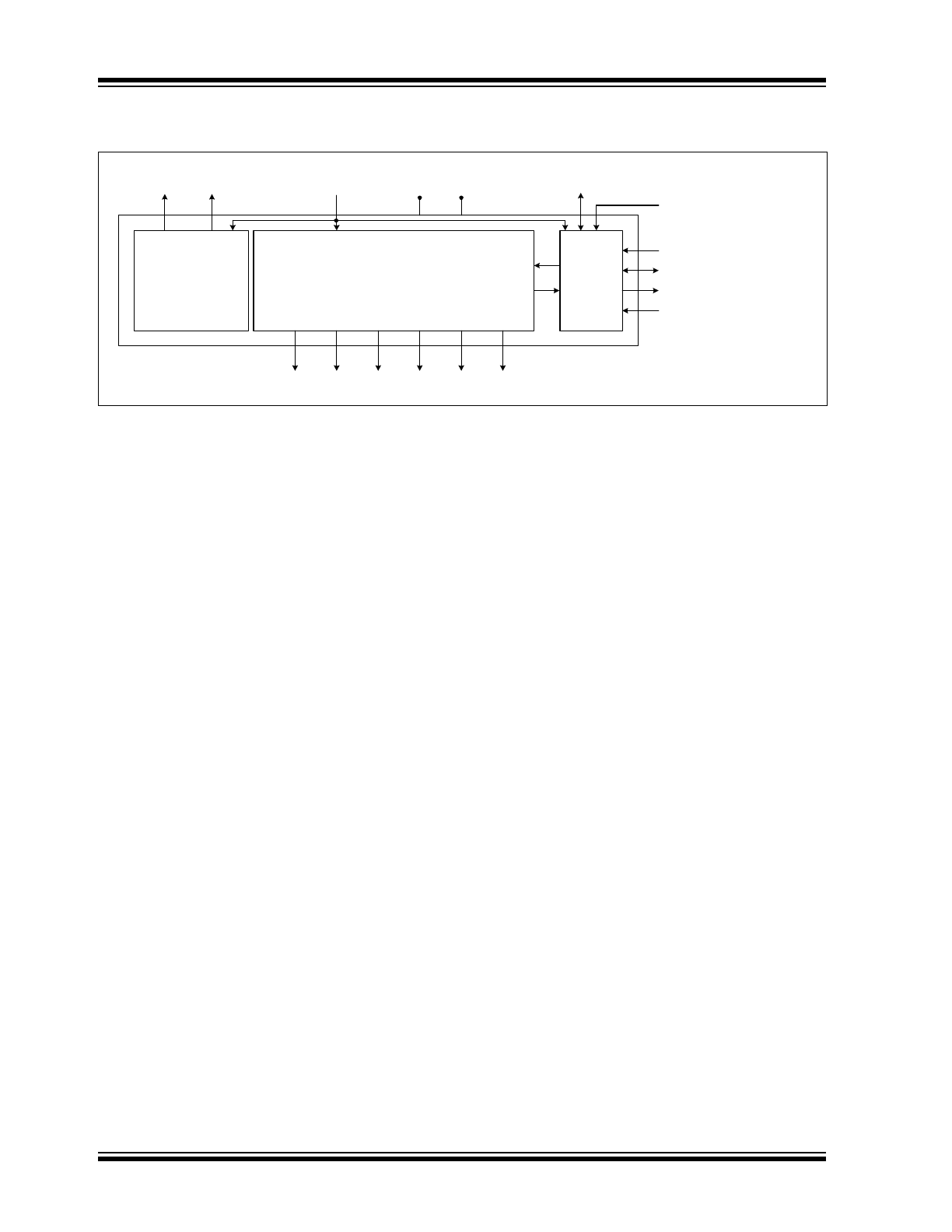
1.0
BLOCK DIAGRAM
SMBus /
BC-Link /
SPI Slave
Protocol
SMCLK BC_CLK /
SPI_CLK
SMDATA BC_DATA / SPI_MSIO /
SPI_MISO
VDD
GND
ALERT# / BC_IRQ#
Capacitive Touch Sensing Algorithm
LED1
CS1
CS2
CS3
CS4
CS5
CS6
LED Driver, Breathe, and
Dimness control
WAKE / SPI_MOSI
RESET
ADDR_COMM
SPI_CS#
LED2
2015 Microchip Technology Inc.
DS00001623B-page 5
CAP1126
2.0
PIN DESCRIPTION
FIGURE 2-1:
CAP1126 Pin Diagram (16-Pin QFN)
TABLE 2-1:
PIN DESCRIPTION FOR CAP1126
Pin
Number
Pin Name
Pin Function
Pin Type
Unused
Connection
1
SPI_CS#
Active low chip-select for SPI bus
DI (5V)
Connect to
Ground
2
WAKE / SPI_-
MOSI
WAKE - Active high wake / interrupt output
Standby power state - requires pull-down resistor
DO
Pull-down
Resistor
WAKE - Active high wake input - requires pull-down
resistor
Deep Sleep power state
DI
SPI_MOSI - SPI Master-Out-Slave-In port when used in
normal mode
DI (5V)
Connect to
Ground
1
2
3
4
12
11
10
9
16
15
14
13
5
6
7
8
SMCLK / BC_CLK /
SPI_CLK
SMDATA / BC_DATA / SPI_MSIO /
SPI_MISO
WAKE / SPI_MOSI
ADDR_COMM
VDD
CS6
SPI_CS#
CS5
CS1
CS2
CS3
RESET
LED2
LED1
CS4
AL
ERT#
/
BC_
IRQ#
CAP1126
16 pin QFN
GND

CAP1126
DS00001623B-page 6
2015 Microchip Technology Inc.
3
SMDATA /
SPI_MSIO /
SPI_MISO
SMDATA - Bi-directional, open-drain SMBus data -
requires pull-up resistor
DIOD (5V)
n/a
SPI_MSIO - SPI Master-Slave-In-Out bidirectional port
when used in bi-directional mode
DIO
SPI_MISO - SPI Master-In-Slave-Out port when used in
normal mode
DO
4
SMCLK / SPI_-
CLK
SMCLK - SMBus clock input - requires pull-up resistor
DI (5V)
n/a
SPI_CLK - SPI clock input
DI (5V)
5
LED1
Open drain LED 1 driver (default)
OD (5V)
Connect to
Ground
Push-pull LED 1 driver
DO
leave open or
connect to
Ground
6
LED2
Open drain LED 2 driver (default)
OD (5V)
Connect to
Ground
Push-pull LED 2 driver
DO
leave open or
connect to
Ground
7
RESET
Active high soft reset for system - resets all registers to
default values. If not used, connect to ground.
DI (5V)
Connect to
Ground
8
ALERT#
ALERT# - Active low alert / interrupt output for SMBus
alert or SPI interrupt
OD (5V)
Connect to
Ground
ALERT# - Active high push-pull alert / interrupt output for
SMBus alert or SPI interrupt
DO leave
open
9
ADDR_COMM
Address / communications select pin - pull-down resistor
determines address / communications mechanism
AI
n/a
10
CS6
Capacitive Touch Sensor Input 6
AIO
Connect to
Ground
11
CS5
Capacitive Touch Sensor Input 5
AIO
Connect to
Ground
12
CS4
Capacitive Touch Sensor Input 4
AIO
Connect to
Ground
13
CS3
Capacitive Touch Sensor Input 3
AIO
Connect to
Ground
14
CS2
Capacitive Touch Sensor Input 2
AIO
Connect to
Ground
15
CS1
Capacitive Touch Sensor Input 1
AIO
Connect to
Ground
16
VDD
Positive Power supply
Power
n/a
TABLE 2-1:
PIN DESCRIPTION FOR CAP1126 (CONTINUED)
Pin
Number
Pin Name
Pin Function
Pin Type
Unused
Connection
2015 Microchip Technology Inc.
DS00001623B-page 7
CAP1126
APPLICATION NOTE: When the ALERT# pinis configured as an active low output, it will be open drain. When it is
configured as an active high output, it will be push-pull.
APPLICATION NOTE: For the 5V tolerant pins that have a pull-up resistor, the pull-up voltage must not exceed 3.6V
when the CAP1126 is unpowered.
APPLICATION NOTE: The SPI_CS# pin should be grounded when SMBus, or I
2
C,communications are used.
The pin types are described in
Table 2-2
. All pins labeled with (5V) are 5V tolerant.
Bottom
Pad
GND
Ground
Power
n/a
TABLE 2-2:
PIN TYPES
Pin Type
Description
Power
This pin is used to supply power or ground to the device.
DI
Digital Input - This pin is used as a digital input. This pin is 5V tolerant.
AIO
Analog Input / Output -This pin is used as an I/O for analog signals.
DIOD
Digital Input / Open Drain Output - This pin is used as a digital I/O. When it is used as an out-
put, it is open drain and requires a pull-up resistor. This pin is 5V tolerant.
OD
Open Drain Digital Output - This pin is used as a digital output. It is open drain and requires a
pull-up resistor. This pin is 5V tolerant.
DO
Push-pull Digital Output - This pin is used as a digital output and can sink and source current.
DIO
Push-pull Digital Input / Output - This pin is used as an I/O for digital signals.
TABLE 2-1:
PIN DESCRIPTION FOR CAP1126 (CONTINUED)
Pin
Number
Pin Name
Pin Function
Pin Type
Unused
Connection

CAP1126
DS00001623B-page 8
2015 Microchip Technology Inc.
3.0
ELECTRICAL SPECIFICATIONS
Note 3-1
Stresses above those listed could cause permanent damage to the device. This is a stress rating
only and functional operation of the device at any other condition above those indicated in the
operation sections of this specification is not implied.
Note 3-2
For the 5V tolerant pins that have a pull-up resistor, the voltage difference between V
5VT_PIN
and V
DD
must never exceed 3.6V.
Note 3-3
The Package Power Dissipation specification assumes a recommended thermal via design consisting
of a 3x3 matrix of 0.3mm (12mil) vias at 1.0mm pitch connected to the ground plane with a 2.1mm
x 2.1mm thermal landing.
Note 3-4
Junction to Ambient (
θ
JA
) is dependent on the design of the thermal vias. Without thermal vias and
a thermal landing, the
θ
JA
is approximately 60°C/W including localized PCB temperature increase.
TABLE 3-1:
ABSOLUTE MAXIMUM RATINGS
Voltage on 5V tolerant pins (V
5VT_PIN
)
-0.3 to 5.5
V
Voltage on 5V tolerant pins (|V
5VT_PIN
- V
DD
|)
Note 3-2
0 to 3.6
V
Voltage on VDD pin
-0.3 to 4
V
Voltage on any other pin to GND
-0.3 to VDD + 0.3
V
Package Power Dissipation up to T
A
= 85°C for 16 pin QFN
(see
Note 3-3
)
0.9
W
Junction to Ambient (
θ
JA
) (see
Note 3-4
)
58
°C/W
Operating Ambient Temperature Range
-40 to 125
°C
Storage Temperature Range
-55 to 150
°C
ESD Rating, All Pins, HBM
8000
V
2015 Microchip Technology Inc.
DS00001623B-page 9
CAP1126
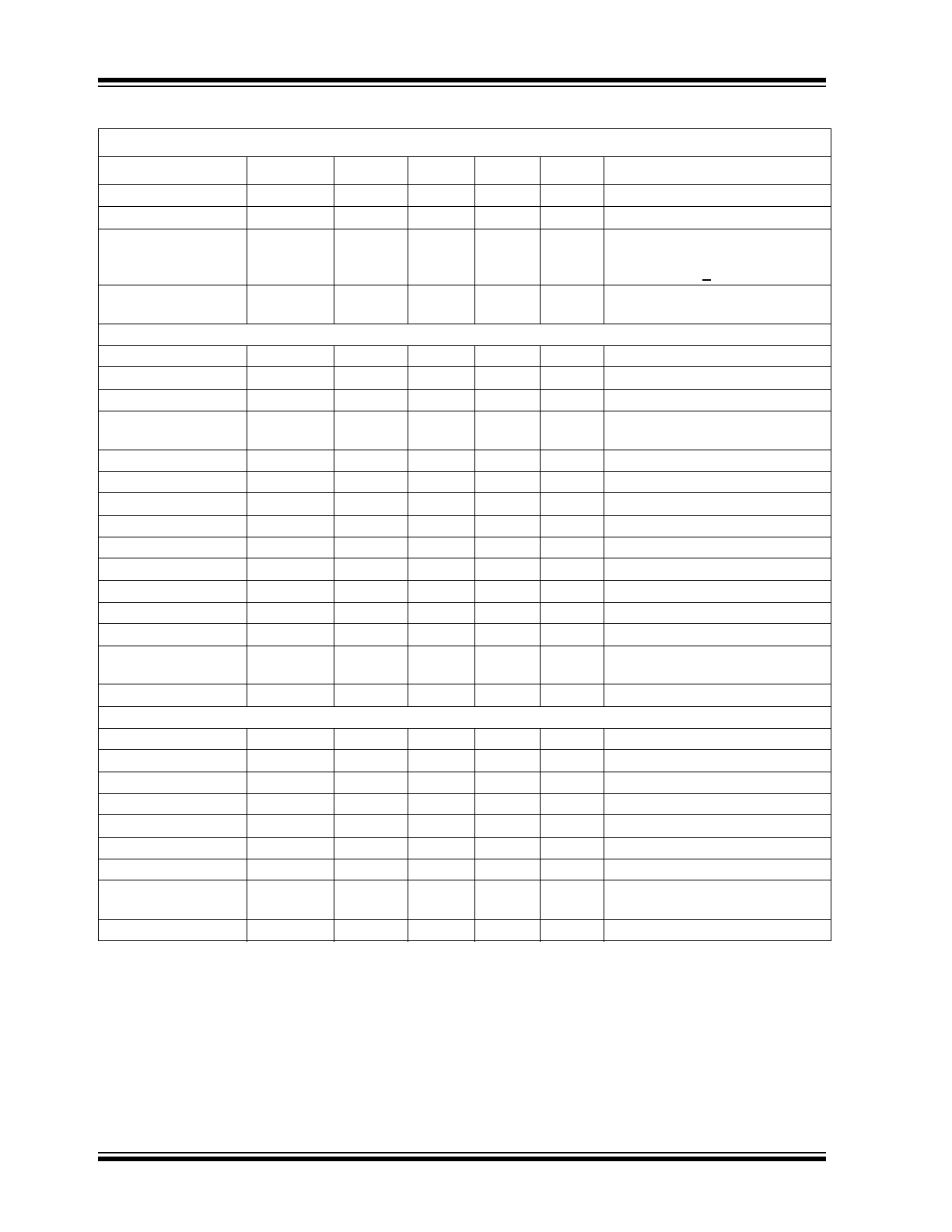
TABLE 3-2:
ELECTRICAL SPECIFICATIONS
V
DD
= 3V to 3.6V, T
A
= 0°C to 85°C, all typical values at T
A
= 27°C unless otherwise noted.
Characteristic
Symbol
Min
Typ
Max
Unit
Conditions
DC Power
Supply Voltage
V
DD
3.0
3.3
3.6
V
Supply Current
I
STBY
120
170
uA
Standby state active
1 sensor input monitored
No LEDs active
Default conditions (8 avg, 70ms
cycle time)
I
STBY
50
uA
Standby state active
1 sensor input monitored
No LEDs active
1 avg, 140ms cycle time,
I
DSLEEP
5
15
uA
Deep Sleep state active
LEDs at 100% or 0% Duty Cycle
No communications
T
A
< 40°C
3.135 < V
DD
< 3.465V
I
DD
500
600
uA
Capacitive Sensing Active
No LEDs active
Capacitive Touch Sensor Inputs
Maximum Base
Capacitance
C
BASE
50
pF
Pad untouched
Minimum Detectable
Capacitive Shift
Δ
C
TOUCH
20
fF
Pad touched - default conditions (1
avg, 35ms cycle time, 1x sensitiv-
ity)
Recommended Cap
Shift
Δ
C
TOUCH
0.1
2
pF
Pad touched - Not tested
Power Supply Rejec-
tion
PSR
±3
±10
counts /
V
Untouched Current Counts
Base Capacitance 5pF - 50pF
Maximum sensitivity
Negative Delta Counts disabled
All other parameters default
Timing
RESET Pin Delay
t
RST_DLY
10
ms
Time to communica-
tions ready
t
COMM_DLY
15
ms
Time to first conver-
sion ready
t
CONV_DLY
170
200
ms
LED Drivers
Duty Cycle
DUTY
LED
0
100
%
Programmable
Drive Frequency
f
LED
2
kHz
Sinking Current
I
SINK
24
mA
V
OL
= 0.4
Sourcing Current
I
SOURCE
24
mA
V
OH
= V
DD
- 0.4
Leakage Current
I
LEAK
±5
uA
powered or unpowered
TA < 85°C
pull-up voltage < 3.6V if unpowered
I/O Pins
Output Low Voltage
V
OL
0.4
V
I
SINK_IO
= 8mA
Output High Voltage
V
OH
V
DD
- 0.4
V
I
SOURCE_IO
= 8mA
CAP1126
DS00001623B-page 10
2015 Microchip Technology Inc.
Note 3-5
The ALERT pin will not glitch high or low at power up if connected to VDD or another voltage.
Note 3-6
The SMCLK and SMDATA pins will not glitch low at power up if connected to VDD or another voltage.
Input High Voltage
V
IH
2.0
V
Input Low Voltage
V
IL
0.8
V
Leakage Current
I
LEAK
±5
uA
powered or unpowered
T
A
< 85°C
pull-up voltage < 3.6V if unpowered
RESET Pin Release
to conversion ready
t
RESET
170
200
ms
SMBus Timing
Input Capacitance
C
IN
5
pF
Clock Frequency
f
SMB
10
400
kHz
Spike Suppression
t
SP
50
ns
Bus Free Time Stop to
Start
t
BUF
1.3
us
Start Setup Time
t
SU:STA
0.6
us
Start Hold Time
t
HD:STA
0.6
us
Stop Setup Time
t
SU:STO
0.6
us
Data Hold Time
t
HD:DAT
0
us
When transmitting to the master
Data Hold Time
t
HD:DAT
0.3
us
When receiving from the master
Data Setup Time
t
SU:DAT
0.6
us
Clock Low Period
t
LOW
1.3
us
Clock High Period
t
HIGH
0.6
us
Clock / Data Fall Time
t
FALL
300
ns
Min = 20+0.1C
LOAD
ns
Clock / Data Rise
Time
t
RISE
300
ns
Min = 20+0.1C
LOAD
ns
Capacitive Load
C
LOAD
400
pF
per bus line
SPI Timing
Clock Period
t
P
250
ns
Clock Low Period
t
LOW
0.4 x t
P
0.6 x t
P
ns
Clock High Period
t
HIGH
0.4 x t
P
0.6 x t
P
ns
Clock Rise / Fall time
t
RISE
/ t
FALL
0.1 x t
P
ns
Data Output Delay
t
D:CLK
10
ns
Data Setup Time
t
SU:DAT
20
ns
Data Hold Time
t
HD:DAT
20
ns
SPI_CS# to SPI_CLK
setup time
t
SU:CS
0
ns
Wake Time
t
WAKE
10
20
us
SPI_CS# asserted to CLK assert
TABLE 3-2:
ELECTRICAL SPECIFICATIONS (CONTINUED)
V
DD
= 3V to 3.6V, T
A
= 0°C to 85°C, all typical values at T
A
= 27°C unless otherwise noted.
Characteristic
Symbol
Min
Typ
Max
Unit
Conditions