
1998-2013 Microchip Technology Inc.
Preliminary
DS35008C-page 1
Microcontroller Core Features:
• High-performance RISC CPU
• Only 35 single word instructions to learn
• All single cycle instructions except for program
branches, which are two cycle
• Operating speed: DC - 20 MHz clock input
DC - 200 ns instruction cycle
• 2K x 14 words of Program Memory,
128 x 8 bytes of Data Memory (RAM)
• Interrupt capability
• Eight level deep hardware stack
• Direct, indirect, and relative addressing modes
• Power-on Reset (POR)
• Power-up Timer (PWRT) and
Oscillator Start-up Timer (OST)
• Watchdog Timer (WDT) with its own on-chip RC
oscillator for reliable operation
• Brown-out detection circuitry for
Brown-out Reset (BOR)
• Programmable code-protection
• Power saving SLEEP mode
• Selectable oscillator options
• Low-power, high-speed CMOS EPROM
technology
• Fully static design
• In-Circuit Serial Programming
(ICSP)
• Wide operating voltage range: 2.5V to 5.5V
• High Sink/Source Current 25/25 mA
• Commercial, Industrial and Extended temperature
ranges
• Low-power consumption:
- < 2 mA @ 5V, 4 MHz
- 22.5
A typical @ 3V, 32 kHz
- < 1
A typical standby current
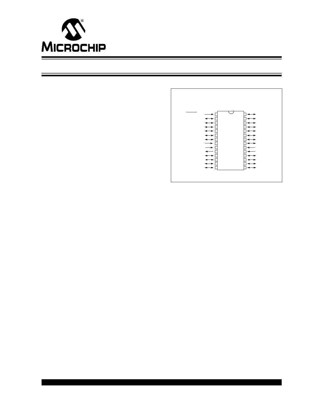
Pin Diagram
Peripheral Features:
• Timer0: 8-bit timer/counter with 8-bit prescaler
• Timer1: 16-bit timer/counter with prescaler,
can be incremented during sleep via external
crystal/clock
• Timer2: 8-bit timer/counter with 8-bit period
register, prescaler and postscaler
• Capture, Compare, PWM module
• Capture is 16-bit, max. resolution is 12.5 ns,
Compare is 16-bit, max. resolution is 200 ns,
PWM maximum resolution is 10-bit
• 8-bit multi-channel Analog-to-Digital converter
• Synchronous Serial Port (SSP) with Enhanced
SPI and I
2
C
P
IC16
C
72A
MCLR/V
PP
RA0/AN0
RA1/AN1
RA2/AN2
RA3/AN3/V
REF
RA4/T0CKI
RA5/SS/AN4
V
SS
OSC1/CLKIN
OSC2/CLKOUT
RC0/T1OSO/T1CKI
RC1/T1OSI
RC2/CCP1
RC3/SCK/SCL
RB7
RB6
RB5
RB4
RB3
RB2
RB1
RB0/INT
V
DD
V
SS
RC7
RC6
RC5/SDO
RC4/SDI/SDA
• 1
2
3
4
5
6
7
8
9
10
11
12
13
14
28
27
26
25
24
23
22
21
20
19
18
17
16
15
SDIP, SOIC, SSOP, Windowed CERDIP
PIC16C62B/72A
28-Pin 8-Bit CMOS Microcontrollers
PIC16C62B/72A
DS35008C-page 2
Preliminary
1998-2013 Microchip Technology Inc.
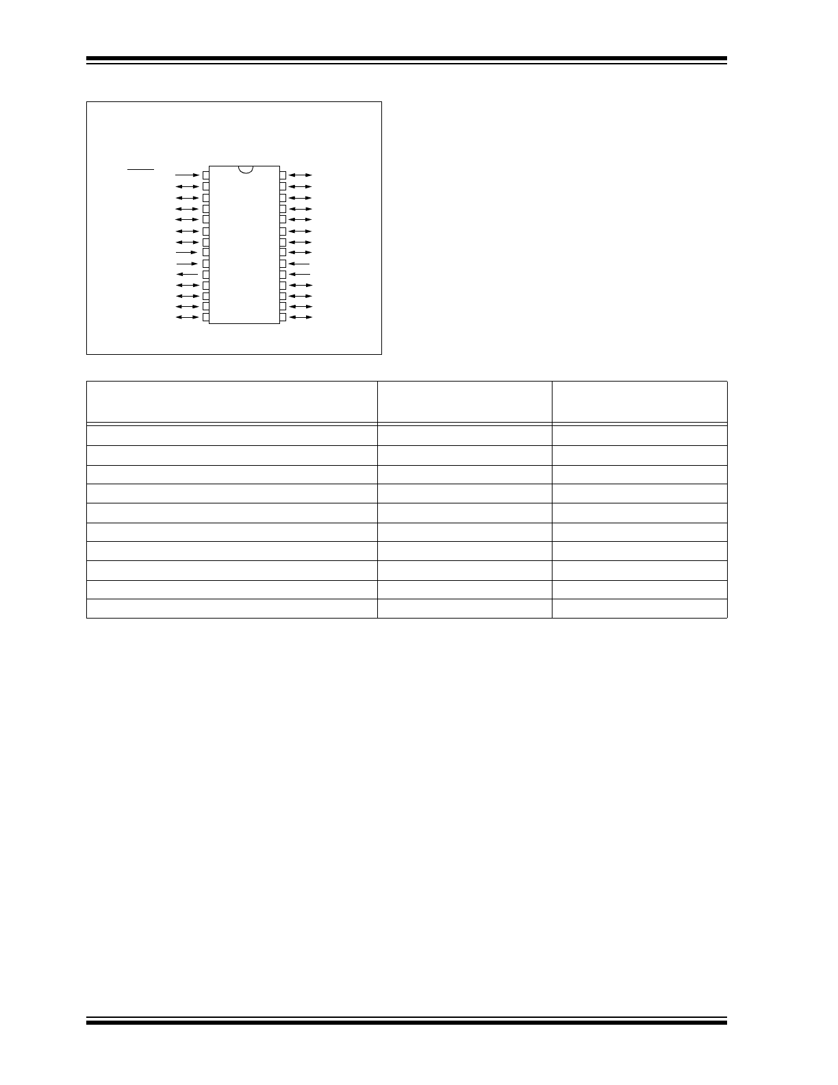
Pin Diagrams
P
IC16
C
62B
MCLR/V
PP
RA0
RA1
RA2
RA3
RA4/T0CKI
RA5/SS
V
SS
OSC1/CLKIN
OSC2/CLKOUT
RC0/T1OSO/T1CKI
RC1/T1OSI
RC2/CCP1
RC3/SCK/SCL
RB7
RB6
RB5
RB4
RB3
RB2
RB1
RB0/INT
V
DD
V
SS
RC7
RC6
RC5/SDO
RC4/SDI/SDA
• 1
2
3
4
5
6
7
8
9
10
11
12
13
14
28
27
26
25
24
23
22
21
20
19
18
17
16
15
SDIP, SOIC, SSOP, Windowed CERDIP
Key Features
PIC
®
Mid-Range Reference Manual (DS33023)
PIC16C62B
PIC16C72A
Operating Frequency
DC - 20 MHz
DC - 20 MHz
Resets (and Delays)
POR, BOR (PWRT, OST)
POR, BOR (PWRT, OST)
Program Memory (14-bit words)
2K
2K
Data Memory (bytes)
128
128
Interrupts
7
8
I/O Ports
Ports A,B,C
Ports A,B,C
Timers
3
3
Capture/Compare/PWM modules
1
1
Serial Communications
SSP
SSP
8-bit Analog-to-Digital Module
—
5 input channels

PIC16C62B/72A
1998-2013 Microchip Technology Inc.
Preliminary
DS35008C-page 3
Table of Contents
1.0
Device Overview .................................................................................................................................................... 5
2.0
Memory Organization ............................................................................................................................................. 7
3.0
I/O Ports ............................................................................................................................................................... 19
4.0
Timer0 Module ..................................................................................................................................................... 25
5.0
Timer1 Module ..................................................................................................................................................... 27
6.0
Timer2 Module ..................................................................................................................................................... 31
7.0
Capture/Compare/PWM (CCP) Module ............................................................................................................... 33
8.0
Synchronous Serial Port (SSP) Module ............................................................................................................... 39
9.0
Analog-to-Digital Converter (A/D) Module ............................................................................................................ 49
10.0 Special Features of the CPU................................................................................................................................ 55
11.0 Instruction Set Summary ...................................................................................................................................... 67
12.0 Development Support........................................................................................................................................... 75
13.0 Electrical Characteristics ...................................................................................................................................... 81
14.0 DC and AC Characteristics Graphs and Tables ................................................................................................. 103
15.0 Packaging Information........................................................................................................................................ 105
Appendix A: Revision History ................................................................................................................................... 111
Appendix B: Conversion Considerations .................................................................................................................. 111
Appendix C: Migration from Base-line to Mid-Range Devices .................................................................................. 112
Index ........................................................................................................................................................................... 113
On-Line Support.......................................................................................................................................................... 117
Reader Response ....................................................................................................................................................... 118
PIC16C62B/72A Product Identification System .......................................................................................................... 119
To Our Valued Customers
Most Current Data Sheet
To obtain the most up-to-date version of this data sheet, please register at our Worldwide Web site at:
http://www.microchip.com
You can determine the version of a data sheet by examining its literature number found on the bottom outside corner of any page.
The last character of the literature number is the version number. e.g., DS30000A is version A of document DS30000.
New Customer Notification System
Register on our web site (www.microchip.com/cn) to receive the most current information on our products.
Errata
An errata sheet may exist for current devices, describing minor operational differences (from the data sheet) and recommended
workarounds. As device/documentation issues become known to us, we will publish an errata sheet. The errata will specify the revi-
sion of silicon and revision of document to which it applies.
To determine if an errata sheet exists for a particular device, please check with one of the following:
• Microchip’s Worldwide Web site; http://www.microchip.com
• Your local Microchip sales office (see last page)
• The Microchip Corporate Literature Center; U.S. FAX: (480) 786-7277
When contacting a sales office or the literature center, please specify which device, revision of silicon and data sheet (include liter-
ature number) you are using.
Corrections to this Data Sheet
We constantly strive to improve the quality of all our products and documentation. We have spent a great deal of time to ensure that
this document is correct. However, we realize that we may have missed a few things. If you find any information that is missing or
appears in error, please:
• Fill out and mail in the reader response form in the back of this data sheet.
• E-mail us at webmaster@microchip.com.
We appreciate your assistance in making this a better document.

PIC16C62B/72A
DS35008C-page 4
Preliminary
1998-2013 Microchip Technology Inc.
NOTES:
PIC16C62B/72A
1998-2013 Microchip Technology Inc.
Preliminary
DS35008C-page 5
1.0
DEVICE OVERVIEW
This document contains device-specific information.
Additional information may be found in the PIC
®
MCU
Mid-Range Reference Manual, (DS33023), which may
be obtained from your local Microchip Sales Represen-
tative or downloaded from the Microchip website. The
Reference Manual should be considered a comple-
mentary document to this data sheet, and is highly rec-
ommended reading for a better understanding of the
device architecture and operation of the peripheral
modules.
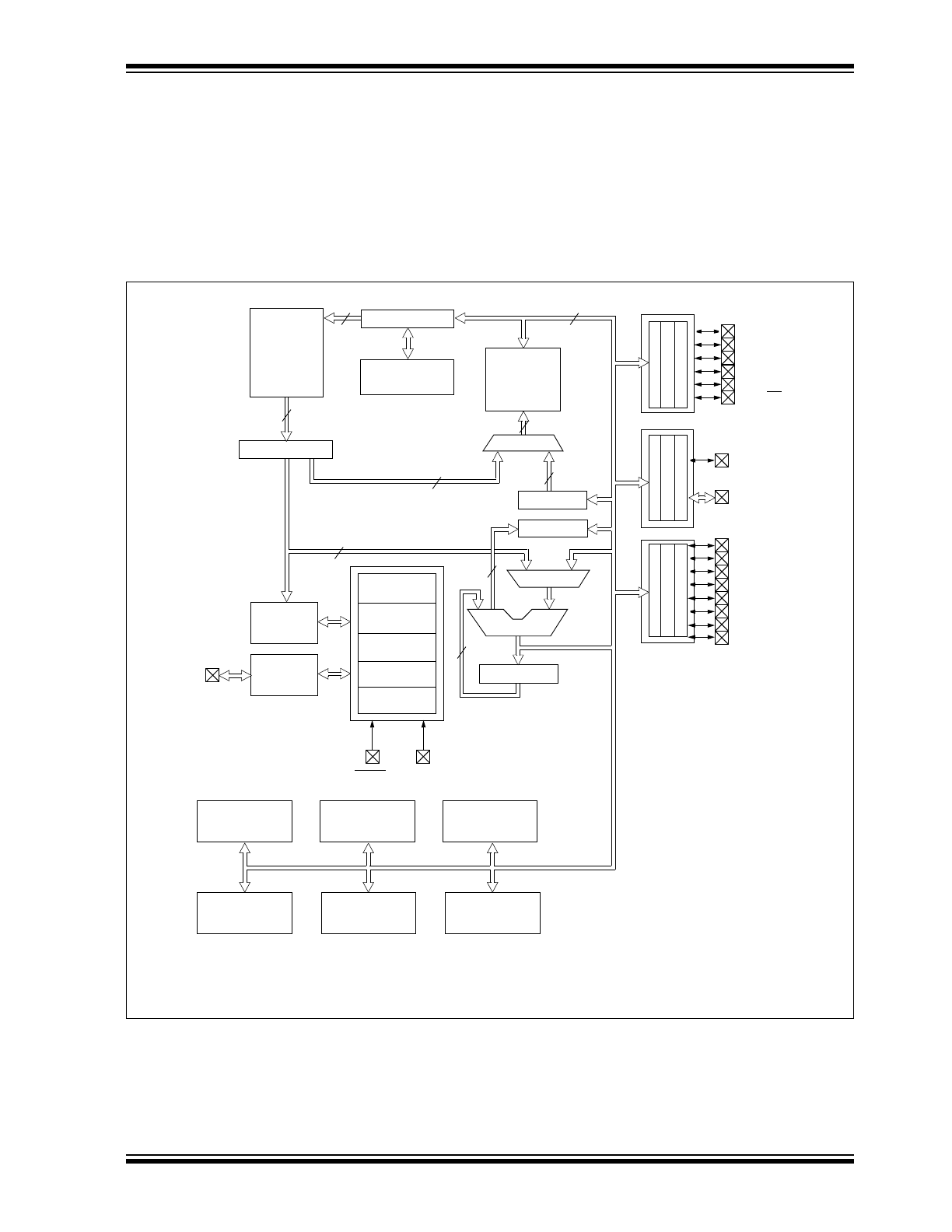
There are two devices (PIC16C62B, PIC16C72A) cov-
ered by this datasheet. The PIC16C62B does not have
the A/D module implemented.
Figure 1-1 is the block diagram for both devices. The
pinouts are listed in Table 1-1.
FIGURE 1-1:
PIC16C62B/PIC16C72A BLOCK DIAGRAM
EPROM
Program
Memory
13
Data Bus
8
14
Program
Bus
Instruction reg
Program Counter
8 Level Stack
(13-bit)
RAM
File
Registers
Direct Addr
7
RAM Addr
(1)
9
Addr MUX
Indirect
Addr
FSR reg
STATUS reg
MUX
ALU
W reg
Power-up
Timer
Oscillator
Start-up Timer
Power-on
Reset
Watchdog
Timer
Instruction
Decode &
Control
Timing
Generation
OSC1/CLKIN
OSC2/CLKOUT
MCLR
V
DD
, V
SS
PORTA
PORTB
PORTC
RB0/INT
RB7:RB1
RC0/T1OSO/T1CKI
RC1/T1OSI
RC2/CCP1
RC3/SCK/SCL
RC4/SDI/SDA
RC5/SDO
RC6
RC7
8
8
Brown-out
Reset
Note 1:
Higher order bits are from the STATUS register.
2: The A/D module is not available on the PIC16C62B.
CCP1
Synchronous
A/D
(2)
Timer0
Timer1
Timer2
Serial Port
RA4/T0CKI
RA5/SS/AN4
(2)
RA3/AN3/V
REF
(2)
RA2/AN2
(2)
RA1/AN1
(2)
RA0/AN0
(2)
8
3
2K x 14
128 x 8
PIC16C62B/72A
DS35008C-page 6
Preliminary
1998-2013 Microchip Technology Inc.
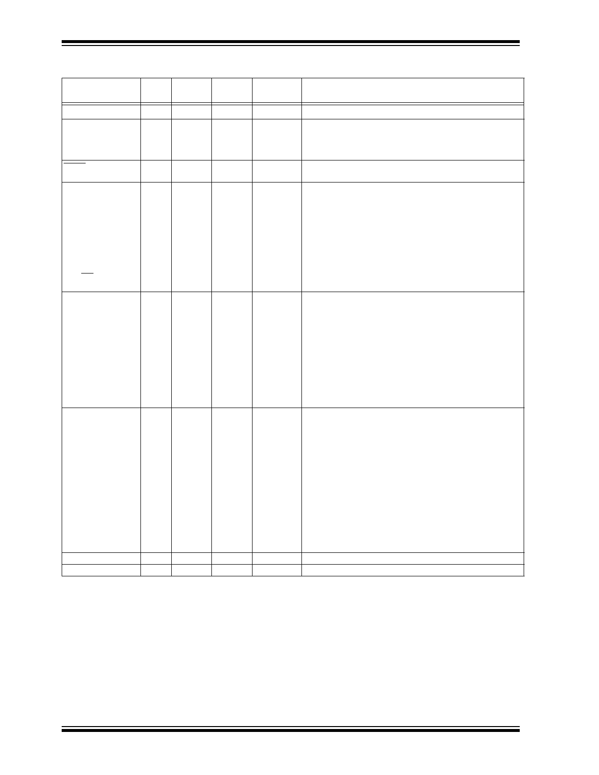
TABLE 1-1
PIC16C62B/PIC16C72A PINOUT DESCRIPTION
Pin Name
DIP
Pin#
SOIC
Pin#
I/O/P
Type
Buffer
Type
Description
OSC1/CLKIN
9
9
I
ST/CMOS
(3)
Oscillator crystal input/external clock source input.
OSC2/CLKOUT
10
10
O
—
Oscillator crystal output. Connects to crystal or resonator in
crystal oscillator mode. In RC mode, the OSC2 pin outputs
CLKOUT which has 1/4 the frequency of OSC1, and denotes
the instruction cycle rate.
MCLR/V
PP
1
1
I/P
ST
Master clear (reset) input or programming voltage input. This
pin is an active low reset to the device.
PORTA is a bi-directional I/O port.
RA0/AN0
(4)
2
2
I/O
TTL
RA0 can also be analog input 0
RA1/AN1
(4)
3
3
I/O
TTL
RA1 can also be analog input 1
RA2/AN2
(4)
4
4
I/O
TTL
RA2 can also be analog input 2
RA3/AN3/V
REF
(4)
5
5
I/O
TTL
RA3 can also be analog input 3 or analog reference voltage
RA4/T0CKI
6
6
I/O
ST
RA4 can also be the clock input to the Timer0 module.
Output is open drain type.
RA5/SS/AN4
(4)
7
7
I/O
TTL
RA5 can also be analog input 4 or the slave select for the
synchronous serial port.
PORTB is a bi-directional I/O port. PORTB can be software
programmed for internal weak pull-up on all inputs.
RB0/INT
21
21
I/O
TTL/ST
(1)
RB0 can also be the external interrupt pin.
RB1
22
22
I/O
TTL
RB2
23
23
I/O
TTL
RB3
24
24
I/O
TTL
RB4
25
25
I/O
TTL
Interrupt on change pin.
RB5
26
26
I/O
TTL
Interrupt on change pin.
RB6
27
27
I/O
TTL/ST
(2)
Interrupt on change pin. Serial programming clock.
RB7
28
28
I/O
TTL/ST
(2)
Interrupt on change pin. Serial programming data.
PORTC is a bi-directional I/O port.
RC0/T1OSO/T1CKI
11
11
I/O
ST
RC0 can also be the Timer1 oscillator output or Timer1
clock input.
RC1/T1OSI
12
12
I/O
ST
RC1 can also be the Timer1 oscillator input.
RC2/CCP1
13
13
I/O
ST
RC2 can also be the Capture1 input/Compare1 output/
PWM1 output.
RC3/SCK/SCL
14
14
I/O
ST
RC3 can also be the synchronous serial clock input/output
for both SPI and I
2
C modes.
RC4/SDI/SDA
15
15
I/O
ST
RC4 can also be the SPI Data In (SPI mode) or
data I/O (I
2
C mode).
RC5/SDO
16
16
I/O
ST
RC5 can also be the SPI Data Out (SPI mode).
RC6
17
17
I/O
ST
RC7
18
18
I/O
ST
V
SS
8, 19
8, 19
P
—
Ground reference for logic and I/O pins.
V
DD
20
20
P
—
Positive supply for logic and I/O pins.
Legend: I = input
O = output
I/O = input/output
P = power or program
— = Not used
TTL = TTL input
ST = Schmitt Trigger input
Note 1: This buffer is a Schmitt Trigger input when configured as the external interrupt.
2: This buffer is a Schmitt Trigger input when used in serial programming mode.
3: This buffer is a Schmitt Trigger input when configured in RC oscillator mode and a CMOS input otherwise.
4: The A/D module is not available on the PIC16C62B.
PIC16C62B/72A
1998-2013 Microchip Technology Inc.
Preliminary
DS35008C-page 7
2.0
MEMORY ORGANIZATION
There are two memory blocks in each of these micro-
controllers. Each block (Program Memory and Data
Memory) has its own bus, so that concurrent access
can occur.
Additional information on device memory may be found
in the PICmicro
Mid-Range Reference Manual,
(DS33023).
2.1
Program Memory Organization
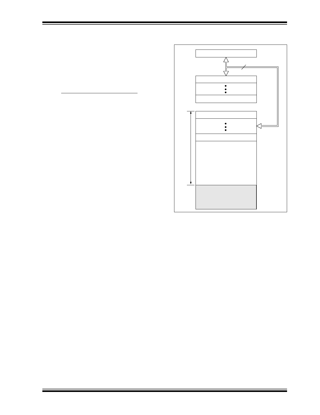
The PIC16C62B/72A devices have a 13-bit program
counter capable of addressing an 8K x 14 program
memory space. Each device has 2K x 14 words of pro-
gram memory. Accessing a location above 07FFh will
cause a wraparound.
The reset vector is at 0000h and the interrupt vector is
at 0004h.
FIGURE 2-1:
PROGRAM MEMORY MAP
AND STACK
PC<12:0>
13
0000h
0004h
0005h
07FFh
0800h
1FFFh
Stack Level 1
Stack Level 8
Reset Vector
Interrupt Vector
On-chip Program
Memory
CALL, RETURN
RETFIE, RETLW
Use
r Me
mo
ry
S
pac
e
PIC16C62B/72A
DS35008C-page 8
Preliminary
1998-2013 Microchip Technology Inc.
2.2
Data Memory Organization
The data memory is partitioned into multiple banks
which contain the General Purpose Registers and the
Special Function Registers. Bits RP1 and RP0 are the
bank select bits.
= 00
Bank0
= 01
Bank1
= 10
Bank2 (not implemented)
= 11
Bank3 (not implemented)
Each bank extends up to 7Fh (128 bytes). The lower
locations of each bank are reserved for the Special
Function Registers. Above the Special Function Regis-
ters are General Purpose Registers, implemented as
static RAM. All implemented banks contain Special
Function Registers. Some “high use” Special Function
Registers from one bank may be mirrored in another
bank for code reduction and quicker access.
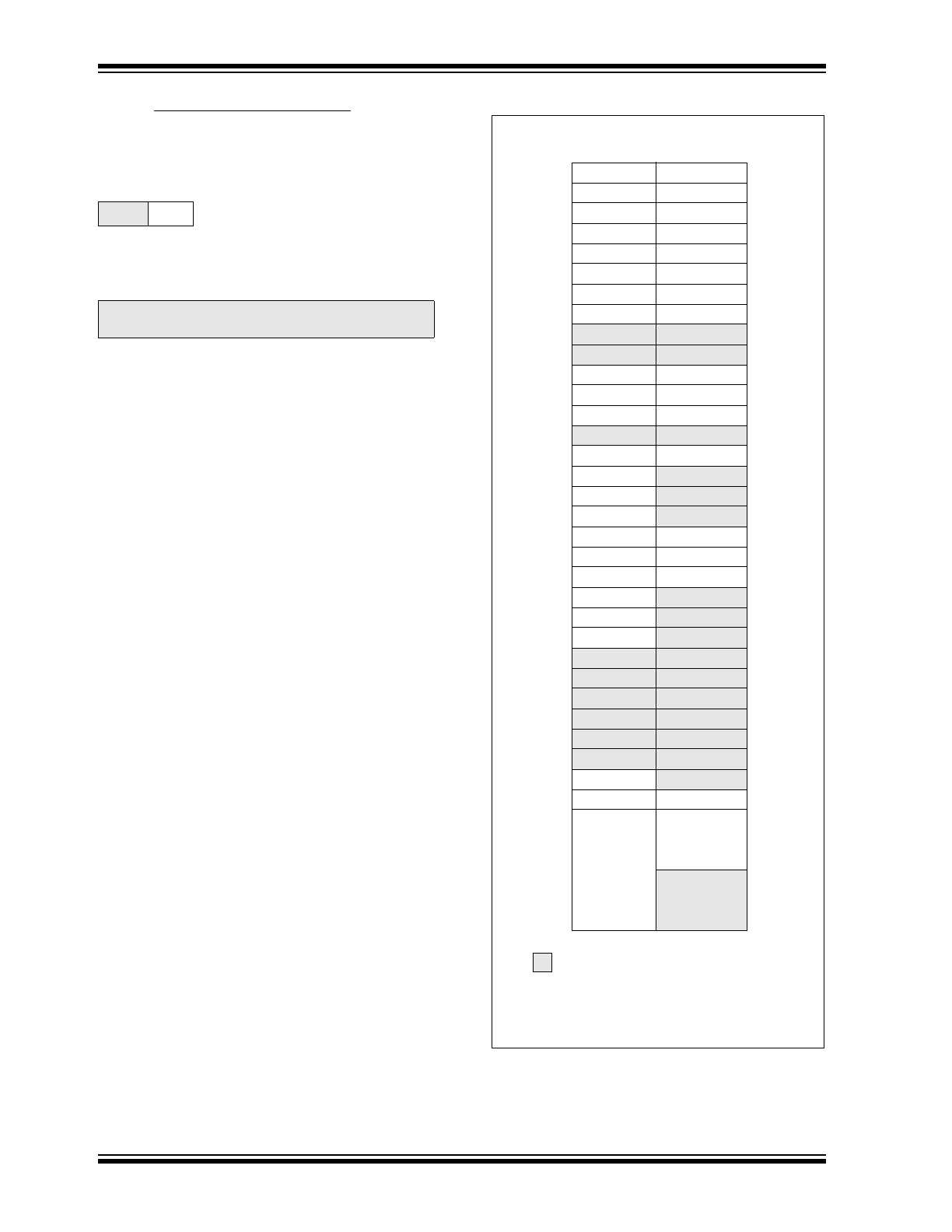
2.2.1
GENERAL PURPOSE REGISTER FILE
The register file can be accessed either directly, or indi-
rectly through the File Select Register FSR
(Section 2.5).
FIGURE 2-2:
REGISTER FILE MAP
RP1
(1)
RP0
(STATUS<6:5>)
Note 1: Maintain this bit clear to ensure upward compati-
bility with future products.
Unimplemented data memory locations,
read as '0'.
Note 1: Not a physical register.
2:
These registers are not implemented on the
PIC16C62B, read as '0'.
File
Address
File
Address
00h
INDF
(1)
INDF
(1)
80h
01h
TMR0
OPTION_REG 81h
02h
PCL
PCL
82h
03h
STATUS
STATUS
83h
04h
FSR
FSR
84h
05h
PORTA
TRISA
85h
06h
PORTB
TRISB
86h
07h
PORTC
TRISC
87h
08h
—
—
88h
09h
—
—
89h
0Ah
PCLATH
PCLATH
8Ah
0Bh
INTCON
INTCON
8Bh
0Ch
PIR1
PIE1
8Ch
0Dh
—
—
8Dh
0Eh
TMR1L
PCON
8Eh
0Fh
TMR1H
—
8Fh
10h
T1CON
—
90h
11h
TMR2
—
91h
12h
T2CON
PR2
92h
13h
SSPBUF
SSPADD
93h
14h
SSPCON
SSPSTAT
94h
15h
CCPR1L
—
95h
16h
CCPR1H
—
96h
17h
CCP1CON
—
97h
18h
—
—
98h
19h
—
—
99h
1Ah
—
—
9Ah
1Bh
—
—
9Bh
1Ch
—
—
9Ch
1Dh
—
—
9Dh
1Eh
ADRES
(2)
—
9Eh
1Fh
ADCON0
(2)
ADCON1
(2)
9Fh
20h
General
Purpose
Registers
General
Purpose
Registers
A0h
BFh
—
C0h
—
7Fh
—
FFh
Bank 0
Bank 1
PIC16C62B/72A
1998-2013 Microchip Technology Inc.
Preliminary
DS35008C-page 9
2.2.2
SPECIAL FUNCTION REGISTERS
The Special Function Registers are registers used by
the CPU and Peripheral Modules for controlling the
desired operation of the device. These registers are
implemented as static RAM. A list of these registers is
given in Table 2-1.
The Special Function Registers can be classified into
two sets; core (CPU) and peripheral. Those registers
associated with the core functions are described in
detail in this section. Those related to the operation of
the peripheral features are described in detail in the
peripheral feature section.
TABLE 2-1
SPECIAL FUNCTION REGISTER SUMMARY
Addr
Name
Bit 7
Bit 6
Bit 5
Bit 4
Bit 3
Bit 2
Bit 1
Bit 0
Value on:
POR,
BOR
Value on all
other resets
(4)
Bank 0
00h
INDF
(1)
Addressing this location uses contents of FSR to address data memory (not a physical register) 0000 0000 0000 0000
01h
TMR0
Timer0 module’s register
xxxx xxxx
uuuu uuuu
02h
PCL
(1)
Program Counter's (PC) Least Significant Byte
0000 0000
0000 0000
03h
STATUS
(1)
IRP
(5)
RP1
(5)
RP0
TO
PD
Z
DC
C
0001 1xxx
000q quuu
04h
FSR
(1)
Indirect data memory address pointer
xxxx xxxx
uuuu uuuu
05h
PORTA
(6,7)
—
—
PORTA Data Latch when written: PORTA pins when read
--0x 0000
--0u 0000
06h
PORTB
(6,7)
PORTB Data Latch when written: PORTB pins when read
xxxx xxxx
uuuu uuuu
07h
PORTC
(6,7)
PORTC Data Latch when written: PORTC pins when read
xxxx xxxx
uuuu uuuu
08h-09h
—
Unimplemented
—
—
0Ah
PCLATH
(1,2)
—
—
—
Write Buffer for the upper 5 bits of the Program Counter
---0 0000
---0 0000
0Bh
INTCON
(1)
GIE PEIE
T0IE
INTE
RBIE
T0IF
INTF
RBIF
0000 000x
0000 000u
0Ch
PIR1
—
ADIF
(3)
—
—
SSPIF
CCP1IF
TMR2IF
TMR1IF
-0-- 0000
-0-- 0000
0Dh
—
Unimplemented
—
—
0Eh
TMR1L
Holding register for the Least Significant Byte of the 16-bit TMR1 register
xxxx xxxx
uuuu uuuu
0Fh
TMR1H
Holding register for the Most Significant Byte of the 16-bit TMR1 register
xxxx xxxx
uuuu uuuu
10h
T1CON
—
—
T1CKPS1 T1CKPS0 T1OSCEN
T1SYNC
TMR1CS
TMR1ON
--00 0000
--uu uuuu
11h
TMR2
Timer2 module’s register
0000 0000
0000 0000
12h
T2CON
—
TOUTPS3 TOUTPS2 TOUTPS1 TOUTPS0
TMR2ON
T2CKPS1 T2CKPS0 -000 0000 -000 0000
13h
SSPBUF
Synchronous Serial Port Receive Buffer/Transmit Register
xxxx xxxx
uuuu uuuu
14h
SSPCON
WCOL
SSPOV
SSPEN
CKP
SSPM3
SSPM2
SSPM1
SSPM0
0000 0000
0000 0000
15h
CCPR1L
Capture/Compare/PWM Register1 (LSB)
xxxx xxxx
uuuu uuuu
16h
CCPR1H
Capture/Compare/PWM Register1 (MSB)
xxxx xxxx
uuuu uuuu
17h
CCP1CON
—
—
CCP1X
CCP1Y
CCP1M3
CCP1M2
CCP1M1
CCP1M0
--00 0000
--00 0000
18h-1Dh
—
Unimplemented
—
—
1Eh
ADRES
(3)
A/D Result Register
xxxx xxxx
uuuu uuuu
1Fh
ADCON0
(3)
ADCS1
ADCS0
CHS2
CHS1
CHS0
GO/DONE
—
ADON
0000 00-0
0000 00-0
Legend: x = unknown, u = unchanged, q = value depends on condition, - = unimplemented, read as '0',
Shaded locations are unimplemented, read as '0'.
Note 1: These registers can be addressed from either bank.
2:
The upper byte of the program counter is not directly accessible. PCLATH is a holding register for PC<12:8> whose contents
are transferred to the upper byte of the program counter.
3:
A/D not implemented on the PIC16C62B, maintain as ’0’.
4:
Other (non power-up) resets include: external reset through MCLR and the Watchdog Timer Reset.
5:
The IRP and RP1 bits are reserved. Always maintain these bits clear.
6:
On any device reset, these pins are configured as inputs.
7:
This is the value that will be in the port output latch.
PIC16C62B/72A
DS35008C-page 10
Preliminary
1998-2013 Microchip Technology Inc.
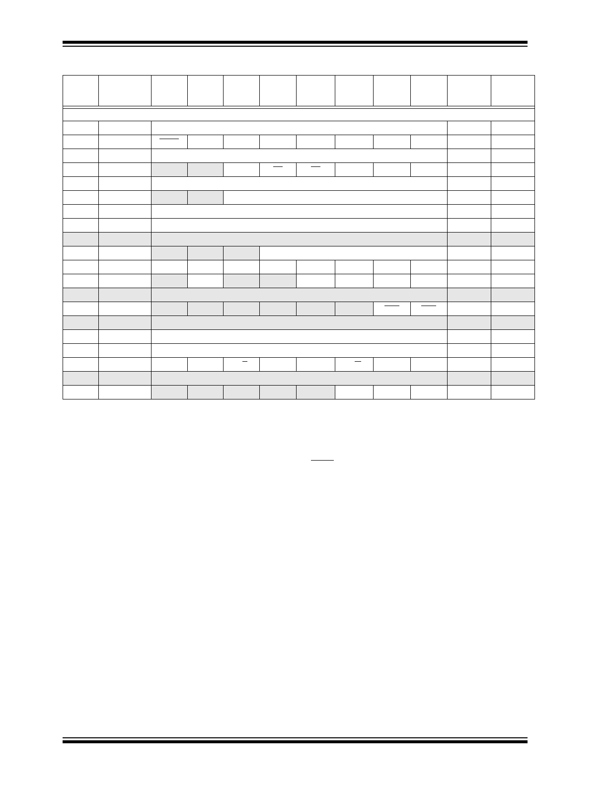
Bank 1
80h
INDF
(1)
Addressing this location uses contents of FSR to address data memory (not a physical register) 0000 0000 0000 0000
81h
OPTION_REG
RBPU
INTEDG
T0CS
T0SE
PSA
PS2
PS1
PS0
1111 1111
1111 1111
82h
PCL
(1)
Program Counter's (PC) Least Significant Byte
0000 0000
0000 0000
83h
STATUS
(1)
IRP
(5)
RP1
(5)
RP0
TO
PD
Z
DC
C
0001 1xxx
000q quuu
84h
FSR
(1)
Indirect data memory address pointer
xxxx xxxx
uuuu uuuu
85h
TRISA
—
—
PORTA Data Direction Register
--11 1111
--11 1111
86h
TRISB
PORTB Data Direction Register
1111 1111
1111 1111
87h
TRISC
PORTC Data Direction Register
1111 1111
1111 1111
88h-89h
—
Unimplemented
—
—
8Ah
PCLATH
(1,2)
—
—
—
Write Buffer for the upper 5 bits of the Program Counter
---0 0000
---0 0000
8Bh
INTCON
(1)
GIE
PEIE
T0IE
INTE
RBIE
T0IF
INTF
RBIF
0000 000x
0000 000u
8Ch
PIE1
—
ADIE
(3)
—
—
SSPIE
CCP1IE
TMR2IE
TMR1IE
-0-- 0000
-0-- 0000
8Dh
—
Unimplemented
—
—
8Eh
PCON
—
—
—
—
—
—
POR
BOR
---- --uu
8Fh-91h
—
Unimplemented
—
—
92h
PR2
Timer2 Period Register
1111 1111
1111 1111
93h
SSPADD
Synchronous Serial Port (I
2
C mode) Address Register
0000 0000
0000 0000
94h
SSPSTAT
SMP
CKE
D/A
P
S
R/W
UA
BF
0000 0000
0000 0000
95h-9Eh
—
Unimplemented
—
—
9Fh
ADCON1
(3)
—
—
—
—
—
PCFG2
PCFG1
PCFG0
---- -000 ---- -000
Legend: x = unknown, u = unchanged, q = value depends on condition, - = unimplemented, read as '0',
Shaded locations are unimplemented, read as '0'.
Note 1: These registers can be addressed from either bank.
2: The upper byte of the program counter is not directly accessible. PCLATH is a holding register for PC<12:8> whose contents
are transferred to the upper byte of the program counter.
3: A/D not implemented on the PIC16C62B, maintain as ’0’.
4: Other (non power-up) resets include: external reset through MCLR and the Watchdog Timer Reset.
5: The IRP and RP1 bits are reserved. Always maintain these bits clear.
6: On any device reset, these pins are configured as inputs.
7: This is the value that will be in the port output latch.
TABLE 2-1
SPECIAL FUNCTION REGISTER SUMMARY (Cont.’d)
Addr
Name
Bit 7
Bit 6
Bit 5
Bit 4
Bit 3
Bit 2
Bit 1
Bit 0
Value on:
POR,
BOR
Value on all
other resets
(4)