
Appendix A – ATtiny25/V Specification at 105°C
This document contains information specific to devices operating at temperatures up
to 105°C. Only deviations are covered in this appendix, all other information can be
found in the complete datasheet. The complete datasheet can be found at
www.atmel.com.
8-bit
Microcontroller
with 2K Bytes
In-System
Programmable
Flash
ATtiny25/V
Appendix A
Rev. 2586N–Appendix A–AVR–08/11
2
2586N–Appendix A–AVR–08/11
ATtiny25
1.
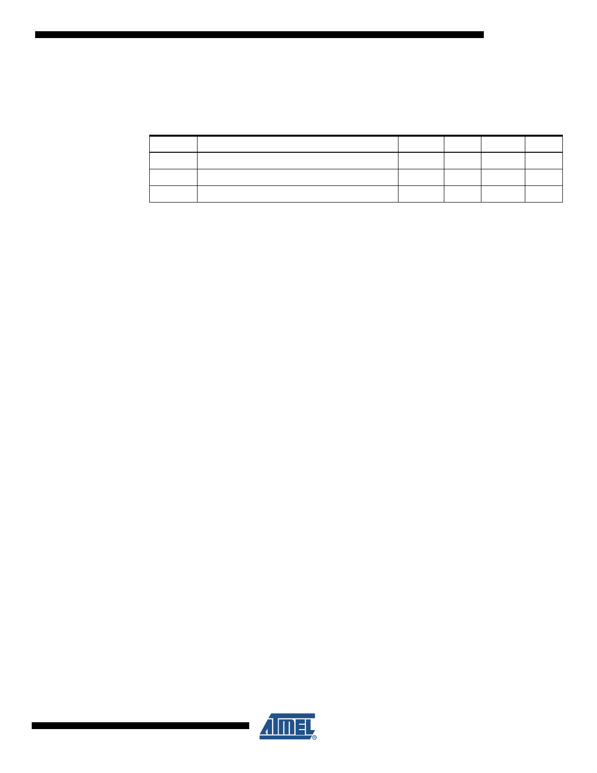
Electrical Characteristics
1.1
Absolute Maximum Ratings*
1.2
DC Characteristics
Operating Temperature.................................. -55
°
C to +125
°
C
*NOTICE:
Stresses beyond those listed under “Absolute
Maximum Ratings” may cause permanent dam-
age to the device. This is a stress rating only and
functional operation of the device at these or
other conditions beyond those indicated in the
operational sections of this specification is not
implied. Exposure to absolute maximum rating
conditions for extended periods may affect
device reliability.
Storage Temperature ..................................... -65°C to +150°C
Voltage on any Pin except RESET
with respect to Ground ................................-0.5V to V
CC
+0.5V
Voltage on RESET with respect to Ground......-0.5V to +13.0V
Maximum Operating Voltage ............................................ 6.0V
DC Current per I/O Pin ............................................... 40.0 mA
DC Current
V
CC
and GND Pins................................ 200.0 mA
Table 1-1.
DC Characteristics. T
A
= -40
°
C to +105
°
C
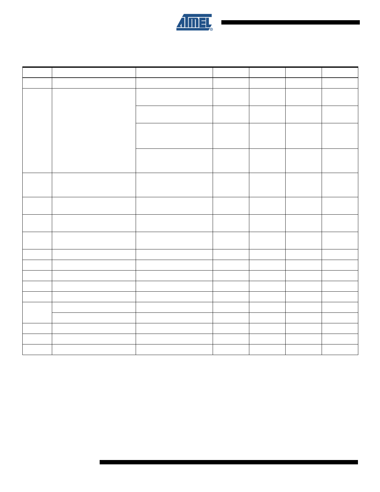
Symbol
Parameter
Condition
Min.
Typ.
(1)
Max.
Units
V
IL
Input Low-voltage, except
XTAL1 and RESET pin
V
CC
= 1.8V - 2.4V
V
CC
= 2.4V - 5.5V
-0.5
-0.5
0.2V
CC
(3)
0.3V
CC
(3)
V
V
V
IH
Input High-voltage, except
XTAL1 and RESET pin
V
CC
= 1.8V - 2.4V
V
CC
= 2.4V - 5.5V
0.7V
CC
(2)
0.6V
CC
(2)
V
CC
+0.5
V
CC
+0.5
V
V
V
IL1
Input Low-voltage, XTAL1 pin,
External Clock Selected
V
CC
= 1.8V - 5.5V
-0.5
0.1V
CC
(3)
V
V
IH1
Input High-voltage, XTAL1 pin,
External Clock Selected
V
CC
= 1.8V - 2.4V
V
CC
= 2.4V - 5.5V
0.8V
CC
(2)
0.7V
CC
(2)
V
CC
+0.5
V
CC
+0.5
V
V
V
IL2
Input Low-voltage,
RESET pin
V
CC
= 1.8V - 5.5V
-0.5
0.2V
CC
(3)
V
V
V
IH2
Input High-voltage,
RESET pin
V
CC
= 1.8V - 5.5V
0.9V
CC
(2)
V
CC
+0.5
V
V
IL3
Input Low-voltage,
RESET pin as I/O
V
CC
= 1.8V - 2.4V
V
CC
= 2.4V - 5.5V
-0.5
-0.5
0.2V
CC
(3)
0.3V
CC
(3)
V
V
V
IH3
Input High-voltage,
RESET pin as I/O
V
CC
= 1.8V - 2.4V
V
CC
= 2.4V - 5.5V
0.7V
CC
(2)
0.6V
CC
(2)
V
CC
+0.5
V
CC
+0.5
V
V
V
OL
Output Low-voltage
(4)
,
Port B (except RESET)
(6)
I
OL
= 10 mA, V
CC
= 5V
I
OL
= 5 mA, V
CC
= 3V
0.6
0.5
V
V
V
OH
Output High-voltage
(5)
,
Port B (except RESET)
(6)
I
OH
= -10 mA, V
CC
= 5V
I
OH
= -5 mA, V
CC
= 3V
4.3
2.5
V
V
I
IL
Input Leakage
Current I/O Pin
V
CC
= 5.5V, pin low
(absolute value)
< 0.05
1
µA
I
IH
Input Leakage
Current I/O Pin
V
CC
= 5.5V, pin high
(absolute value)
< 0.05
1
µA
3
2586N–Appendix A–AVR–08/11
ATtiny25
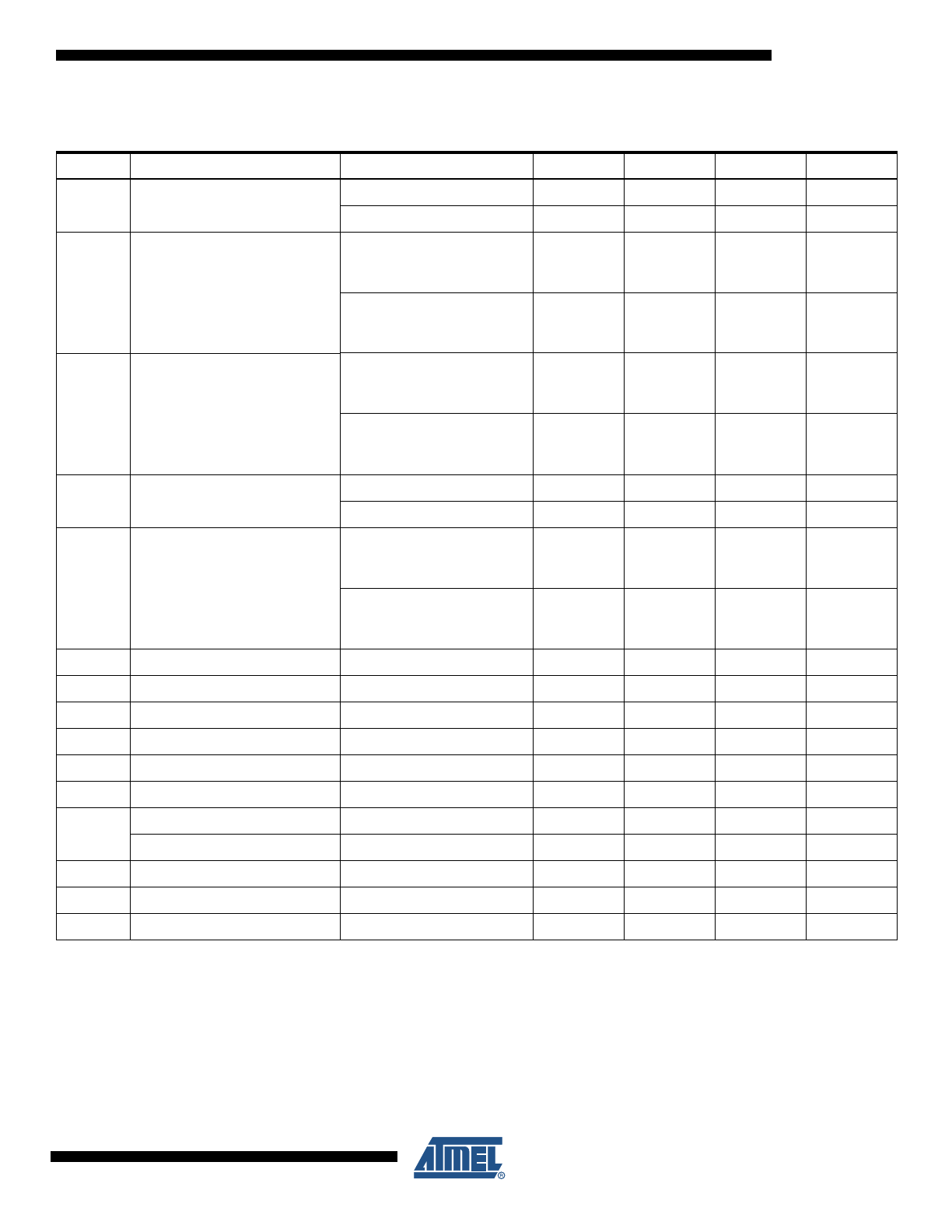
Notes:
1. Typical values at 25
°
C.
2. “Min” means the lowest value where the pin is guaranteed to be read as high.
3. “Max” means the highest value where the pin is guaranteed to be read as low.
4. Although each I/O port can sink more than the test conditions (10 mA at V
CC
= 5V, 5 mA at V
CC
= 3V) under steady state
conditions (non-transient), the following must be observed:
1] The sum of all IOL, for all ports, should not exceed 60 mA.
If IOL exceeds the test condition, VOL may exceed the related specification. Pins are not guaranteed to sink current greater
than the listed test condition.
5. Although each I/O port can source more than the test conditions (10 mA at V
CC
= 5V, 5 mA at V
CC
= 3V) under steady state
conditions (non-transient), the following must be observed:
1] The sum of all IOH, for all ports, should not exceed 60 mA.
If IOH exceeds the test condition, VOH may exceed the related specification. Pins are not guaranteed to source current
greater than the listed test condition.
6. The RESET pin must tolerate high voltages when entering and operating in programming modes and, as a consequence,
has a weak drive strength as compared to regular I/O pins.
7. Values are with external clock using methods described in
“Minimizing Power Consumption” on page 37
. Power Reduction is
enabled (PRR = 0xFF) and there is no I/O drive.
8. Brown-Out Detection (BOD) disabled.
R
RST
Reset Pull-up Resistor
V
CC
= 5.5V, input low
30
60
k
Ω
R
pu
I/O Pin Pull-up Resistor
V
CC
= 5.5V, input low
20
50
k
Ω
I
CC
Power Supply Current
(7)
Active 1MHz, V
CC
= 2V
0.3
0.55
mA
Active 4MHz, V
CC
= 3V
1.5
2.5
mA
Active 8MHz, V
CC
= 5V
5
8
mA
Idle 1MHz, V
CC
= 2V
0.1
0.2
mA
Idle 4MHz, V
CC
= 3V
0.35
0.6
mA
Idle 8MHz, V
CC
= 5V
1.2
2
mA
Power-down mode
(8)
WDT enabled, V
CC
= 3V
4
20
µA
WDT disabled, V
CC
= 3V
0.2
10
µA
Table 1-1.
DC Characteristics. T
A
= -40
°
C to +105
°
C (Continued)
Symbol
Parameter
Condition
Min.
Typ.
(1)
Max.
Units
4
2586N–Appendix A–AVR–08/11
ATtiny25
1.3
Clock Characteristics
1.3.1
Calibrated Internal RC Oscillator Accuracy
It is possible to manually calibrate the internal oscillator to be more accurate than default factory
calibration. Please note that the oscillator frequency depends on temperature and voltage. Volt-
age and temperature characteristics can be found in
Figure 2-36 on page 28
and
Figure 2-37 on
page 28
.
Notes:
1. Accuracy of oscillator frequency at calibration point (fixed temperature and fixed voltage).
2. ATtiny25/V, only: 6.4 MHz in ATtiny15 Compatibility Mode.
3. Voltage range for ATtiny25V.
4. Voltage range for ATtiny25.
1.4
System and Reset Characteristics
Note:
1. Values are guidelines only.
Table 1-2.
Calibration Accuracy of Internal RC Oscillator
Calibration
Method
Target Frequency
V
CC
Temperature
Accuracy at given Voltage
& Temperature
(1)
Factory
Calibration
8.0 MHz
(2)
3V
25
°
C
±10%
User
Calibration
Fixed frequency within:
6 – 8 MHz
Fixed voltage within:
1.8V - 5.5V
(3)
2.7V - 5.5V
(4)
Fixed temperature
within:
-40
°
C to +105
°
C
±1%
Table 1-3.
Reset, Brown-out and Internal Voltage Characteristics
Symbol
Parameter
Condition
Min
(1)
Typ
(1)
Max
(1)
Units
V
RST
RESET Pin Threshold Voltage
V
CC
= 3V
0.2 V
CC
0.9 V
CC
V
t
RST
Minimum pulse width on
RESET Pin
V
CC
= 3V
2.5
µs
V
HYST
Brown-out Detector Hysteresis
50
mV
t
BOD
Min Pulse Width on
Brown-out Reset
2
µs
V
BG
Bandgap reference
voltage
V
CC
= 5.5V
T
A
= 25°C
1.0
1.1
1.2
V
t
BG
Bandgap reference
start-up time
V
CC
= 2.7V
T
A
= 25°C
40
70
µs
I
BG
Bandgap reference
current consumption
V
CC
= 2.7V
T
A
= 25°C
15
µA
5
2586N–Appendix A–AVR–08/11
ATtiny25
1.4.1
Enhanced Power-On Reset
The table below describes the characteristics of the power-on reset.
Note:
1. Values are guidelines, only
2. Threshold where device is released from reset when voltage is rising
3. The Power-on Reset will not work unless the supply voltage has been below V
POT
(falling)
Table 1-4.
Characteristics of Enhanced Power-On Reset. T
A
= -40
°
C to +105
°
C
Symbol
Parameter
Min
(1)
Typ
(1)
Max
(1)
Units
V
POR
Release threshold of power-on reset
(2)
1.1
1.4
1.7
V
V
POA
Activation threshold of power-on reset
(3)
0.6
1.3
1.7
V
SR
ON
Power-On Slope Rate
0.01
V/ms
6
2586N–Appendix A–AVR–08/11
ATtiny25
1.5
ADC Characteristics – Preliminary
Note:
1. Values are guidelines only.
Table 1-5.
ADC Characteristics, Single Ended Channels. T
A
= -40
°
C to +105
°
C
Symbol
Parameter
Condition
Min
Typ
Max
Units
Resolution
10
Bits
Absolute accuracy
(Including INL, DNL, and
Quantization, Gain and
Offset errors)
V
REF
= 4V, V
CC
= 4V,
ADC clock = 200 kHz
2
LSB
V
REF
= 4V, V
CC
= 4V,
ADC clock = 1 MHz
3
LSB
V
REF
= 4V, V
CC
= 4V,
ADC clock = 200 kHz
Noise Reduction Mode
1.5
LSB
V
REF
= 4V, V
CC
= 4V,
ADC clock = 1 MHz
Noise Reduction Mode
2.5
LSB
Integral Non-linearity (INL)
(Accuracy after offset and gain
calibration)
V
REF
= 4V, V
CC
= 4V,
ADC clock = 200 kHz
1
LSB
Differential Non-linearity (DNL)
V
REF
= 4V, V
CC
= 4V,
ADC clock = 200 kHz
0.5
LSB
Gain Error
V
REF
= 4V, V
CC
= 4V,
ADC clock = 200 kHz
2.5
LSB
Offset Error
V
REF
= 4V, V
CC
= 4V,
ADC clock = 200 kHz
1.5
LSB
Conversion Time
Free Running Conversion
14
280
µs
Clock Frequency
50
1000
kHz
V
IN
Input Voltage
GND
V
REF
V
Input Bandwidth
38.4
kHz
AREF
External Reference Voltage
2.0
V
CC
V
V
INT
Internal Voltage Reference
1.0
1.1
1.2
V
Internal 2.56V Reference
(1)
V
CC
> 3.0V
2.3
2.56
2.8
V
R
REF
32
k
Ω
R
AIN
Analog Input Resistance
100
M
Ω
ADC Output
0
1023
LSB
7
2586N–Appendix A–AVR–08/11
ATtiny25
Note:
1. Values are guidelines only.
Table 1-6.
ADC Characteristics, Differential Channels (Unipolar Mode). T
A
= -40
°
C to +105
°
C
Symbol
Parameter
Condition
Min
Typ
Max
Units
Resolution
Gain = 1x
10
Bits
Gain = 20x
10
Bits
Absolute accuracy
(Including INL, DNL, and
Quantization, Gain and Offset
Errors)
Gain = 1x
V
REF
= 4V, V
CC
= 5V
ADC clock = 50 - 200 kHz
10.0
LSB
Gain = 20x
V
REF
= 4V, V
CC
= 5V
ADC clock = 50 - 200 kHz
20.0
LSB
Integral Non-Linearity (INL)
(Accuracy after Offset and
Gain Calibration)
Gain = 1x
V
REF
= 4V, V
CC
= 5V
ADC clock = 50 - 200 kHz
4.0
LSB
Gain = 20x
V
REF
= 4V, V
CC
= 5V
ADC clock = 50 - 200 kHz
10.0
LSB
Gain Error
Gain = 1x
10.0
LSB
Gain = 20x
15.0
LSB
Offset Error
Gain = 1x
V
REF
= 4V, V
CC
= 5V
ADC clock = 50 - 200 kHz
3.0
LSB
Gain = 20x
V
REF
= 4V, V
CC
= 5V
ADC clock = 50 - 200 kHz
4.0
LSB
Conversion Time
Free Running Conversion
70
280
µs
Clock Frequency
50
200
kHz
V
IN
Input Voltage
GND
V
CC
V
V
DIFF
Input Differential Voltage
V
REF
/Gain
V
Input Bandwidth
4
kHz
AREF
External Reference Voltage
2.0
V
CC
- 1.0
V
V
INT
Internal Voltage Reference
1.0
1.1
1.2
V
Internal 2.56V Reference
(1)
V
CC
> 3.0V
2.3
2.56
2.8
V
R
REF
Reference Input Resistance
32
k
Ω
R
AIN
Analog Input Resistance
100
M
Ω
ADC Conversion Output
0
1023
LSB
8
2586N–Appendix A–AVR–08/11
ATtiny25
Note:
1. Values are guidelines only.
Table 1-7.
ADC Characteristics, Differential Channels (Bipolar Mode). T
A
= -40
°
C to +105
°
C
Symbol
Parameter
Condition
Min
Typ
Max
Units
Resolution
Gain = 1x
10
Bits
Gain = 20x
10
Bits
Absolute accuracy
(Including INL, DNL, and
Quantization, Gain and Offset
Errors)
Gain = 1x
V
REF
= 4V, V
CC
= 5V
ADC clock = 50 - 200 kHz
8.0
LSB
Gain = 20x
V
REF
= 4V, V
CC
= 5V
ADC clock = 50 - 200 kHz
8.0
LSB
Integral Non-Linearity (INL)
(Accuracy after Offset and
Gain Calibration)
Gain = 1x
V
REF
= 4V, V
CC
= 5V
ADC clock = 50 - 200 kHz
4.0
LSB
Gain = 20x
V
REF
= 4V, V
CC
= 5V
ADC clock = 50 - 200 kHz
5.0
LSB
Gain Error
Gain = 1x
4.0
LSB
Gain = 20x
5.0
LSB
Offset Error
Gain = 1x
V
REF
= 4V, V
CC
= 5V
ADC clock = 50 - 200 kHz
3.0
LSB
Gain = 20x
V
REF
= 4V, V
CC
= 5V
ADC clock = 50 - 200 kHz
4.0
LSB
Conversion Time
Free Running Conversion
70
280
µs
Clock Frequency
50
200
kHz
V
IN
Input Voltage
GND
V
CC
V
V
DIFF
Input Differential Voltage
V
REF
/Gain
V
Input Bandwidth
4
kHz
AREF
External Reference Voltage
2.0
V
CC
- 1.0
V
V
INT
Internal Voltage Reference
1.0
1.1
1.2
V
Internal 2.56V Reference
(1)
V
CC
> 3.0V
2.3
2.56
2.8
V
R
REF
Reference Input Resistance
32
k
Ω
R
AIN
Analog Input Resistance
100
M
Ω
ADC Conversion Output
-512
511
LSB
9
2586N–Appendix A–AVR–08/11
ATtiny25
1.6
Serial Programming Characteristics
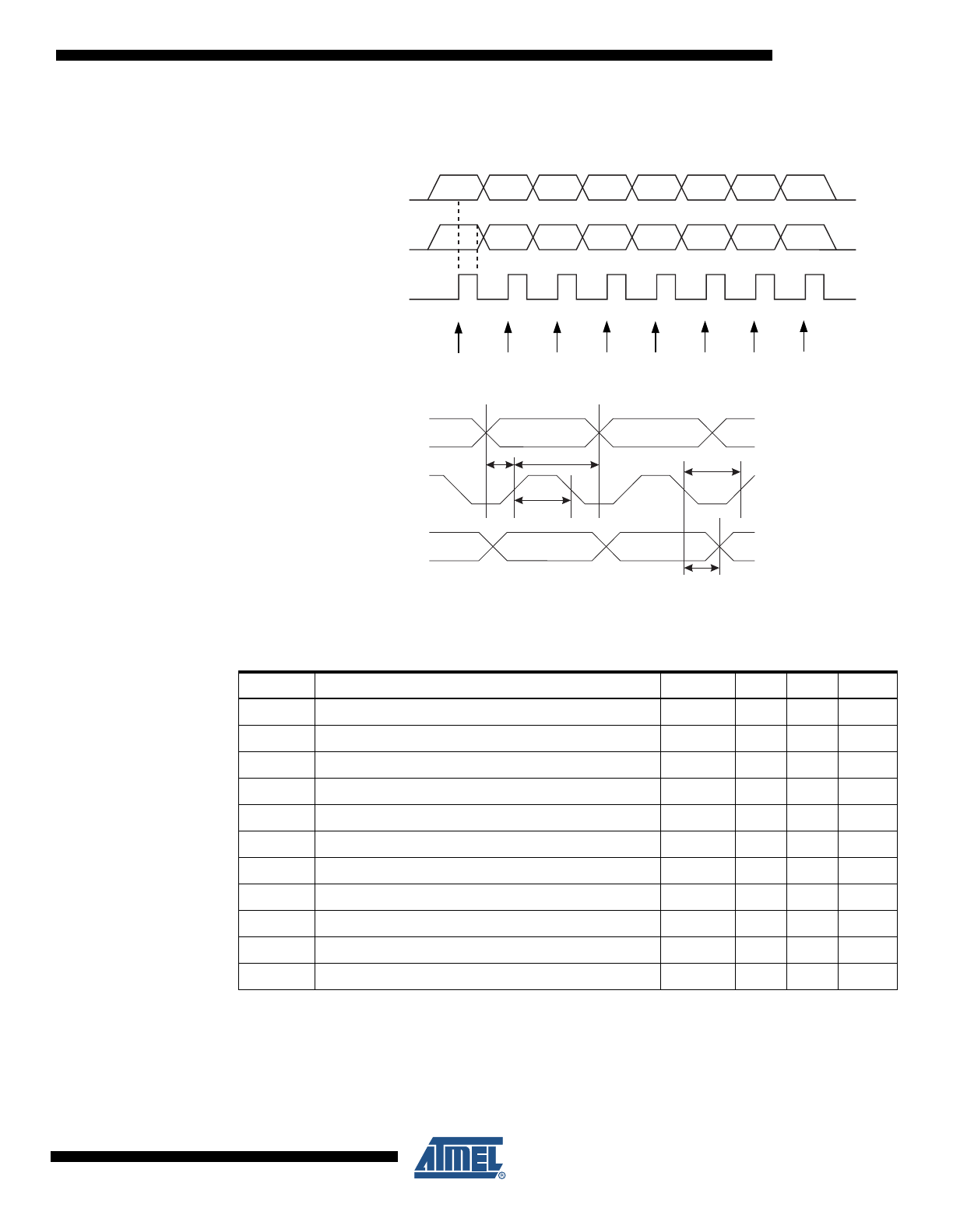
Figure 1-1.
Serial Programming Waveforms
Figure 1-2.
Serial Programming Timing
Note:
1. 2 t
CLCL
for f
ck
< 12 MHz, 3 t
CLCL
for f
ck
>= 12 MHz
Table 1-8.
Serial Programming Characteristics, T
A
= -40
°
C to +105
°
C, V
CC
= 1.8 - 5.5V
(Unless Otherwise Noted)
Symbol
Parameter
Min
Typ
Max
Units
1/t
CLCL
Oscillator Frequency (V
CC
= 1.8 - 5.5V)
0
4
MHz
t
CLCL
Oscillator Period (V
CC
= 1.8 - 5.5V)
250
ns
1/t
CLCL
Oscillator Frequency (V
CC
= 2.7 - 5.5V)
0
10
MHz
t
CLCL
Oscillator Period (V
CC
= 2.7 - 5.5V)
100
ns
1/t
CLCL
Oscillator Frequency (V
CC
= 4.5V - 5.5V)
0
20
MHz
t
CLCL
Oscillator Period (V
CC
= 4.5V - 5.5V)
50
ns
t
SHSL
SCK Pulse Width High
2 t
CLCL*
ns
t
SLSH
SCK Pulse Width Low
2 t
CLCL*
ns
t
OVSH
MOSI Setup to SCK High
t
CLCL
ns
t
SHOX
MOSI Hold after SCK High
2 t
CLCL
ns
t
SLIV
SCK Low to MISO Valid
100
ns
MSB
MSB
LSB
LSB
SERIAL CLOCK INPUT
(SCK)
SERIAL DATA INPUT
(MOSI)
(MISO)
SAMPLE
SERIAL DATA OUTPUT
MOSI
MISO
SCK
t
OVSH
t
SHSL
t
SLSH
t
SHOX
t
SLIV
10
2586N–Appendix A–AVR–08/11
ATtiny25
2.
Typical Characteristics
The data contained in this section is largely based on simulations and characterization of similar
devices in the same process and design methods. Thus, the data should be treated as indica-
tions of how the part will behave.
The following charts show typical behavior. These figures are not tested during manufacturing.
All current consumption measurements are performed with all I/O pins configured as inputs and
with internal pull-ups enabled. A sine wave generator with rail-to-rail output is used as clock
source.
The power consumption in Power-down mode is independent of clock selection.
The current consumption is a function of several factors such as: operating voltage, operating
frequency, loading of I/O pins, switching rate of I/O pins, code executed and ambient tempera-
ture. The dominating factors are operating voltage and frequency.
The current drawn from capacitive loaded pins may be estimated (for one pin) as C
L
*
V
CC
*f where
C
L
= load capacitance, V
CC
= operating voltage and f = average switching frequency of I/O pin.
The parts are characterized at frequencies higher than test limits. Parts are not guaranteed to
function properly at frequencies higher than the ordering code indicates.
The difference between current consumption in Power-down mode with Watchdog Timer
enabled and Power-down mode with Watchdog Timer disabled represents the differential cur-
rent drawn by the Watchdog Timer.
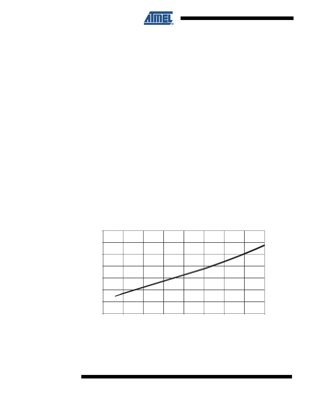
2.1
Active Supply Current
Figure 2-1.
Active Supply Current vs. V
CC
(Internal RC oscillator, 8 MHz)
ACTIVE SUPPLY CURRENT vs. V
CC
INTERNAL RC OSCILLATOR, 8 MHz
0
1
2
3
4
5
6
7
1,5
2
2,5
3
3,5
4
4,5
5
5,5
V
CC
(V)
I
CC
(mA)
25 °C
85 °C
105 °C
-40 °C