

Features
•
High-performance, Low-power Atmel
®
AVR
®
8-bit Microcontroller
•
Advanced RISC Architecture
– 131 Powerful Instructions – Most Single-clock Cycle Execution
– 32 × 8 General Purpose Working Registers
– Fully Static Operation
– Up to 20 MIPS Throughput at 20MHz
•
High Endurance Non-volatile Memory segments
– 64 Kbytes of In-System Self-programmable Flash program memory
– 2 Kbytes EEPROM
– 4 Kbytes Internal SRAM
– Write/Erase cyles: 10,000 Flash/100,000 EEPROM
(1)(3)
– Data retention: 20 years at 85°C/100 years at 25°C
(2)(3)
– Optional Boot Code Section with Independent Lock Bits
In-System Programming by On-chip Boot Program
True Read-While-Write Operation
– Programming Lock for Software Security
•
JTAG (IEEE std. 1149.1 Compliant) Interface
– Boundary-scan Capabilities According to the JTAG Standard
– Extensive On-chip Debug Support
– Programming of Flash, EEPROM, Fuses, and Lock Bits through the JTAG Interface
•
Peripheral Features
– Two 8-bit Timer/Counters with Separate Prescalers and Compare Modes
– One 16-bit Timer/Counter with Separate Prescaler, Compare Mode, and Capture
Mode
– Real Time Counter with Separate Oscillator
– Six PWM Channels
– 8-channel, 10-bit ADC
Differential mode with selectable gain at 1x, 10x or 200x
– Byte-oriented Two-wire Serial Interface
– One Programmable Serial USART
– Master/Slave SPI Serial Interface
– Programmable Watchdog Timer with Separate On-chip Oscillator
– On-chip Analog Comparator
– Interrupt and Wake-up on Pin Change
•
Special Microcontroller Features
– Power-on Reset and Programmable Brown-out Detection
– Internal Calibrated RC Oscillator
– External and Internal Interrupt Sources
– Six Sleep Modes: Idle, ADC Noise Reduction, Power-save, Power-down, Standby
and Extended Standby
•
I/O and Packages
– 32 Programmable I/O Lines
– 40-pin PDIP, 44-lead TQFP, and 44-pad QFN/MLF
•
Speed Grades
– ATmega644V: 0 - 4MHz @ 1.8V - 5.5V, 0 - 10MHz @ 2.7V - 5.5V
– ATmega644: 0 - 10MHz @ 2.7V - 5.5V, 0 - 20MHz @ 4.5V - 5.5V
•
Power Consumption at MHz, 3V, 25
⋅C
– Active: 240µA @ 1.8V, 1MHz
– Power-down Mode: 0.1µA @ 1.8V
Notes:
1. Worst case temperature. Guaranteed after last write cycle.
2. Failure rate less than 1 ppm.
3. Characterized through accelerated tests.
8-bit Atmel
Microcontroller
with 64K Bytes
In-System
Programmable
Flash
ATmega644/V
Summary
2593OS–AVR–02/12
2
2593OS–AVR–02/12
ATmega644
1.
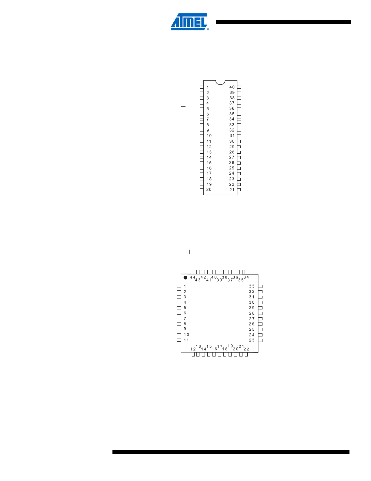
Pin Configurations
Figure 1-1.
Pinout ATmega644
Note:
The large center pad underneath the QFN/MLF package should be soldered to ground on the
board to ensure good mechanical stability.
(PCINT8/XCK0/T0) PB0
(PCINT9/CLKO/T1) PB1
(PCINT10/INT2/AIN0) PB2
(PCINT11/OC0A/AIN1) PB3
(PCINT12/OC0B/SS) PB4
(PCINT13/MOSI) PB5
(PCINT14/MISO) PB6
(PCINT15/SCK) PB7
RESET
VCC
GND
XTAL2
XTAL1
(PCINT24/RXD0) PD0
(PCINT25/TXD0) PD1
(PCINT26/INT0) PD2
(PCINT27/INT1) PD3
(PCINT28/OC1B) PD4
(PCINT29/OC1A) PD5
(PCINT30/OC2B/ICP) PD6
PA0 (ADC0/PCINT0)
PA1 (ADC1/PCINT1)
PA2 (ADC2/PCINT2)
PA3 (ADC3/PCINT3)
PA4 (ADC4/PCINT4)
PA5 (ADC5/PCINT5)
PA6 (ADC6/PCINT6)
PA7 (ADC7/PCINT7)
AREF
GND
AVCC
PC7 (TOSC2/PCINT23)
PC6 (TOSC1/PCINT22)
PC5 (TDI/PCINT21)
PC4 (TDO/PCINT20)
PC3 (TMS/PCINT19)
PC2 (TCK/PCINT18)
PC1 (SDA/PCINT17)
PC0 (SCL/PCINT16)
PD7 (OC2A/PCINT31)
PA4 (ADC4/PCINT4)
PA5 (ADC5/PCINT5)
PA6 (ADC6/PCINT6)
PA7 (ADC7/PCINT7)
AREF
GND
AVCC
PC7 (TOSC2/PCINT23)
PC6 (TOSC1/PCINT22)
PC5 (TDI/PCINT21)
PC4 (TDO/PCINT20)
(PCINT13/MOSI) PB5
(PCINT14/MISO) PB6
(PCINT15/SCK) PB7
RESET
VCC
GND
XTAL2
XTAL1
(PCINT24/RXD0) PD0
(PCINT25/TXD0) PD1
(PCINT26/INT0) PD2
(PCINT27/INT1) PD3 (PCINT28/OC1B) PD4 (PCINT29/OC1A) PD5
(PCINT30/OC2B/ICP) PD6
(PCINT31/OC2A) PD7
VCC GND
(PCINT16/SCL) PC0 (PCINT17/SDA) PC1 (PCINT18/TCK) PC2 (PCINT19/TMS) PC3
PB4 (SS/OC0B/PCINT12) PB3 (AIN1/OC0A/PCINT1
1)
PB2 (AIN0/INT2/PCINT10) PB1 (T1/CLKO/PCINT9) PB0 (XCK0/T0/PCINT8) GND VCC PA
0 (ADC0/PCINT0)
PA
1 (ADC1/PCINT1)
PA
2 (ADC2/PCINT2)
PA
3 (ADC3/PCINT3)
PDIP
TQFP/QFN/MLF
3
2593OS–AVR–02/12
ATmega644
1.1
Disclaimer
Typical values contained in this datasheet are based on simulations and characterization of
other AVR microcontrollers manufactured on the same process technology. Min and Max values
will be available after the device is characterized.
2.
Overview
The ATmega644 is a low-power CMOS 8-bit microcontroller based on the AVR enhanced RISC
architecture. By executing powerful instructions in a single clock cycle, the ATmega644
achieves throughputs approaching 1 MIPS per MHz allowing the system designer to optimize
power consumption versus processing speed.
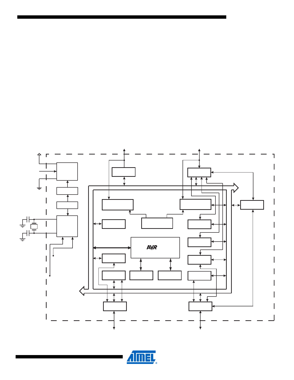
2.1
Block Diagram
Figure 2-1.
Block Diagram
CPU
GND
VCC
RESET
Power
Supervision
POR / BOD &
RESET
Watchdog
Oscillator
Watchdog
Timer
Oscillator
Circuits /
Clock
Generation
XTAL1
XTAL2
PORT A (8)
PORT D (8)
PD7..0
PORT C (8)
PC7..0
TWI
SPI
EEPROM
JTAG
8 bit T/C 0
8 bit T/C 2
16 bit T/C 1
SRAM
FLASH
USART 0
Internal
Bandgap reference
Analog
Comparator
A/D
Converter
PA7..0
PORT B (8)
PB7..0

4
2593OS–AVR–02/12
ATmega644
The AVR core combines a rich instruction set with 32 general purpose working registers. All the
32 registers are directly connected to the Arithmetic Logic Unit (ALU), allowing two independent
registers to be accessed in one single instruction executed in one clock cycle. The resulting
architecture is more code efficient while achieving throughputs up to ten times faster than con-
ventional CISC microcontrollers.
The ATmega644 provides the following features: 64 Kbytes of In-System Programmable Flash
with Read-While-Write capabilities, 2 Kbytes EEPROM, 4 Kbytes SRAM, 32 general purpose I/O
lines, 32 general purpose working registers, Real Time Counter (RTC), three flexible
Timer/Counters with compare modes and PWM, 2 USARTs, a byte oriented 2-wire Serial Inter-
face, a 8-channel, 10-bit ADC with optional differential input stage with programmable gain,
programmable Watchdog Timer with Internal Oscillator, an SPI serial port, IEEE std. 1149.1
compliant JTAG test interface, also used for accessing the On-chip Debug system and program-
ming and six software selectable power saving modes. The Idle mode stops the CPU while
allowing the SRAM, Timer/Counters, SPI port, and interrupt system to continue functioning. The
Power-down mode saves the register contents but freezes the Oscillator, disabling all other chip
functions until the next interrupt or Hardware Reset. In Power-save mode, the asynchronous
timer continues to run, allowing the user to maintain a timer base while the rest of the device is
sleeping. The ADC Noise Reduction mode stops the CPU and all I/O modules except Asynchro-
nous Timer and ADC, to minimize switching noise during ADC conversions. In Standby mode,
the Crystal/Resonator Oscillator is running while the rest of the device is sleeping. This allows
very fast start-up combined with low power consumption. In Extended Standby mode, both the
main Oscillator and the Asynchronous Timer continue to run.
The device is manufactured using Atmel’s high-density nonvolatile memory technology. The On-
chip ISP Flash allows the program memory to be reprogrammed in-system through an SPI serial
interface, by a conventional nonvolatile memory programmer, or by an On-chip Boot program
running on the AVR core. The boot program can use any interface to download the application
program in the application Flash memory. Software in the Boot Flash section will continue to run
while the Application Flash section is updated, providing true Read-While-Write operation. By
combining an 8-bit RISC CPU with In-System Self-Programmable Flash on a monolithic chip,
the Atmel ATmega644 is a powerful microcontroller that provides a highly flexible and cost effec-
tive solution to many embedded control applications.
The ATmega644 AVR is supported with a full suite of program and system development tools
including: C compilers, macro assemblers, program debugger/simulators, in-circuit emulators,
and evaluation kits.
2.2
Pin Descriptions
2.2.1
VCC
Digital supply voltage.
2.2.2
GND
Ground.
2.2.3
Port A (PA7:PA0)
Port A serves as analog inputs to the Analog-to-digital Converter.
Port A also serves as an 8-bit bi-directional I/O port with internal pull-up resistors (selected for
each bit). The Port A output buffers have symmetrical drive characteristics with both high sink

5
2593OS–AVR–02/12
ATmega644
and source capability. As inputs, Port A pins that are externally pulled low will source current if
the pull-up resistors are activated. The Port A pins are tri-stated when a reset condition becomes
active, even if the clock is not running.
Port A also serves the functions of various special features of the ATmega644 as listed on
page
73
.
2.2.4
Port B (PB7:PB0)
Port B is an 8-bit bi-directional I/O port with internal pull-up resistors (selected for each bit). The
Port B output buffers have symmetrical drive characteristics with both high sink and source
capability. As inputs, Port B pins that are externally pulled low will source current if the pull-up
resistors are activated. The Port B pins are tri-stated when a reset condition becomes active,
even if the clock is not running.
Port B also serves the functions of various special features of the ATmega644 as listed on
page
75
.
2.2.5
Port C (PC7:PC0)
Port C is an 8-bit bi-directional I/O port with internal pull-up resistors (selected for each bit). The
Port C output buffers have symmetrical drive characteristics with both high sink and source
capability. As inputs, Port C pins that are externally pulled low will source current if the pull-up
resistors are activated. The Port C pins are tri-stated when a reset condition becomes active,
even if the clock is not running.
Port C also serves the functions of the JTAG interface, along with special features of the
ATmega644 as listed on
page 78
.
2.2.6
Port D (PD7:PD0)
Port D is an 8-bit bi-directional I/O port with internal pull-up resistors (selected for each bit). The
Port D output buffers have symmetrical drive characteristics with both high sink and source
capability. As inputs, Port D pins that are externally pulled low will source current if the pull-up
resistors are activated. The Port D pins are tri-stated when a reset condition becomes active,
even if the clock is not running.
Port D also serves the functions of various special features of the ATmega644 as listed on
page
80
.
2.2.7
RESET
Reset input. A low level on this pin for longer than the minimum pulse length will generate a
reset, even if the clock is not running. The minimum pulse length is given in
”System and Reset
Characteristics” on page 320
. Shorter pulses are not guaranteed to generate a reset.
2.2.8
XTAL1
Input to the inverting Oscillator amplifier and input to the internal clock operating circuit.
2.2.9
XTAL2
Output from the inverting Oscillator amplifier.

6
2593OS–AVR–02/12
ATmega644
2.2.10
AVCC
AVCC is the supply voltage pin for Port F and the Analog-to-digital Converter. It should be exter-
nally connected to V
CC
, even if the ADC is not used. If the ADC is used, it should be connected
to V
CC
through a low-pass filter.
2.2.11
AREF
This is the analog reference pin for the Analog-to-digital Converter.

7
2593OS–AVR–02/12
ATmega644
3.
Resources
A comprehensive set of development tools, application notes and datasheetsare available for
download on http://www.atmel.com/avr.
8
2593OS–AVR–02/12
ATmega644
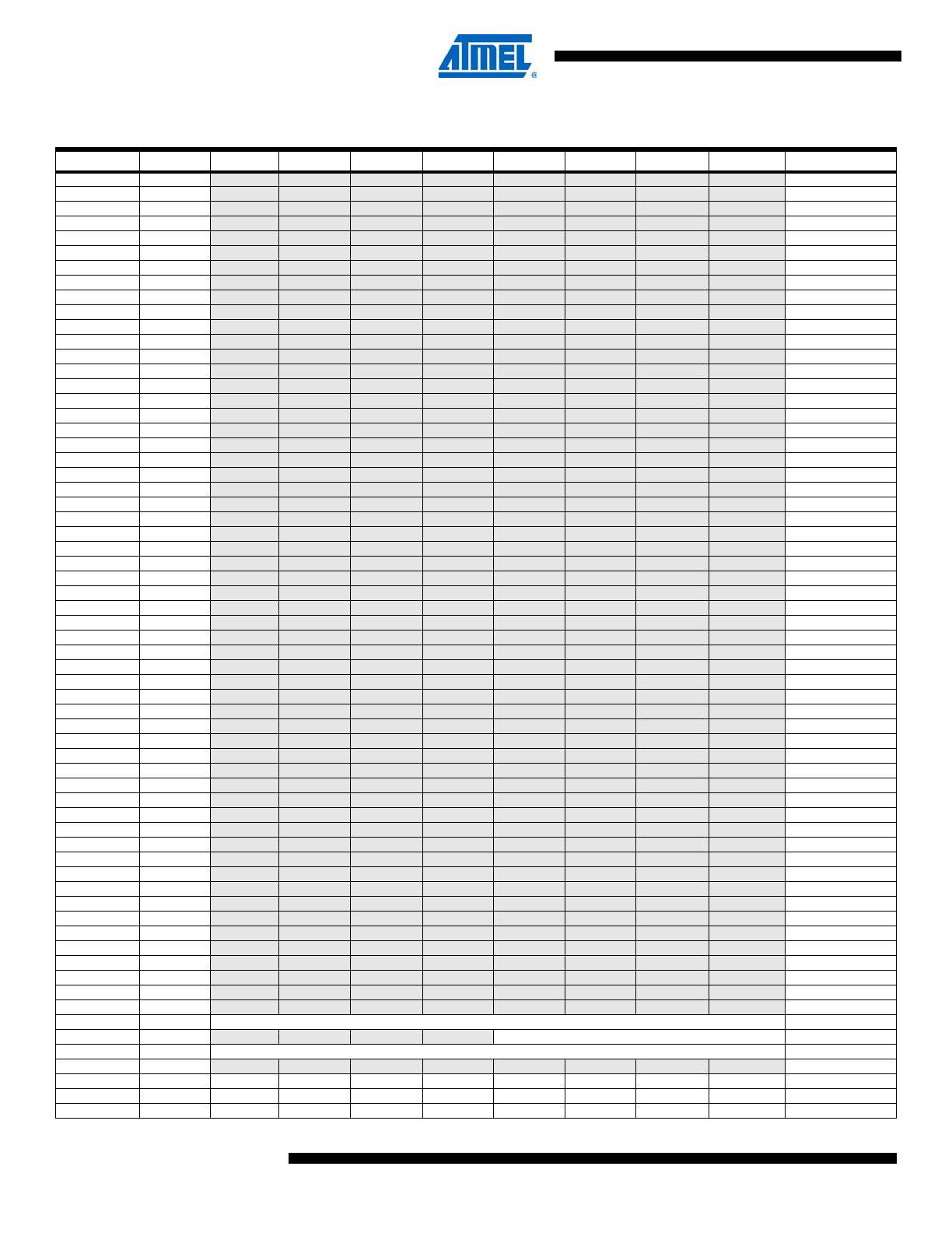
4.
Register Summary
Address
Name
Bit 7
Bit 6
Bit 5
Bit 4
Bit 3
Bit 2
Bit 1
Bit 0
Page
(0xFF)
Reserved
-
-
-
-
-
-
-
(0xFE)
Reserved
-
-
-
-
-
-
-
-
(0xFD)
Reserved
-
-
-
-
-
-
-
-
(0xFC)
Reserved
-
-
-
-
-
-
-
-
(0xFB)
Reserved
-
-
-
-
-
-
-
(0xFA)
Reserved
-
-
-
-
-
-
-
-
(0xF9)
Reserved
-
-
-
-
-
-
-
(0xF8)
Reserved
-
-
-
-
-
-
-
-
(0xF7)
Reserved
-
-
-
-
-
-
-
-
(0xF6)
Reserved
-
-
-
-
-
-
-
-
(0xF5)
Reserved
-
-
-
-
-
-
-
(0xF4)
Reserved
-
-
-
-
-
-
-
-
(0xF3)
Reserved
-
-
-
-
-
-
-
-
(0xF2)
Reserved
-
-
-
-
-
-
-
-
(0xF1)
Reserved
-
-
-
-
-
-
-
(0xF0)
Reserved
-
-
-
-
-
-
-
-
(0xEF)
Reserved
-
-
-
-
-
-
-
(0xEE)
Reserved
-
-
-
-
-
-
-
-
(0xED)
Reserved
-
-
-
-
-
-
-
-
(0xEC)
Reserved
-
-
-
-
-
-
-
-
(0xEB)
Reserved
-
-
-
-
-
-
-
(0xEA)
Reserved
-
-
-
-
-
-
-
-
(0xE9)
Reserved
-
-
-
-
-
-
-
-
(0xE8)
Reserved
-
-
-
-
-
-
-
-
(0xE7)
Reserved
-
-
-
-
-
-
-
(0xE6)
Reserved
-
-
-
-
-
-
-
-
(0xE5)
Reserved
-
-
-
-
-
-
-
-
(0xE4)
Reserved
-
-
-
-
-
-
-
-
(0xE3)
Reserved
-
-
-
-
-
-
-
(0xE2)
Reserved
-
-
-
-
-
-
-
-
(0xE1)
Reserved
-
-
-
-
-
-
-
(0xE0)
Reserved
-
-
-
-
-
-
-
(0xDF)
Reserved
-
-
-
-
-
-
-
-
(0xDE)
Reserved
-
-
-
-
-
-
-
-
(0xDD)
Reserved
-
-
-
-
-
-
-
-
(0xDC)
Reserved
-
-
-
-
-
-
-
(0xDB)
Reserved
-
-
-
-
-
-
-
-
(0xDA)
Reserved
-
-
-
-
-
-
-
-
(0xD9)
Reserved
-
-
-
-
-
-
-
-
(0xD8)
Reserved
-
-
-
-
-
-
-
-
(0xD7)
Reserved
-
-
-
-
-
-
-
-
(0xD6)
Reserved
-
-
-
-
-
-
-
-
(0xD5)
Reserved
-
-
-
-
-
-
-
-
(0xD4)
Reserved
-
-
-
-
-
-
-
-
(0xD3)
Reserved
-
-
-
-
-
-
-
-
(0xD2)
Reserved
-
-
-
-
-
-
-
-
(0xD1)
Reserved
-
-
-
-
-
-
-
-
(0xD0)
Reserved
-
-
-
-
-
-
-
-
(0xCF)
Reserved
-
-
-
-
-
-
-
-
(0xCE)
Reserved
-
-
-
-
-
-
-
-
(0xCD)
Reserved
-
-
-
-
-
-
-
-
(0xCC)
Reserved
-
-
-
-
-
-
-
-
(0xCB)
Reserved
-
-
-
-
-
-
-
-
(0xCA)
Reserved
-
-
-
-
-
-
-
-
(0xC9)
Reserved
-
-
-
-
-
-
-
-
(0xC8)
Reserved
-
-
-
-
-
-
-
-
(0xC7)
Reserved
-
-
-
-
-
-
-
-
(0xC6)
UDR0
USART0 I/O Data Register
182
(0xC5)
UBRR0H
-
-
-
-
USART0 Baud Rate Register High Byte
186/198
(0xC4)
UBRR0L
USART0 Baud Rate Register Low Byte
186/198
(0xC3)
Reserved
-
-
-
-
-
-
-
-
(0xC2)
UCSR0C
UMSEL01
UMSEL00
UPM01
UPM00
USBS0
UCSZ01
UCSZ00
UCPOL0
184/197
(0xC1)
UCSR0B
RXCIE0
TXCIE0
UDRIE0
RXEN0
TXEN0
UCSZ02
RXB80
TXB80
183/197
(0xC0)
UCSR0A
RXC0
TXC0
UDRE0
FE0
DOR0
UPE0
U2X0
MPCM0
182/196
9
2593OS–AVR–02/12
ATmega644
(0xBF)
Reserved
-
-
-
-
-
-
-
-
(0xBE)
Reserved
-
-
-
-
-
-
-
-
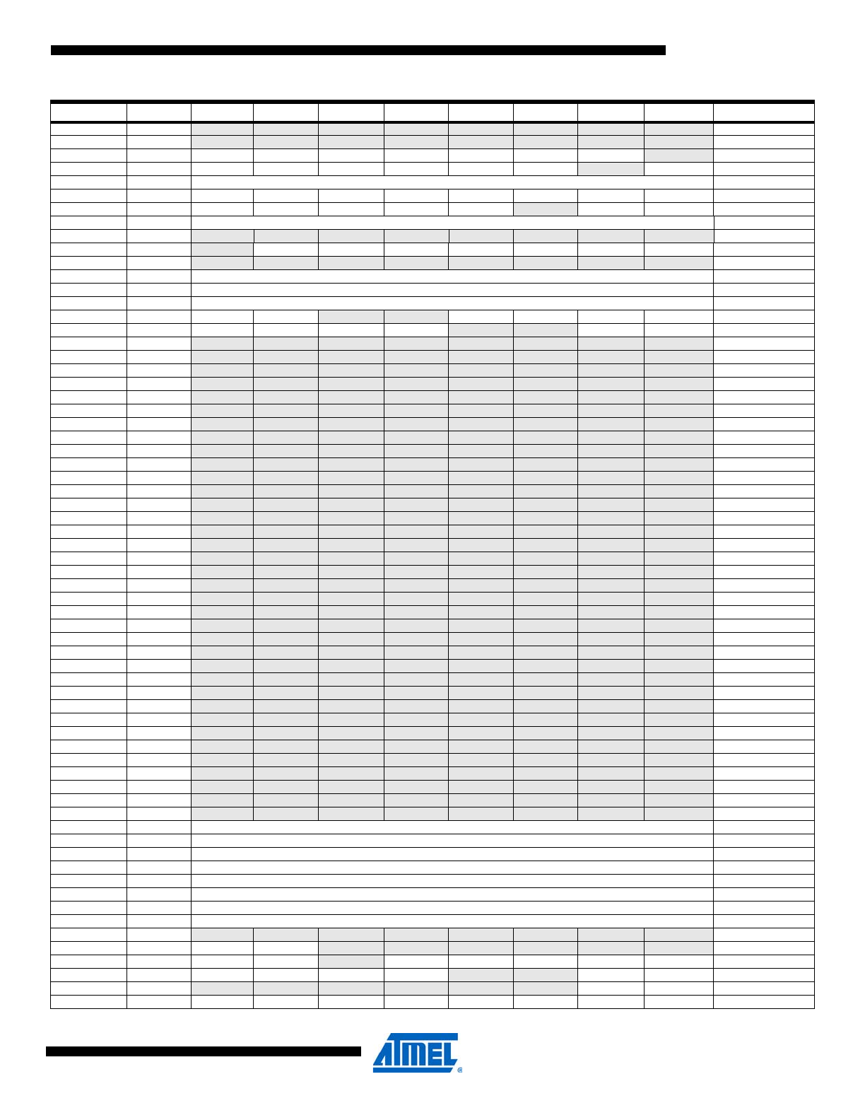
(0xBD)
TWAMR
TWAM6
TWAM5
TWAM4
TWAM3
TWAM2
TWAM1
TWAM0
-
228
(0xBC)
TWCR
TWINT
TWEA
TWSTA
TWSTO
TWWC
TWEN
-
TWIE
225
(0xBB)
TWDR
2-wire Serial Interface Data Register
227
(0xBA)
TWAR
TWA6
TWA5
TWA4
TWA3
TWA2
TWA1
TWA0
TWGCE
228
(0xB9)
TWSR
TWS7
TWS6
TWS5
TWS4
TWS3
-
TWPS1
TWPS0
227
(0xB8)
TWBR
2-wire Serial Interface Bit Rate Register
225
(0xB7)
Reserved
-
-
-
-
-
-
-
-
(0xB6)
ASSR
-
EXCLK
AS2
TCN2UB
OCR2AUB
OCR2BUB
TCR2AUB
TCR2BUB
150
(0xB5)
Reserved
-
-
-
-
-
-
-
-
(0xB4)
OCR2B
Timer/Counter2 Output Compare Register B
150
(0xB3)
OCR2A
Timer/Counter2 Output Compare Register A
150
(0xB2)
TCNT2
Timer/Counter2 (8 Bit)
150
(0xB1)
TCCR2B
FOC2A
FOC2B
-
-
WGM22
CS22
CS21
CS20
149
(0xB0)
TCCR2A
COM2A1
COM2A0
COM2B1
COM2B0
-
-
WGM21
WGM20
146
(0xAF)
Reserved
-
-
-
-
-
-
-
-
(0xAE)
Reserved
-
-
-
-
-
-
-
-
(0xAD)
Reserved
-
-
-
-
-
-
-
-
(0xAC)
Reserved
-
-
-
-
-
-
-
-
(0xAB)
Reserved
-
-
-
-
-
-
-
-
(0xAA)
Reserved
-
-
-
-
-
-
-
-
(0xA9)
Reserved
-
-
-
-
-
-
-
-
(0xA8)
Reserved
-
-
-
-
-
-
-
-
(0xA7)
Reserved
-
-
-
-
-
-
-
-
(0xA6)
Reserved
-
-
-
-
-
-
-
-
(0xA5)
Reserved
-
-
-
-
-
-
-
-
(0xA4)
Reserved
-
-
-
-
-
-
-
-
(0xA3)
Reserved
-
-
-
-
-
-
-
-
(0xA2)
Reserved
-
-
-
-
-
-
-
-
(0xA1)
Reserved
-
-
-
-
-
-
-
-
(0xA0)
Reserved
-
-
-
-
-
-
-
-
(0x9F)
Reserved
-
-
-
-
-
-
-
-
(0x9E)
Reserved
-
-
-
-
-
-
-
-
(0x9D)
Reserved
-
-
-
-
-
-
-
-
(0x9C)
Reserved
-
-
-
-
-
-
-
-
(0x9B)
Reserved
-
-
-
-
-
-
-
-
(0x9A)
Reserved
-
-
-
-
-
-
-
-
(0x99)
Reserved
-
-
-
-
-
-
-
-
(0x98)
Reserved
-
-
-
-
-
-
-
-
(0x97)
Reserved
-
-
-
-
-
-
-
-
(0x96)
Reserved
-
-
-
-
-
-
-
-
(0x95)
Reserved
-
-
-
-
-
-
-
-
(0x94)
Reserved
-
-
-
-
-
-
-
-
(0x93)
Reserved
-
-
-
-
-
-
-
-
(0x92)
Reserved
-
-
-
-
-
-
-
-
(0x91)
Reserved
-
-
-
-
-
-
-
-
(0x90)
Reserved
-
-
-
-
-
-
-
-
(0x8F)
Reserved
-
-
-
-
-
-
-
-
(0x8E)
Reserved
-
-
-
-
-
-
-
-
(0x8D)
Reserved
-
-
-
-
-
-
-
-
(0x8C)
Reserved
-
-
-
-
-
-
-
-
(0x8B)
OCR1BH
Timer/Counter1 - Output Compare Register B High Byte
129
(0x8A)
OCR1BL
Timer/Counter1 - Output Compare Register B Low Byte
129
(0x89)
OCR1AH
Timer/Counter1 - Output Compare Register A High Byte
129
(0x88)
OCR1AL
Timer/Counter1 - Output Compare Register A Low Byte
129
(0x87)
ICR1H
Timer/Counter1 - Input Capture Register High Byte
130
(0x86)
ICR1L
Timer/Counter1 - Input Capture Register Low Byte
130
(0x85)
TCNT1H
Timer/Counter1 - Counter Register High Byte
129
(0x84)
TCNT1L
Timer/Counter1 - Counter Register Low Byte
129
(0x83)
Reserved
-
-
-
-
-
-
-
-
(0x82)
TCCR1C
FOC1A
FOC1B
-
-
-
-
-
-
128
(0x81)
TCCR1B
ICNC1
ICES1
-
WGM13
WGM12
CS12
CS11
CS10
127
(0x80)
TCCR1A
COM1A1
COM1A0
COM1B1
COM1B0
-
-
WGM11
WGM10
125
(0x7F)
DIDR1
-
-
-
-
-
-
AIN1D
AIN0D
232
(0x7E)
DIDR0
ADC7D
ADC6D
ADC5D
ADC4D
ADC3D
ADC2D
ADC1D
ADC0D
252
Address
Name
Bit 7
Bit 6
Bit 5
Bit 4
Bit 3
Bit 2
Bit 1
Bit 0
Page
10
2593OS–AVR–02/12
ATmega644
(0x7D)
Reserved
-
-
-
-
-
-
-
-
(0x7C)
ADMUX
REFS1
REFS0
ADLAR
MUX4
MUX3
MUX2
MUX1
MUX0
248
(0x7B)
ADCSRB
-
ACME
-
-
-
ADTS2
ADTS1
ADTS0
231
(0x7A)
ADCSRA
ADEN
ADSC
ADATE
ADIF
ADIE
ADPS2
ADPS1
ADPS0
249
(0x79)
ADCH
ADC Data Register High byte
251
(0x78)
ADCL
ADC Data Register Low byte
251
(0x77)
Reserved
-
-
-
-
-
-
-
-
(0x76)
Reserved
-
-
-
-
-
-
-
-
(0x75)
Reserved
-
-
-
-
-
-
-
-
(0x74)
Reserved
-
-
-
-
-
-
-
-
(0x73)
PCMSK3
PCINT31
PCINT30
PCINT29
PCINT28
PCINT27
PCINT26
PCINT25
PCINT24
63
(0x72)
Reserved
-
-
-
-
-
-
-
-
(0x71)
Reserved
-
-
-
-
-
-
-
-
(0x70)
TIMSK2
-
-
-
-
-
OCIE2B
OCIE2A
TOIE2
152
(0x6F)
TIMSK1
-
-
ICIE1
-
-
OCIE1B
OCIE1A
TOIE1
130
(0x6E)
TIMSK0
-
-
-
-
-
OCIE0B
OCIE0A
TOIE0
101
(0x6D)
PCMSK2
PCINT23
PCINT22
PCINT21
PCINT20
PCINT19
PCINT18
PCINT17
PCINT16
63
(0x6C)
PCMSK1
PCINT15
PCINT14
PCINT13
PCINT12
PCINT11
PCINT10
PCINT9
PCINT8
63
(0x6B)
PCMSK0
PCINT7
PCINT6
PCINT5
PCINT4
PCINT3
PCINT2
PCINT1
PCINT0
64
(0x6A)
Reserved
-
-
-
-
-
-
-
-
(0x69)
EICRA
-
-
ISC21
ISC20
ISC11
ISC10
ISC01
ISC00
60
(0x68)
PCICR
-
-
-
-
PCIE3
PCIE2
PCIE1
PCIE0
62
(0x67)
Reserved
-
-
-
-
-
-
-
-
(0x66)
OSCCAL
Oscillator Calibration Register
37
(0x65)
Reserved
-
-
-
-
-
-
-
-
(0x64)
PRR
PRTWI
PRTIM2
PRTIM0
-
PRTIM1
PRSPI
PRUSART0
PRADC
44
(0x63)
Reserved
-
-
-
-
-
-
-
-
(0x62)
Reserved
-
-
-
-
-
-
-
-
(0x61)
CLKPR
CLKPCE
-
-
-
CLKPS3
CLKPS2
CLKPS1
CLKPS0
37
(0x60)
WDTCSR
WDIF
WDIE
WDP3
WDCE
WDE
WDP2
WDP1
WDP0
52
0x3F (0x5F)
SREG
I
T
H
S
V
N
Z
C
11
0x3E (0x5E)
SPH
SP15
SP14
SP13
SP12
SP11
SP10
SP9
SP8
11
0x3D (0x5D)
SPL
SP7
SP6
SP5
SP4
SP3
SP2
SP1
SP0
11
0x3C (0x5C)
Reserved
-
-
-
-
-
-
-
-
0x3B (0x5B)
Reserved
-
-
-
-
-
-
-
-
0x3A (0x5A)
Reserved
-
-
-
-
-
-
-
-
0x39 (0x59)
Reserved
-
-
-
-
-
-
-
-
0x38 (0x58)
Reserved
-
-
-
-
-
-
-
-
0x37 (0x57)
SPMCSR
SPMIE
RWWSB
SIGRD
RWWSRE
BLBSET
PGWRT
PGERS
SPMEN
281
0x36 (0x56)
Reserved
-
-
-
-
-
-
-
-
0x35 (0x55)
MCUCR
JTD
-
-
PUD
-
-
IVSEL
IVCE
84/267
0x34 (0x54)
MCUSR
-
-
-
JTRF
WDRF
BORF
EXTRF
PORF
52/268
0x33 (0x53)
SMCR
-
-
-
-
SM2
SM1
SM0
SE
43
0x32 (0x52)
Reserved
-
-
-
-
-
-
-
-
0x31 (0x51)
OCDR
On-Chip Debug Register
258
0x30 (0x50)
ACSR
ACD
ACBG
ACO
ACI
ACIE
ACIC
ACIS1
ACIS0
249
0x2F (0x4F)
Reserved
-
-
-
-
-
-
-
-
0x2E (0x4E)
SPDR
SPI 0 Data Register
163
0x2D (0x4D)
SPSR
SPIF
WCOL
-
-
-
-
-
SPI2X
162
0x2C (0x4C)
SPCR
SPIE
SPE
DORD
MSTR
CPOL
CPHA
SPR1
SPR0
161
0x2B (0x4B)
GPIOR2
General Purpose I/O Register 2
25
0x2A (0x4A)
GPIOR1
General Purpose I/O Register 1
25
0x29 (0x49)
Reserved
-
-
-
-
-
-
-
-
0x28 (0x48)
OCR0B
Timer/Counter0 Output Compare Register B
101
0x27 (0x47)
OCR0A
Timer/Counter0 Output Compare Register A
101
0x26 (0x46)
TCNT0
Timer/Counter0 (8 Bit)
101
0x25 (0x45)
TCCR0B
FOC0A
FOC0B
-
-
WGM02
CS02
CS01
CS00
100
0x24 (0x44)
TCCR0A
COM0A1
COM0A0
COM0B1
COM0B0
-
-
WGM01
WGM00
101
0x23 (0x43)
GTCCR
TSM
-
-
-
-
-
PSRASY
PSRSYNC
153
0x22 (0x42)
EEARH
-
-
-
-
EEPROM Address Register High Byte
21
0x21 (0x41)
EEARL
EEPROM Address Register Low Byte
21
0x20 (0x40)
EEDR
EEPROM Data Register
21
0x1F (0x3F)
EECR
-
-
EEPM1
EEPM0
EERIE
EEMPE
EEPE
EERE
21
0x1E (0x3E)
GPIOR0
General Purpose I/O Register 0
26
0x1D (0x3D)
EIMSK
-
-
-
-
-
INT2
INT1
INT0
61
0x1C (0x3C)
EIFR
-
-
-
-
-
INTF2
INTF1
INTF0
61
Address
Name
Bit 7
Bit 6
Bit 5
Bit 4
Bit 3
Bit 2
Bit 1
Bit 0
Page