
Appendix A - ATmega64 specification at 105
°
C
This document contains information specific to devices operating at temperatures up
to 105
°
C. Only deviations are covered in this appendix, all other information can be
found in the complete datasheet. The complete datasheet can be found on
www.atmel.com
8-bit
Microcontroller
with 64K Bytes
In-System
Programmable
Flash
ATmega64
Appendix A
2490 - Appendix A–AVR–10/09
2
2490 - Appendix A–AVR–10/09
ATmega64
Electrical Characteristics
Absolute Maximum Ratings*
Operating Temperature.................................. -55
°
C to +125
°
C
*NOTICE:
Stresses beyond those listed under “Absolute
Maximum Ratings” may cause permanent dam-
age to the device. This is a stress rating only and
functional operation of the device at these or
other conditions beyond those indicated in the
operational sections of this specification is not
implied. Exposure to absolute maximum rating
conditions for extended periods may affect device
reliability.
Storage Temperature ..................................... -65°C to +150°C
Voltage on any Pin except RESET
with respect to Ground ................................-0.5V to V
CC
+0.5V
Voltage on RESET with respect to Ground......-0.5V to +13.0V
Maximum Operating Voltage ............................................ 6.0V
DC Current per I/O Pin ............................................... 40.0 mA
DC Current
V
CC
and GND Pins................................ 200.0 mA
DC Characteristics
T
A
= -40
°
C to 105
°
C, V
CC
= 2.7V to 5.5V (unless otherwise noted)
Symbol
Parameter
Condition
Min
Typ
Max
Units
V
IL
Input Low Voltage
Except XTAL1 and
RESET pins
-0.5
0.2 V
CC
(1)
V
V
IL1
Input Low Voltage
XTAL1 pin, External
Clock Selected
-0.5
0.1 V
CC
(1)
V
V
IL2
Input Low Voltage
RESET pin
-0.5
0.2 V
CC
(1)
V
V
IH
Input High Voltage
Except XTAL1 and
RESET pins
0.6 V
CC
(2)
V
CC
+ 0.5
V
V
IH1
Input High Voltage
XTAL1 pin, External
Clock Selected
0.7 V
CC
(2)
V
CC
+ 0.5
V
V
IH2
Input High Voltage
RESET pin
0.85 V
CC
(2)
V
CC
+ 0.5
V
V
OL
Output Low Voltage
(3)
(Ports A,B,C,D, E, F, G)
I
OL
= 20 mA, V
CC
= 5V
I
OL
= 10 mA, V
CC
= 3V
0.9
0.6
V
V
V
OH
Output High Voltage
(4)
(Ports A,B,C,D, E, F, G))
I
OH
= -20 mA, V
CC
= 5V
I
OH
= -10 mA, V
CC
= 3V
4.1
2.1
V
V
I
IL
Input Leakage
Current I/O Pin
Vcc = 5.5V, pin low
(absolute value)
1.0
µA
I
IH
Input Leakage
Current I/O Pin
Vcc = 5.5V, pin high
(absolute value)
1.0
µA
R
RST
Reset Pull-up Resistor
30
60
k
Ω
R
PEN
PEN Pull-up Resistor
20
60
k
Ω
R
PU
I/O Pin Pull-up Resistor
20
50
k
Ω
3
2490 - Appendix A–AVR–10/09
ATmega64
Notes:
1. “Max” means the highest value where the pin is guaranteed to be read as low
2. “Min” means the lowest value where the pin is guaranteed to be read as high
3. Although each I/O port can sink more than the test conditions (20 mA at V
CC
= 5V, 10 mA at V
CC
= 3V) under steady state
conditions (non-transient), the following must be observed:
TQFP and QFN/MLF Package:
1] The sum of all IOL, for all ports, should not exceed 400 mA.
2] The sum of all IOL, for ports A0 - A7, G2, C3 - C7 should not exceed 100 mA.
3] The sum of all IOL, for ports C0 - C2, G0 - G1, D0 - D7, XTAL2 should not exceed 100 mA.
4] The sum of all IOL, for ports B0 - B7, G3 - G4, E0 - E7 should not exceed 100 mA.
5] The sum of all IOL, for ports F0 - F7, should not exceed 100 mA.
If IOL exceeds the test condition, VOL may exceed the related specification. Pins are not guaranteed to sink current greater
than the listed test condition.
4. Although each I/O port can source more than the test conditions (20 mA at Vcc = 5V, 10 mA at Vcc = 3V) under steady state
conditions (non-transient), the following must be observed:
TQFP and QFN/MLF Package:
1] The sum of all IOH, for all ports, should not exceed 400 mA.
2] The sum of all IOH, for ports A0 - A7, G2, C3 - C7 should not exceed 100 mA.
3] The sum of all IOH, for ports C0 - C2, G0 - G1, D0 - D7, XTAL2 should not exceed 100 mA.
4] The sum of all IOH, for ports B0 - B7, G3 - G4, E0 - E7 should not exceed 100 mA.
5] The sum of all IOH, for ports F0 - F7, should not exceed 100 mA.
If IOH exceeds the test condition, VOH may exceed the related specification. Pins are not guaranteed to source current
greater than the listed test condition.
5. Minimum V
CC
for Power-down is 2.5V.
I
CC
Power Supply Current
Active 4 MHz, V
CC
= 3V
5
mA
Active 8 MHz, V
CC
= 5V
20
mA
Idle 4 MHz, V
CC
= 3V
3
mA
Idle 8 MHz, V
CC
= 5V
12
mA
Power-down mode
(5)
WDT enabled, V
CC
= 3V
< 15
30
µA
WDT disabled, V
CC
= 3V
< 5
20
µA
V
ACIO
Analog Comparator
Input Offset Voltage
V
CC
= 5V
V
in
= V
CC
/2
-40
40
mV
I
ACLK
Analog Comparator
Input Leakage Current
V
CC
= 5V
V
in
= V
CC
/2
-50
50
nA
t
ACPD
Analog Comparator
Propagation Delay
V
CC
= 2.7V
V
CC
= 5.0
750
500
ns
DC Characteristics
T
A
= -40
°
C to 105
°
C, V
CC
= 2.7V to 5.5V (unless otherwise noted) (Continued)
Symbol
Parameter
Condition
Min
Typ
Max
Units
4
2490 - Appendix A–AVR–10/09
ATmega64
ATmega64
Typical
Characteristics
– Preliminary
Data
The following charts show typical behavior. These figures are not tested during manufacturing.
All current consumption measurements are performed with all I/O pins configured as inputs and
with internal pull-ups enabled. A sine wave generator with rail-to-rail output is used as clock
source.
The power consumption in Power-down mode is independent of clock selection.
The current consumption is a function of several factors such as: operating voltage, operating
frequency, loading of I/O pins, switching rate of I/O pins, code executed and ambient tempera-
ture. The dominating factors are operating voltage and frequency.
The current drawn from capacitive loaded pins may be estimated (for one pin) as C
L
*
V
CC
*f where
C
L
= load capacitance, V
CC
= operating voltage and f = average switching frequency of I/O pin.
The parts are characterized at frequencies higher than test limits. Parts are not guaranteed to
function properly at frequencies higher than the ordering code indicates.
The difference between current consumption in Power-down mode with Watchdog Timer
enabled and Power-down mode with Watchdog Timer disabled represents the differential cur-
rent drawn by the Watchdog Timer.
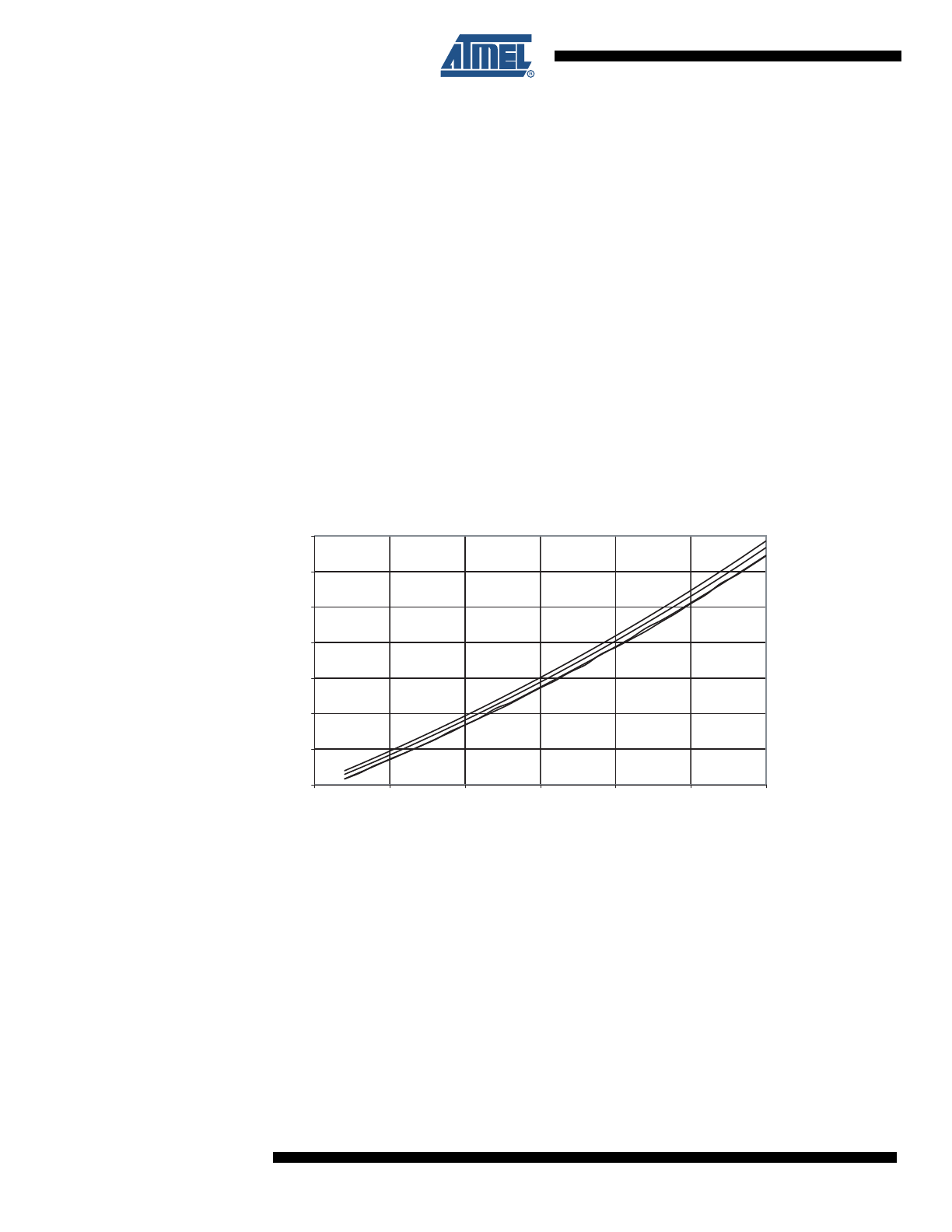
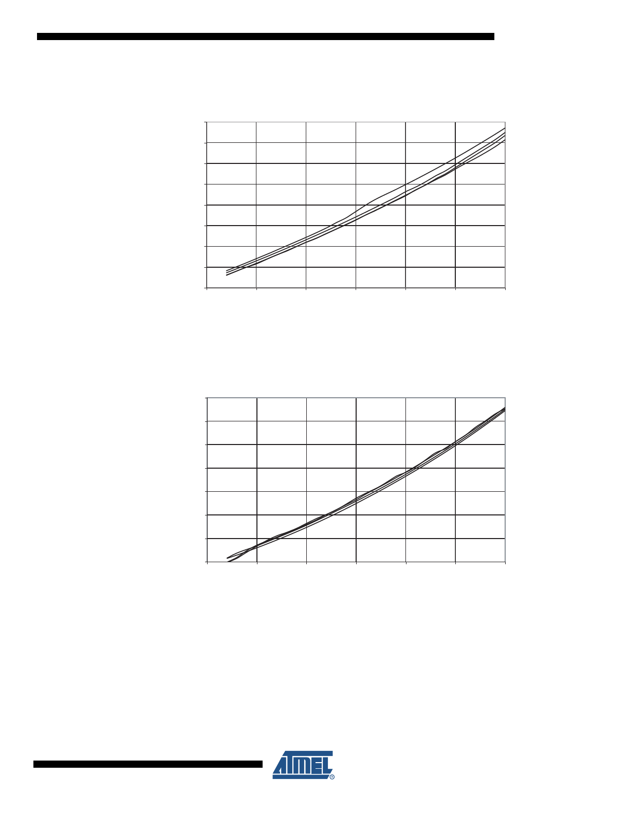
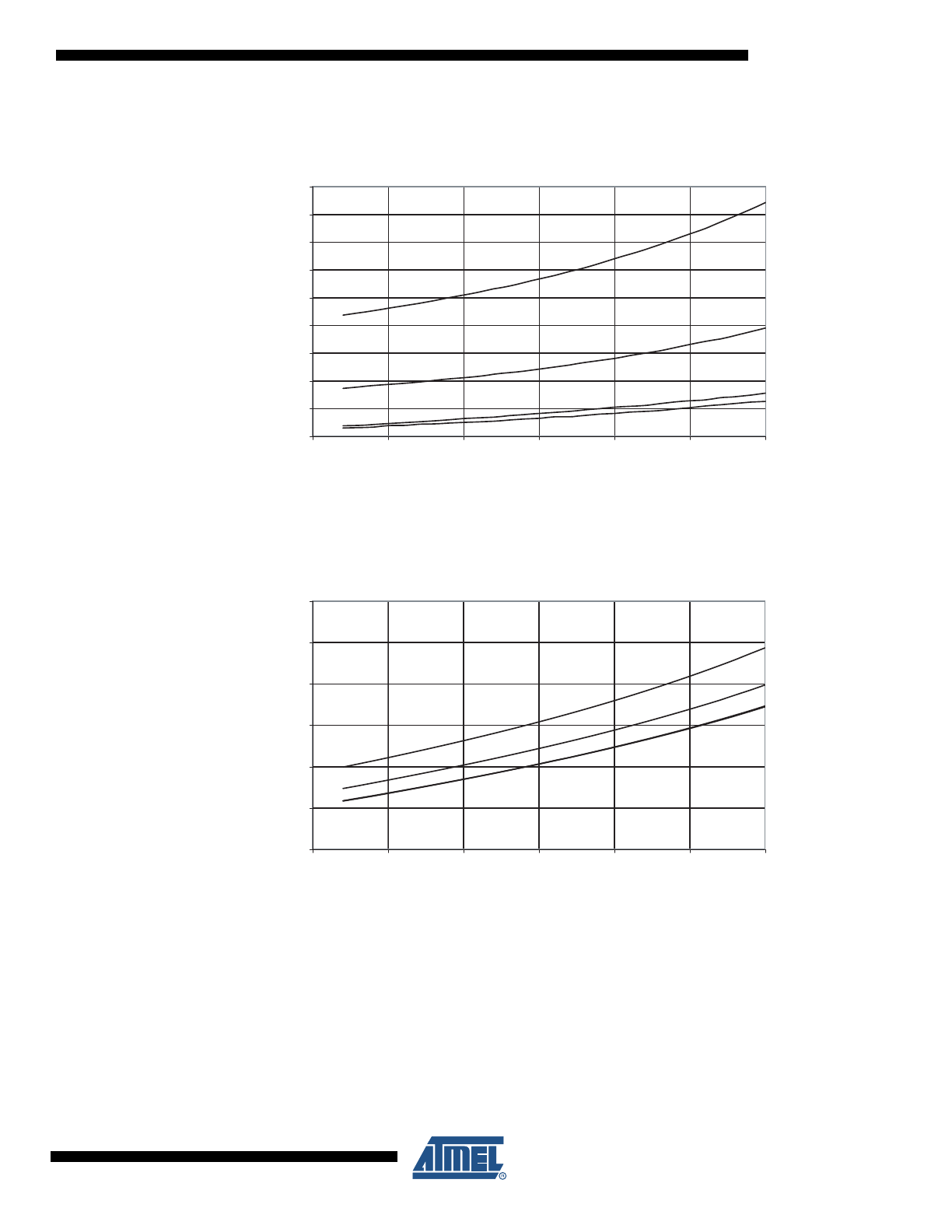
Active Supply Current
Figure 1. Active Supply Current vs. V
CC
(Internal RC Oscillator, 8 MHz)
ACTIVE SUPPLY CURRENT vs. Vcc
INTERNAL RC OSCILLATOR, 8 MHz
105 °C
85 °C
25 °C
-40 °C
6
8
10
12
14
16
18
20
2.5
3
3.5
4
4.5
5
5.5
Vcc (V)
I cc
(mA)
5
2490 - Appendix A–AVR–10/09
ATmega64
Figure 2. Active Supply Current vs. V
CC
(Internal RC Oscillator, 4 MHz)
Figure 3. Active Supply Current vs. V
CC
(Internal RC Oscillator, 2 kHz)
ACTIVE SUPPLY CURRENT vs. Vcc
INTERNAL RC OSCILLATOR, 4 MHz
105 °C
85 °C
25 °C
-40 °C
Vcc (V)
I cc
(mA)
3
4
5
6
7
8
9
10
11
2,5
3
3,5
4
4,5
5
5,5
ACTIVE SUPPLY CURRENT vs. Vcc
INTERNAL RC OSCILLATOR, 2 MHz
105 °C
85 °C
25 °C
-40 °C
2
2.5
3
3.5
4
4.5
5
5.5
2.5
3
3.5
4
4.5
5
5.5
Vcc (V)
I cc
(mA)
6
2490 - Appendix A–AVR–10/09
ATmega64
Figure 4. Active Supply Current vs. V
CC
(Internal RC Oscillator, 1 kHz)
Figure 5. Active Supply Current vs. V
CC
(Internal RC Oscillator, 1 kHz)
ACTIVE SUPPLY CURRENT vs. Vcc
INTERNAL RC OSCILLATOR, 1 MHz
105 °C
85 °C
25 °C
-40 °C
1
1.2
1.4
1.6
1.8
2
2.2
2.4
2.6
2.8
2.5
3
3.5
4
4.5
5
5.5
Vcc (V)
I cc
(mA)
ACTIVE SUPPLY CURRENT vs. Vcc
INTERNAL RC OSCILLATOR, 1 MHz
105 °C
85 °C
25 °C
-40 °C
1
1.2
1.4
1.6
1.8
2
2.2
2.4
2.6
2.8
2.5
3
3.5
4
4.5
5
5.5
Vcc (V)
I cc
(mA)
7
2490 - Appendix A–AVR–10/09
ATmega64
Idle Supply Current
Figure 6. Idle Supply Current vs. V
CC
(Internal RC Oscillator, 1 MHz)
Figure 7. Idle Supply Current vs. V
CC
(Internal RC Oscillator, 2 MHz)
IDLE SUPPLY CURRENT vs. Vcc
INTERNAL RC OSCILLATOR, 1 MHz
105 °C
85 °C
25 °C
-40 °C
0.4
0.6
0.8
1
1.2
1.4
1.6
2.5
3
3.5
4
4.5
5
5.5
Vcc (V)
I cc
(mA)
IDLE SUPPLY CURRENT vs. Vcc
INTERNAL RC OSCILLATOR, 2 MHz
105 °C
85 °C
25 °C
-40 °C
0.5
1
1.5
2
2.5
3
2.5
3
3.5
4
4.5
5
5.5
Vcc (V)
I cc
(mA)
8
2490 - Appendix A–AVR–10/09
ATmega64
Figure 8. Idle Supply Current vs. V
CC
(Internal RC Oscillator, 4 MHz)
Figure 9. Idle Supply Current vs. V
CC
(Internal RC Oscillator, 8 MHz)
IDLE SUPPLY CURRENT vs. Vcc
INTERNAL RC OSCILLATOR, 4 MHz
105 °C
85 °C
25 °C
-40 °C
1.5
2
2.5
3
3.5
4
4.5
5
5.5
6
2.5
3
3.5
4
4.5
5
5.5
Vcc (V)
I cc
(mA)
IDLE SUPPLY CURRENT vs. Vcc
INTERNAL RC OSCILLATOR, 8 MHz
105 °C
85 °C
25 °C
-40 °C
3
4
5
6
7
8
9
10
11
2.5
3
3.5
4
4.5
5
5.5
Vcc (V)
I cc
(mA)
9
2490 - Appendix A–AVR–10/09
ATmega64
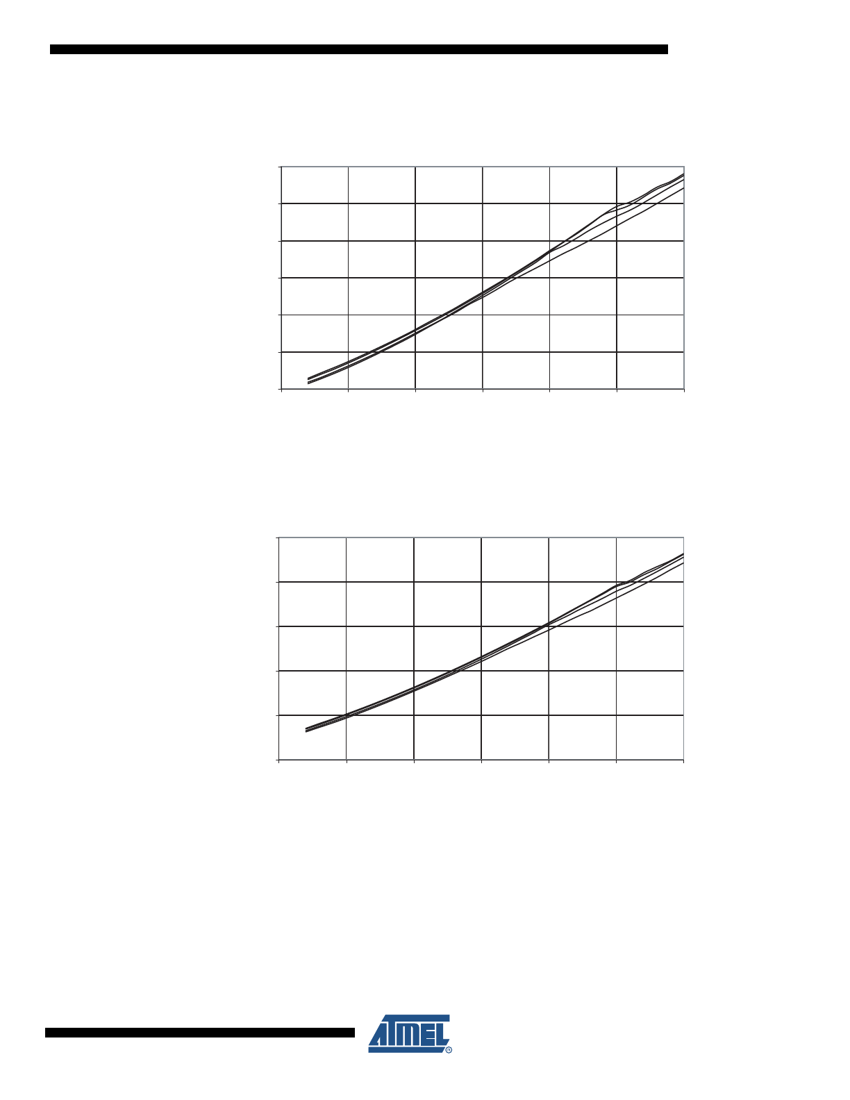
Power-Down Supply
Current
Figure 10. Power-Down Supply Current vs. V
CC
(Watchdog Timer Disabled)
Figure 11. Power-Down Supply Current vs. V
CC
(Watchdog Timer Enabled)
POWER-DOWN SUPPLY CURRENT vs. Vcc
WATCHDOG TIMER DISABLED
105 °C
85 °C
25 °C
-40 °C
0
1
2
3
4
5
6
7
8
9
2.5
3
3.5
4
4.5
5
5.5
Vcc (V)
I cc
(uA
)
POWER-DOWN SUPPLY CURRENT vs. Vcc
WATCHDOG TIMER ENABLED
105 °C
85 °C
25 °C
-40 °C
0
5
10
15
20
25
30
2.5
3
3.5
4
4.5
5
5.5
Vcc (V)
I cc
(uA)
10
2490 - Appendix A–AVR–10/09
ATmega64
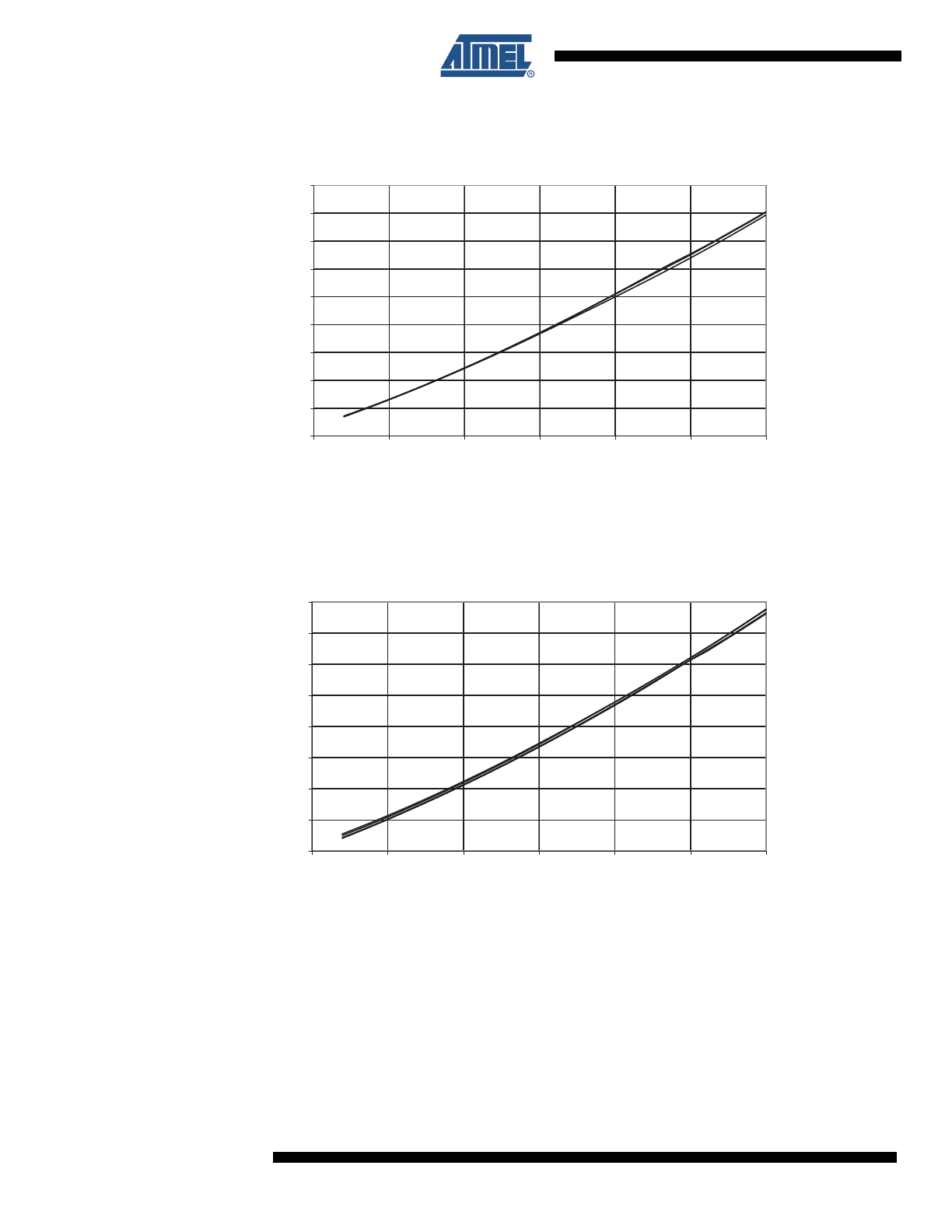
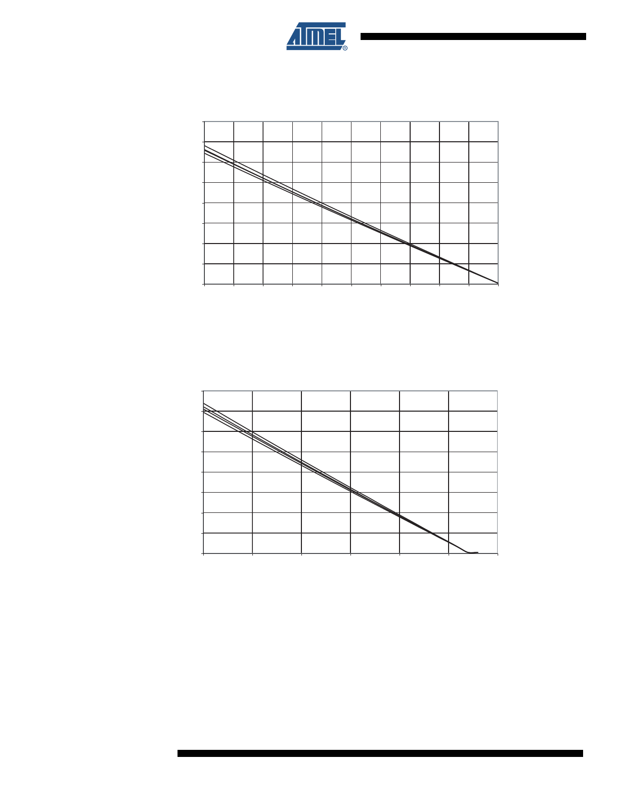
Pin Pull-up
Figure 12. I/O Pin Pull-Up Resistor Current vs. Input Voltage (V
CC
= 5V)
Figure 13. I/O Pin Pull-Up Resistor Current vs. Input Voltage (V
CC
= 2.7V)
I/O PIN PULL-UP RESISTOR CURRENT vs. INPUT VOLTAGE
Vcc = 5V
105 °C
85 °C
25 °C
-40 °C
0
20
40
60
80
100
120
140
160
0
0.5
1
1.5
2
2.5
3
3.5
4
4.5
5
V
OP
(V)
I
OP
(uA)
I/O PIN PULL-UP RESISTOR CURRENT vs. INPUT VOLTAGE
Vcc = 2.7V
105 °C
85 °C
25 °C
-40 °C
0
10
20
30
40
50
60
70
80
0
0.5
1
1.5
2
2.5
3
V
OP
(V)
I
OP
(uA)
Appendix A - ATmega64 specification at 105
°
C
This document contains information specific to devices operating at temperatures up
to 105
°
C. Only deviations are covered in this appendix, all other information can be
found in the complete datasheet. The complete datasheet can be found on
www.atmel.com
8-bit
Microcontroller
with 64K Bytes
In-System
Programmable
Flash
ATmega64
Appendix A
2490 - Appendix A–AVR–10/09
2
2490 - Appendix A–AVR–10/09
ATmega64
Electrical Characteristics
Absolute Maximum Ratings*
Operating Temperature.................................. -55
°
C to +125
°
C
*NOTICE:
Stresses beyond those listed under “Absolute
Maximum Ratings” may cause permanent dam-
age to the device. This is a stress rating only and
functional operation of the device at these or
other conditions beyond those indicated in the
operational sections of this specification is not
implied. Exposure to absolute maximum rating
conditions for extended periods may affect device
reliability.
Storage Temperature ..................................... -65°C to +150°C
Voltage on any Pin except RESET
with respect to Ground ................................-0.5V to V
CC
+0.5V
Voltage on RESET with respect to Ground......-0.5V to +13.0V
Maximum Operating Voltage ............................................ 6.0V
DC Current per I/O Pin ............................................... 40.0 mA
DC Current
V
CC
and GND Pins................................ 200.0 mA
DC Characteristics
T
A
= -40
°
C to 105
°
C, V
CC
= 2.7V to 5.5V (unless otherwise noted)
Symbol
Parameter
Condition
Min
Typ
Max
Units
V
IL
Input Low Voltage
Except XTAL1 and
RESET pins
-0.5
0.2 V
CC
(1)
V
V
IL1
Input Low Voltage
XTAL1 pin, External
Clock Selected
-0.5
0.1 V
CC
(1)
V
V
IL2
Input Low Voltage
RESET pin
-0.5
0.2 V
CC
(1)
V
V
IH
Input High Voltage
Except XTAL1 and
RESET pins
0.6 V
CC
(2)
V
CC
+ 0.5
V
V
IH1
Input High Voltage
XTAL1 pin, External
Clock Selected
0.7 V
CC
(2)
V
CC
+ 0.5
V
V
IH2
Input High Voltage
RESET pin
0.85 V
CC
(2)
V
CC
+ 0.5
V
V
OL
Output Low Voltage
(3)
(Ports A,B,C,D, E, F, G)
I
OL
= 20 mA, V
CC
= 5V
I
OL
= 10 mA, V
CC
= 3V
0.9
0.6
V
V
V
OH
Output High Voltage
(4)
(Ports A,B,C,D, E, F, G))
I
OH
= -20 mA, V
CC
= 5V
I
OH
= -10 mA, V
CC
= 3V
4.1
2.1
V
V
I
IL
Input Leakage
Current I/O Pin
Vcc = 5.5V, pin low
(absolute value)
1.0
µA
I
IH
Input Leakage
Current I/O Pin
Vcc = 5.5V, pin high
(absolute value)
1.0
µA
R
RST
Reset Pull-up Resistor
30
60
k
Ω
R
PEN
PEN Pull-up Resistor
20
60
k
Ω
R
PU
I/O Pin Pull-up Resistor
20
50
k
Ω
3
2490 - Appendix A–AVR–10/09
ATmega64
Notes:
1. “Max” means the highest value where the pin is guaranteed to be read as low
2. “Min” means the lowest value where the pin is guaranteed to be read as high
3. Although each I/O port can sink more than the test conditions (20 mA at V
CC
= 5V, 10 mA at V
CC
= 3V) under steady state
conditions (non-transient), the following must be observed:
TQFP and QFN/MLF Package:
1] The sum of all IOL, for all ports, should not exceed 400 mA.
2] The sum of all IOL, for ports A0 - A7, G2, C3 - C7 should not exceed 100 mA.
3] The sum of all IOL, for ports C0 - C2, G0 - G1, D0 - D7, XTAL2 should not exceed 100 mA.
4] The sum of all IOL, for ports B0 - B7, G3 - G4, E0 - E7 should not exceed 100 mA.
5] The sum of all IOL, for ports F0 - F7, should not exceed 100 mA.
If IOL exceeds the test condition, VOL may exceed the related specification. Pins are not guaranteed to sink current greater
than the listed test condition.
4. Although each I/O port can source more than the test conditions (20 mA at Vcc = 5V, 10 mA at Vcc = 3V) under steady state
conditions (non-transient), the following must be observed:
TQFP and QFN/MLF Package:
1] The sum of all IOH, for all ports, should not exceed 400 mA.
2] The sum of all IOH, for ports A0 - A7, G2, C3 - C7 should not exceed 100 mA.
3] The sum of all IOH, for ports C0 - C2, G0 - G1, D0 - D7, XTAL2 should not exceed 100 mA.
4] The sum of all IOH, for ports B0 - B7, G3 - G4, E0 - E7 should not exceed 100 mA.
5] The sum of all IOH, for ports F0 - F7, should not exceed 100 mA.
If IOH exceeds the test condition, VOH may exceed the related specification. Pins are not guaranteed to source current
greater than the listed test condition.
5. Minimum V
CC
for Power-down is 2.5V.
I
CC
Power Supply Current
Active 4 MHz, V
CC
= 3V
5
mA
Active 8 MHz, V
CC
= 5V
20
mA
Idle 4 MHz, V
CC
= 3V
3
mA
Idle 8 MHz, V
CC
= 5V
12
mA
Power-down mode
(5)
WDT enabled, V
CC
= 3V
< 15
30
µA
WDT disabled, V
CC
= 3V
< 5
20
µA
V
ACIO
Analog Comparator
Input Offset Voltage
V
CC
= 5V
V
in
= V
CC
/2
-40
40
mV
I
ACLK
Analog Comparator
Input Leakage Current
V
CC
= 5V
V
in
= V
CC
/2
-50
50
nA
t
ACPD
Analog Comparator
Propagation Delay
V
CC
= 2.7V
V
CC
= 5.0
750
500
ns
DC Characteristics
T
A
= -40
°
C to 105
°
C, V
CC
= 2.7V to 5.5V (unless otherwise noted) (Continued)
Symbol
Parameter
Condition
Min
Typ
Max
Units
4
2490 - Appendix A–AVR–10/09
ATmega64
ATmega64
Typical
Characteristics
– Preliminary
Data
The following charts show typical behavior. These figures are not tested during manufacturing.
All current consumption measurements are performed with all I/O pins configured as inputs and
with internal pull-ups enabled. A sine wave generator with rail-to-rail output is used as clock
source.
The power consumption in Power-down mode is independent of clock selection.
The current consumption is a function of several factors such as: operating voltage, operating
frequency, loading of I/O pins, switching rate of I/O pins, code executed and ambient tempera-
ture. The dominating factors are operating voltage and frequency.
The current drawn from capacitive loaded pins may be estimated (for one pin) as C
L
*
V
CC
*f where
C
L
= load capacitance, V
CC
= operating voltage and f = average switching frequency of I/O pin.
The parts are characterized at frequencies higher than test limits. Parts are not guaranteed to
function properly at frequencies higher than the ordering code indicates.
The difference between current consumption in Power-down mode with Watchdog Timer
enabled and Power-down mode with Watchdog Timer disabled represents the differential cur-
rent drawn by the Watchdog Timer.
Active Supply Current
Figure 1. Active Supply Current vs. V
CC
(Internal RC Oscillator, 8 MHz)
ACTIVE SUPPLY CURRENT vs. Vcc
INTERNAL RC OSCILLATOR, 8 MHz
105 °C
85 °C
25 °C
-40 °C
6
8
10
12
14
16
18
20
2.5
3
3.5
4
4.5
5
5.5
Vcc (V)
I cc
(mA)
5
2490 - Appendix A–AVR–10/09
ATmega64
Figure 2. Active Supply Current vs. V
CC
(Internal RC Oscillator, 4 MHz)
Figure 3. Active Supply Current vs. V
CC
(Internal RC Oscillator, 2 kHz)
ACTIVE SUPPLY CURRENT vs. Vcc
INTERNAL RC OSCILLATOR, 4 MHz
105 °C
85 °C
25 °C
-40 °C
Vcc (V)
I cc
(mA)
3
4
5
6
7
8
9
10
11
2,5
3
3,5
4
4,5
5
5,5
ACTIVE SUPPLY CURRENT vs. Vcc
INTERNAL RC OSCILLATOR, 2 MHz
105 °C
85 °C
25 °C
-40 °C
2
2.5
3
3.5
4
4.5
5
5.5
2.5
3
3.5
4
4.5
5
5.5
Vcc (V)
I cc
(mA)
6
2490 - Appendix A–AVR–10/09
ATmega64
Figure 4. Active Supply Current vs. V
CC
(Internal RC Oscillator, 1 kHz)
Figure 5. Active Supply Current vs. V
CC
(Internal RC Oscillator, 1 kHz)
ACTIVE SUPPLY CURRENT vs. Vcc
INTERNAL RC OSCILLATOR, 1 MHz
105 °C
85 °C
25 °C
-40 °C
1
1.2
1.4
1.6
1.8
2
2.2
2.4
2.6
2.8
2.5
3
3.5
4
4.5
5
5.5
Vcc (V)
I cc
(mA)
ACTIVE SUPPLY CURRENT vs. Vcc
INTERNAL RC OSCILLATOR, 1 MHz
105 °C
85 °C
25 °C
-40 °C
1
1.2
1.4
1.6
1.8
2
2.2
2.4
2.6
2.8
2.5
3
3.5
4
4.5
5
5.5
Vcc (V)
I cc
(mA)
7
2490 - Appendix A–AVR–10/09
ATmega64
Idle Supply Current
Figure 6. Idle Supply Current vs. V
CC
(Internal RC Oscillator, 1 MHz)
Figure 7. Idle Supply Current vs. V
CC
(Internal RC Oscillator, 2 MHz)
IDLE SUPPLY CURRENT vs. Vcc
INTERNAL RC OSCILLATOR, 1 MHz
105 °C
85 °C
25 °C
-40 °C
0.4
0.6
0.8
1
1.2
1.4
1.6
2.5
3
3.5
4
4.5
5
5.5
Vcc (V)
I cc
(mA)
IDLE SUPPLY CURRENT vs. Vcc
INTERNAL RC OSCILLATOR, 2 MHz
105 °C
85 °C
25 °C
-40 °C
0.5
1
1.5
2
2.5
3
2.5
3
3.5
4
4.5
5
5.5
Vcc (V)
I cc
(mA)
8
2490 - Appendix A–AVR–10/09
ATmega64
Figure 8. Idle Supply Current vs. V
CC
(Internal RC Oscillator, 4 MHz)
Figure 9. Idle Supply Current vs. V
CC
(Internal RC Oscillator, 8 MHz)
IDLE SUPPLY CURRENT vs. Vcc
INTERNAL RC OSCILLATOR, 4 MHz
105 °C
85 °C
25 °C
-40 °C
1.5
2
2.5
3
3.5
4
4.5
5
5.5
6
2.5
3
3.5
4
4.5
5
5.5
Vcc (V)
I cc
(mA)
IDLE SUPPLY CURRENT vs. Vcc
INTERNAL RC OSCILLATOR, 8 MHz
105 °C
85 °C
25 °C
-40 °C
3
4
5
6
7
8
9
10
11
2.5
3
3.5
4
4.5
5
5.5
Vcc (V)
I cc
(mA)
9
2490 - Appendix A–AVR–10/09
ATmega64
Power-Down Supply
Current
Figure 10. Power-Down Supply Current vs. V
CC
(Watchdog Timer Disabled)
Figure 11. Power-Down Supply Current vs. V
CC
(Watchdog Timer Enabled)
POWER-DOWN SUPPLY CURRENT vs. Vcc
WATCHDOG TIMER DISABLED
105 °C
85 °C
25 °C
-40 °C
0
1
2
3
4
5
6
7
8
9
2.5
3
3.5
4
4.5
5
5.5
Vcc (V)
I cc
(uA
)
POWER-DOWN SUPPLY CURRENT vs. Vcc
WATCHDOG TIMER ENABLED
105 °C
85 °C
25 °C
-40 °C
0
5
10
15
20
25
30
2.5
3
3.5
4
4.5
5
5.5
Vcc (V)
I cc
(uA)
10
2490 - Appendix A–AVR–10/09
ATmega64
Pin Pull-up
Figure 12. I/O Pin Pull-Up Resistor Current vs. Input Voltage (V
CC
= 5V)
Figure 13. I/O Pin Pull-Up Resistor Current vs. Input Voltage (V
CC
= 2.7V)
I/O PIN PULL-UP RESISTOR CURRENT vs. INPUT VOLTAGE
Vcc = 5V
105 °C
85 °C
25 °C
-40 °C
0
20
40
60
80
100
120
140
160
0
0.5
1
1.5
2
2.5
3
3.5
4
4.5
5
V
OP
(V)
I
OP
(uA)
I/O PIN PULL-UP RESISTOR CURRENT vs. INPUT VOLTAGE
Vcc = 2.7V
105 °C
85 °C
25 °C
-40 °C
0
10
20
30
40
50
60
70
80
0
0.5
1
1.5
2
2.5
3
V
OP
(V)
I
OP
(uA)