
Features
•
High Performance, Low Power Atmel
®
AVR
®
8-Bit Microcontroller
•
Advanced RISC Architecture
– 130 Powerful Instructions – Most Single Clock Cycle Execution
– 32 x 8 General Purpose Working Registers
– Fully Static Operation
– Up to 16 MIPS Throughput at 16MHz
– On-Chip 2-cycle Multiplier
•
High Endurance Non-volatile Memory Segments
– In-System Self-programmable Flash Program Memory
• 32KBytes (ATmega329/ATmega3290)
• 64KBytes (ATmega649/ATmega6490)
– EEPROM
• 1Kbytes (ATmega329/ATmega3290)
• 2Kbytes (ATmega649/ATmega6490)
– Internal SRAM
• 2Kbytes (ATmega329/ATmega3290)
• 4Kbytes (ATmega649/ATmega6490)
– Write/Erase Cycles: 10,000 Flash/ 100,000 EEPROM
– Data retention: 20 years at 85°C/100 years at 25°C
(1)
– Optional Boot Code Section with Independent Lock Bits
• In-System Programming by On-chip Boot Program
• True Read-While-Write Operation
– Programming Lock for Software Security
•
JTAG (IEEE std. 1149.1 compliant) Interface
– Boundary-scan Capabilities According to the JTAG Standard
– Extensive On-chip Debug Support
– Programming of Flash, EEPROM, Fuses, and Lock Bits through the JTAG Interface
•
Peripheral Features
– 4 x 25 Segment LCD Driver (ATmega329/ATmega649)
– 4 x 40 Segment LCD Driver (ATmega3290/ATmega6490)
– Two 8-bit Timer/Counters with Separate Prescaler and Compare Mode
– One 16-bit Timer/Counter with Separate Prescaler, Compare Mode, and Capture
Mode
– Real Time Counter with Separate Oscillator
– Four PWM Channels
– 8-channel, 10-bit ADC
– Programmable Serial USART
– Master/Slave SPI Serial Interface
– Universal Serial Interface with Start Condition Detector
– Programmable Watchdog Timer with Separate On-chip Oscillator
– On-chip Analog Comparator
– Interrupt and Wake-up on Pin Change
•
Special Microcontroller Features
– Power-on Reset and Programmable Brown-out Detection
– Internal Calibrated Oscillator
– External and Internal Interrupt Sources
– Five Sleep Modes: Idle, ADC Noise Reduction, Power-save, Power-down, and
Standby
•
I/O and Packages
– 53/68 Programmable I/O Lines
– 64-lead TQFP, 64-pad QFN/MLF, and 100-lead TQFP
•
Speed Grade:
– ATmega329V/ATmega3290V/ATmega649V/ATmega6490V:
– 0 - 4MHz @ 1.8 - 5.5V, 0 - 8MHz @ 2.7 - 5.5V
– ATmega329/3290/649/6490:
– 0 - 8MHz @ 2.7 - 5.5V, 0 - 16MHz @ 4.5 - 5.5V
•
Temperature range:
– -40°C to 85°C Industrial
•
Ultra-Low Power Consumption
– Active Mode:
• 1MHz, 1.8V: 350µA
• 32kHz, 1.8V: 20µA (including Oscillator)
• 32kHz, 1.8V: 40µA (including Oscillator and LCD)
– Power-down Mode:
• 100nA at 1.8V
8-bit Atmel
Microcontroller
with In-System
Programmable
Flash
ATmega329/V
ATmega3290/V
ATmega649/V
ATmega6490/V
Summary
2552KS–AVR–04/11
2
2552KS–AVR–04/11
ATmega329/3290/649/6490
1.
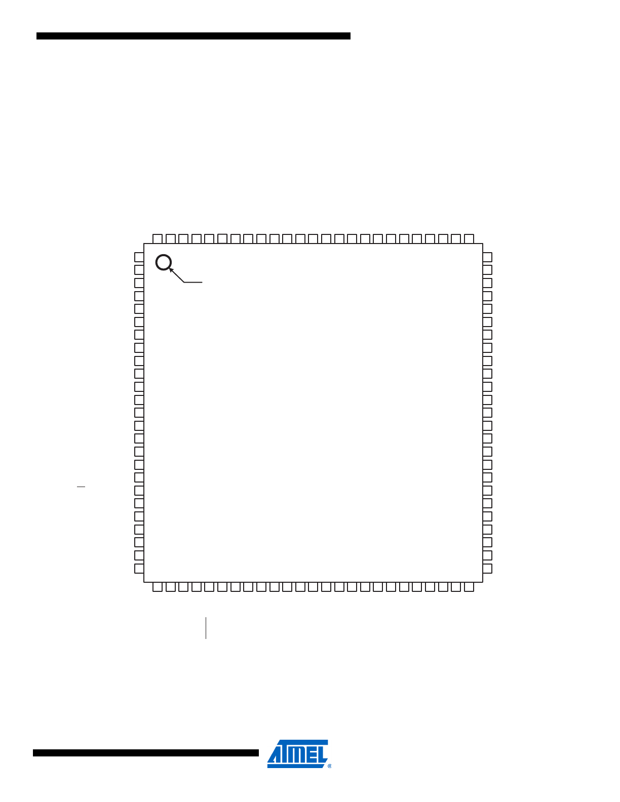
Pin Configurations
Figure 1-1.
Pinout ATmega3290/6490
(OC2A/PCINT15) PB7
DNC
(T1/SEG33) PG3
(T0/SEG32) PG4
RESET/PG5
V
CC
GND
(T
OSC2) XT
AL2
(T
OSC1) XT
AL1
DNC
DNC
(PCINT26/SEG31) PJ2
(PCINT27/SEG30) PJ3
(PCINT28/SEG29) PJ4
(PCINT29/SEG28) PJ5
(PCINT30/SEG27) PJ6
DNC
(ICP1/SEG26) PD0
(INT0/SEG25) PD1
(SEG24) PD2
(SEG23) PD3
(SEG22) PD4
(SEG21) PD5
(SEG20) PD6
(SEG19) PD7
A
V
CC
A
GND
AREF
PF0 (ADC0)
PF1 (ADC1)
PF2 (ADC2)
PF3 (ADC3)
PF4 (ADC4/TCK)
PF5 (ADC5/TMS)
PF6 (ADC6/TDO)
PF7 (ADC7/TDI)
DNC
DNC
PH7 (PCINT23/SEG36)
PH6 (PCINT22/SEG37)
PH5 (PCINT21/SEG38)
PH4 (PCINT20/SEG39)
DNC
DNC
GND
V
CC
DNC
P
A0 (COM0)
P
A1 (COM1)
P
A2 (COM2)
PA3 (COM3)
PA4 (SEG0)
PA5 (SEG1)
PA6 (SEG2)
PA7 (SEG3)
PG2 (SEG4)
PC7 (SEG5)
PC6 (SEG6)
DNC
PH3 (PCINT19/SEG7)
PH2 (PCINT18/SEG8)
PH1 (PCINT17/SEG9)
PH0 (PCINT16/SEG10)
DNC
DNC
DNC
DNC
PC5 (SEG11)
PC4 (SEG12)
PC3 (SEG13)
PC2 (SEG14)
PC1 (SEG15)
PC0 (SEG16)
PG1 (SEG17)
PG0 (SEG18)
INDEX CORNER
ATmega3290/6490
1
2
3
4
5
6
7
8
9
10
11
12
13
14
15
16
17
18
19
20
21
22
23
24
25
26
27
28
29
30
31
32
33
34
35
36
37
38
39
40
41
42
43
44
45
46
47
48
49
50
75
74
73
72
71
70
69
68
67
66
65
64
63
62
61
60
59
58
57
56
55
54
53
52
51
100
99
98
97
96
95
94
93
92
91
90
89
88
87
86
85
84
83
82
81
80
79
78
77
76
LCDCAP
(RXD/PCINT0) PE0
(TXD/PCINT1) PE1
(XCK/AIN0/PCINT2) PE2
(AIN1/PCINT3) PE3
(USCK/SCL/PCINT4) PE4
(DI/SDA/PCINT5) PE5
(DO/PCINT6) PE6
(CLKO/PCINT7) PE7
VCC
GND
DNC
(PCINT24/SEG35) PJ0
(PCINT25/SEG34) PJ1
DNC
DNC
DNC
DNC
(SS/PCINT8) PB0
(SCK/PCINT9) PB1
(MOSI/PCINT10) PB2
(MISO/PCINT11) PB3
(OC0A/PCINT12) PB4
(OC1A/PCINT13) PB5
(OC1B/PCINT14) PB6
TQFP
3
2552KS–AVR–04/11
ATmega329/3290/649/6490
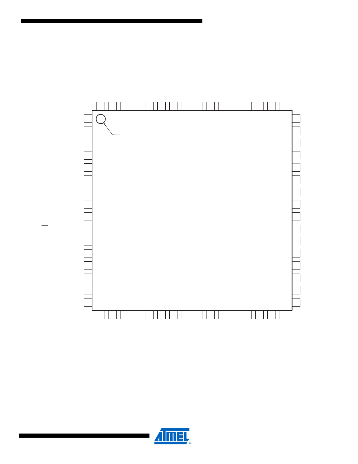
Figure 1-2.
Pinout ATmega329/649
Note:
The large center pad underneath the QFN/MLF packages is made of metal and internally con-
nected to GND. It should be soldered or glued to the board to ensure good mechanical stability. If
the center pad is left unconnected, the package might loosen from the board.
PC0 (SEG12)
V
CC
GND
PF0 (ADC0)
PF7 (ADC7/TDI)
PF1 (ADC1)
PF2 (ADC2)
PF3 (ADC3)
PF4 (ADC4/TCK)
PF5 (ADC5/TMS)
PF6 (ADC6/TDO)
AREF
GND
A
V
CC
17
61
60
18
59
20
58
19
21
57
22
56
23
55
24
54
25
53
26
52
27
51
29
28
50
49
32
31
30
(RXD/PCINT0) PE0
(TXD/PCINT1) PE1
LCDCAP
(XCK/AIN0/PCINT2) PE2
(AIN1/PCINT3) PE3
(USCK/SCL/PCINT4) PE4
(DI/SDA/PCINT5) PE5
(DO/PCINT6) PE6
(CLKO/PCINT7) PE7
(SCK/PCINT9) PB1
(MOSI/PCINT10) PB2
(MISO/PCINT11) PB3
(OC0A/PCINT12) PB4
(OC2A/PCINT15) PB7
(T1/SEG24) PG3
(OC1B/PCINT14) PB6
(T0/SEG23) PG4
(OC1A/PCINT13) PB5
PC1 (SEG11)
PG0 (SEG14)
(SEG15) PD7
PC2 (SEG10)
PC3 (SEG9)
PC4 (SEG8)
PC5 (SEG7)
PC6 (SEG6)
PC7 (SEG5)
PA7 (SEG3)
PG2 (SEG4)
PA6 (SEG2)
PA5 (SEG1)
PA4 (SEG0)
PA3 (COM3)
PA0 (COM0)
PA1 (COM1)
PA2 (COM2)
PG1 (SEG13)
(SEG16) PD6
(SEG17) PD5
(SEG18) PD4
(SEG19) PD3
(SEG20) PD2
(INT0/SEG21) PD1
(ICP1/SEG22) PD0
(TOSC1) XTAL1
(TOSC2) XTAL2
RESET/PG5
GND
V
CC
INDEX CORNER
(SS/PCINT8) PB0
2
3
1
4
5
6
7
8
9
10
11
12
13
14
16
15
64
63
62
47
46
48
45
44
43
42
41
40
39
38
37
36
35
33
34
ATmega329/649
4
2552KS–AVR–04/11
ATmega329/3290/649/6490
2.
Overview
The ATmega329/3290/649/6490 is a low-power CMOS 8-bit microcontroller based on the AVR enhanced RISC architec-
ture. By executing powerful instructions in a single clock cycle, the ATmega329/3290/649/6490 achieves throughputs
approaching 1 MIPS per MHz allowing the system designer to optimize power consumption versus processing speed.
2.1
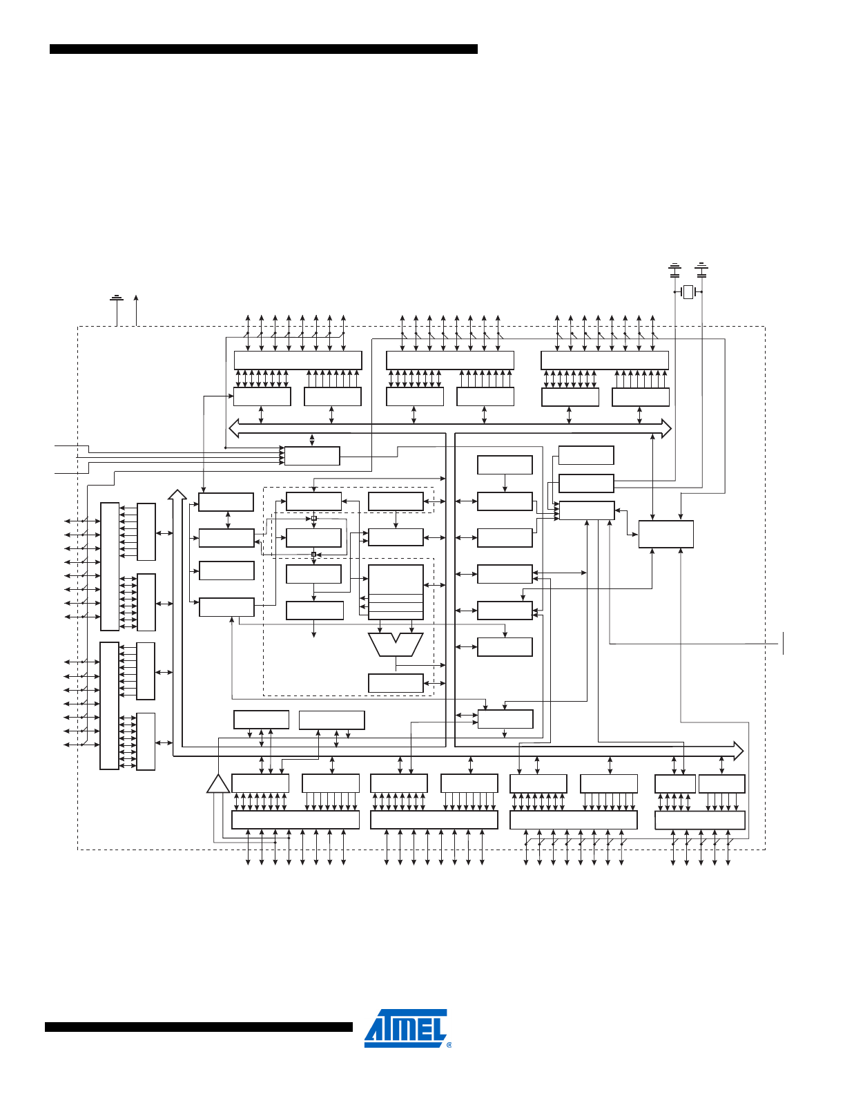
Block Diagram
Figure 2-1.
Block Diagram
PROGRAM
COUNTER
INTERNAL
OSCILLATOR
WATCHDOG
TIMER
STACK
POINTER
PROGRAM
FLASH
MCU CONTROL
REGISTER
SRAM
GENERAL
PURPOSE
REGISTERS
INSTRUCTION
REGISTER
TIMER/
COUNTERS
INSTRUCTION
DECODER
DATA DIR.
REG. PORTB
DATA DIR.
REG. PORTE
DATA DIR.
REG. PORTA
DATA DIR.
REG. PORTD
DATA REGISTER
PORTB
DATA REGISTER
PORTE
DATA REGISTER
PORTA
DATA REGISTER
PORTD
TIMING AND
CONTROL
OSCILLATOR
INTERRUPT
UNIT
EEPROM
SPI
USART
STATUS
REGISTER
Z
Y
X
ALU
PORTB DRIVERS
PORTE DRIVERS
PORTA DRIVERS
PORTF DRIVERS
PORTD DRIVERS
PORTC DRIVERS
PB0 - PB7
PE0 - PE7
PA0 - PA7
PF0 - PF7
VCC
GND
XT
AL1
XT
AL2
CONTROL
LINES
+
-
ANALOG
COMP
ARA
T
O
R
PC0 - PC7
8-BIT DATA BUS
RESET
CALIB. OSC
DATA DIR.
REG. PORTC
DATA REGISTER
PORTC
ON-CHIP DEBUG
JTAG TAP
PROGRAMMING
LOGIC
BOUNDARY-
SCAN
DATA DIR.
REG. PORTF
DATA REGISTER
PORTF
ADC
PD0 - PD7
DATA DIR.
REG. PORTG
DATA REG.
PORTG
PORTG DRIVERS
PG0 - PG4
AGND
AREF
AVCC
UNIVERSAL
SERIAL INTERFACE
AVR CPU
LCD
CONTROLLER/
DRIVER
POR
TH DRIVERS
PH0 - PH7
D
A
T
A
DIR.
REG.
POR
T
H
D
A
T
A
REGISTER
POR
T
H
POR
TJ DRIVERS
PJ0 - PJ6
D
A
T
A
DIR.
REG.
POR
T
J
D
A
T
A
REGISTER
POR
T
J

5
2552KS–AVR–04/11
ATmega329/3290/649/6490
The Atmel
®
AVR
®
core combines a rich instruction set with 32 general purpose working regis-
ters. All the 32 registers are directly connected to the Arithmetic Logic Unit (ALU), allowing two
independent registers to be accessed in one single instruction executed in one clock cycle. The
resulting architecture is more code efficient while achieving throughputs up to ten times faster
than conventional CISC microcontrollers.
The Atmel ATmega329/3290/649/6490 provides the following features: 32/64K bytes of In-Sys-
tem Programmable Flash with Read-While-Write capabilities, 1/2K bytes EEPROM, 2/4K byte
SRAM, 54/69 general purpose I/O lines, 32 general purpose working registers, a JTAG interface
for Boundary-scan, On-chip Debugging support and programming, a complete On-chip LCD
controller with internal contrast control, three flexible Timer/Counters with compare modes, inter-
nal and external interrupts, a serial programmable USART, Universal Serial Interface with Start
Condition Detector, an 8-channel, 10-bit ADC, a programmable Watchdog Timer with internal
Oscillator, an SPI serial port, and five software selectable power saving modes. The Idle mode
stops the CPU while allowing the SRAM, Timer/Counters, SPI port, and interrupt system to con-
tinue functioning. The Power-down mode saves the register contents but freezes the Oscillator,
disabling all other chip functions until the next interrupt or hardware reset. In Power-save mode,
the asynchronous timer and the LCD controller continues to run, allowing the user to maintain a
timer base and operate the LCD display while the rest of the device is sleeping. The ADC Noise
Reduction mode stops the CPU and all I/O modules except asynchronous timer, LCD controller
and ADC, to minimize switching noise during ADC conversions. In Standby mode, the crys-
tal/resonator Oscillator is running while the rest of the device is sleeping. This allows very fast
start-up combined with low-power consumption.
The device is manufactured using Atmel’s high density non-volatile memory technology. The
On-chip In-System re-Programmable (ISP) Flash allows the program memory to be repro-
grammed In-System through an SPI serial interface, by a conventional non-volatile memory
programmer, or by an On-chip Boot program running on the AVR core. The Boot program can
use any interface to download the application program in the Application Flash memory. Soft-
ware in the Boot Flash section will continue to run while the Application Flash section is updated,
providing true Read-While-Write operation. By combining an 8-bit RISC CPU with In-System
Self-Programmable Flash on a monolithic chip, the Atmel ATmega329/3290/649/6490 is a pow-
erful microcontroller that provides a highly flexible and cost effective solution to many embedded
control applications.
The Atmel ATmega329/3290/649/6490 is supported with a full suite of program and system
development tools including: C Compilers, Macro Assemblers, Program Debugger/Simulators,
In-Circuit Emulators, and Evaluation kits.
6
2552KS–AVR–04/11
ATmega329/3290/649/6490
2.2
Comparison between ATmega329, ATmega3290, ATmega649 and ATmega6490
The ATmega329, ATmega3290, ATmega649, and ATmega6490 differs only in memory sizes,
pin count and pinout.
Table 2-1 on page 6
summarizes the different configurations for the four
devices.
2.3
Pin Descriptions
The following section describes the I/O-pin special functions.
2.3.1
V
CC
Digital supply voltage.
2.3.2
GND
Ground.
2.3.3
Port A (PA7..PA0)
Port A is an 8-bit bi-directional I/O port with internal pull-up resistors (selected for each bit). The
Port A output buffers have symmetrical drive characteristics with both high sink and source
capability. As inputs, Port A pins that are externally pulled low will source current if the pull-up
resistors are activated. The Port A pins are tri-stated when a reset condition becomes active,
even if the clock is not running.
Port A also serves the functions of various special features of the ATmega329/3290/649/6490
as listed on
page 67
.
2.3.4
Port B (PB7..PB0)
Port B is an 8-bit bi-directional I/O port with internal pull-up resistors (selected for each bit). The
Port B output buffers have symmetrical drive characteristics with both high sink and source
capability. As inputs, Port B pins that are externally pulled low will source current if the pull-up
resistors are activated. The Port B pins are tri-stated when a reset condition becomes active,
even if the clock is not running.
Port B has better driving capabilities than the other ports.
Port B also serves the functions of various special features of the ATmega329/3290/649/6490
as listed on
page 68
.
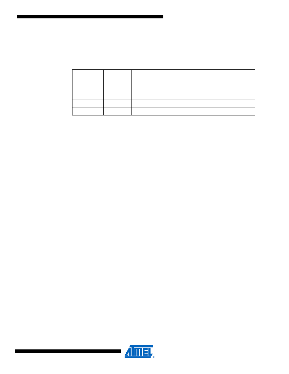
Table 2-1.
Configuration Summary
Device
Flash
EEPROM
RAM
LCD
Segments
General Purpose
I/O Pins
ATmega329
32Kbytes
1Kbytes
2Kbytes
4 x 25
54
ATmega3290
32Kbytes
1K bytes
2Kbytes
4 x 40
69
ATmega649
64Kbytes
2Kbytes
4Kbytes
4 x 25
54
ATmega6490
64Kbytes
2Kbytes
4Kbytes
4 x 40
69

7
2552KS–AVR–04/11
ATmega329/3290/649/6490
2.3.5
Port C (PC7..PC0)
Port C is an 8-bit bi-directional I/O port with internal pull-up resistors (selected for each bit). The
Port C output buffers have symmetrical drive characteristics with both high sink and source
capability. As inputs, Port C pins that are externally pulled low will source current if the pull-up
resistors are activated. The Port C pins are tri-stated when a reset condition becomes active,
even if the clock is not running.
Port C also serves the functions of special features of the ATmega329/3290/649/6490 as listed
on
page 71
.
2.3.6
Port D (PD7..PD0)
Port D is an 8-bit bi-directional I/O port with internal pull-up resistors (selected for each bit). The
Port D output buffers have symmetrical drive characteristics with both high sink and source
capability. As inputs, Port D pins that are externally pulled low will source current if the pull-up
resistors are activated. The Port D pins are tri-stated when a reset condition becomes active,
even if the clock is not running.
Port D also serves the functions of various special features of the ATmega329/3290/649/6490
as listed on
page 73
.
2.3.7
Port E (PE7..PE0)
Port E is an 8-bit bi-directional I/O port with internal pull-up resistors (selected for each bit). The
Port E output buffers have symmetrical drive characteristics with both high sink and source
capability. As inputs, Port E pins that are externally pulled low will source current if the pull-up
resistors are activated. The Port E pins are tri-stated when a reset condition becomes active,
even if the clock is not running.
Port E also serves the functions of various special features of the ATmega329/3290/649/6490
as listed on
page 75
.
2.3.8
Port F (PF7..PF0)
Port F serves as the analog inputs to the A/D Converter.
Port F also serves as an 8-bit bi-directional I/O port, if the A/D Converter is not used. Port pins
can provide internal pull-up resistors (selected for each bit). The Port F output buffers have sym-
metrical drive characteristics with both high sink and source capability. As inputs, Port F pins
that are externally pulled low will source current if the pull-up resistors are activated. The Port F
pins are tri-stated when a reset condition becomes active, even if the clock is not running. If the
JTAG interface is enabled, the pull-up resistors on pins PF7(TDI), PF5(TMS), and PF4(TCK) will
be activated even if a reset occurs.
Port F also serves the functions of the JTAG interface.

8
2552KS–AVR–04/11
ATmega329/3290/649/6490
2.3.9
Port G (PG5..PG0)
Port G is a 6-bit bi-directional I/O port with internal pull-up resistors (selected for each bit). The
Port G output buffers have symmetrical drive characteristics with both high sink and source
capability. As inputs, Port G pins that are externally pulled low will source current if the pull-up
resistors are activated. The Port G pins are tri-stated when a reset condition becomes active,
even if the clock is not running.
Port G also serves the functions of various special features of the ATmega329/3290/649/6490
as listed on
page 75
.
2.3.10
Port H (PH7..PH0)
Port H is a 8-bit bi-directional I/O port with internal pull-up resistors (selected for each bit). The
Port H output buffers have symmetrical drive characteristics with both high sink and source
capability. As inputs, Port H pins that are externally pulled low will source current if the pull-up
resistors are activated. The Port H pins are tri-stated when a reset condition becomes active,
even if the clock is not running.
Port H also serves the functions of various special features of the ATmega3290/6490 as listed
on
page 75
.
2.3.11
Port J (PJ6..PJ0)
Port J is a 7-bit bi-directional I/O port with internal pull-up resistors (selected for each bit). The
Port J output buffers have symmetrical drive characteristics with both high sink and source capa-
bility. As inputs, Port J pins that are externally pulled low will source current if the pull-up
resistors are activated. The Port J pins are tri-stated when a reset condition becomes active,
even if the clock is not running.
Port J also serves the functions of various special features of the ATmega3290/6490 as listed on
page 75
.
2.3.12
RESET
Reset input. A low level on this pin for longer than the minimum pulse length will generate a
reset, even if the clock is not running. The minimum pulse length is given in
“System and Reset
Characteristics” on page 330
. Shorter pulses are not guaranteed to generate a reset.
2.3.13
XTAL1
Input to the inverting Oscillator amplifier and input to the internal clock operating circuit.
2.3.14
XTAL2
Output from the inverting Oscillator amplifier.
2.3.15
AVCC
AVCC is the supply voltage pin for Port F and the A/D Converter. It should be externally con-
nected to V
CC
, even if the ADC is not used. If the ADC is used, it should be connected to V
CC
through a low-pass filter.
2.3.16
AREF
This is the analog reference pin for the A/D Converter.

9
2552KS–AVR–04/11
ATmega329/3290/649/6490
2.3.17
LCDCAP
An external capacitor (typical > 470nF) must be connected to the LCDCAP pin as shown in
Fig-
ure 23-2
. This capacitor acts as a reservoir for LCD power (V
LCD
). A large capacitance reduces
ripple on V
LCD
but increases the time until V
LCD
reaches its target value.
3.
Resources
A comprehensive set of development tools, application notes and datasheets are available for
download on http://www.atmel.com/avr.
Note:
1.
4.
Data Retention
Reliability Qualification results show that the projected data retention failure rate is much less
than 1 PPM over 20 years at 85°C or 100 years at 25°C.
5.
About Code Examples
This documentation contains simple code examples that briefly show how to use various parts of
the device. These code examples assume that the part specific header file is included before
compilation. Be aware that not all C compiler vendors include bit definitions in the header files
and interrupt handling in C is compiler dependent. Please confirm with the C compiler documen-
tation for more details.
For I/O Registers located in extended I/O map, “IN”, “OUT”, “SBIS”, “SBIC”, “CBI”, and “SBI”
instructions must be replaced with instructions that allow access to extended I/O. Typically
“LDS” and “STS” combined with “SBRS”, “SBRC”, “SBR”, and “CBR”.
10
2552KS–AVR–04/11
ATmega329/3290/649/6490
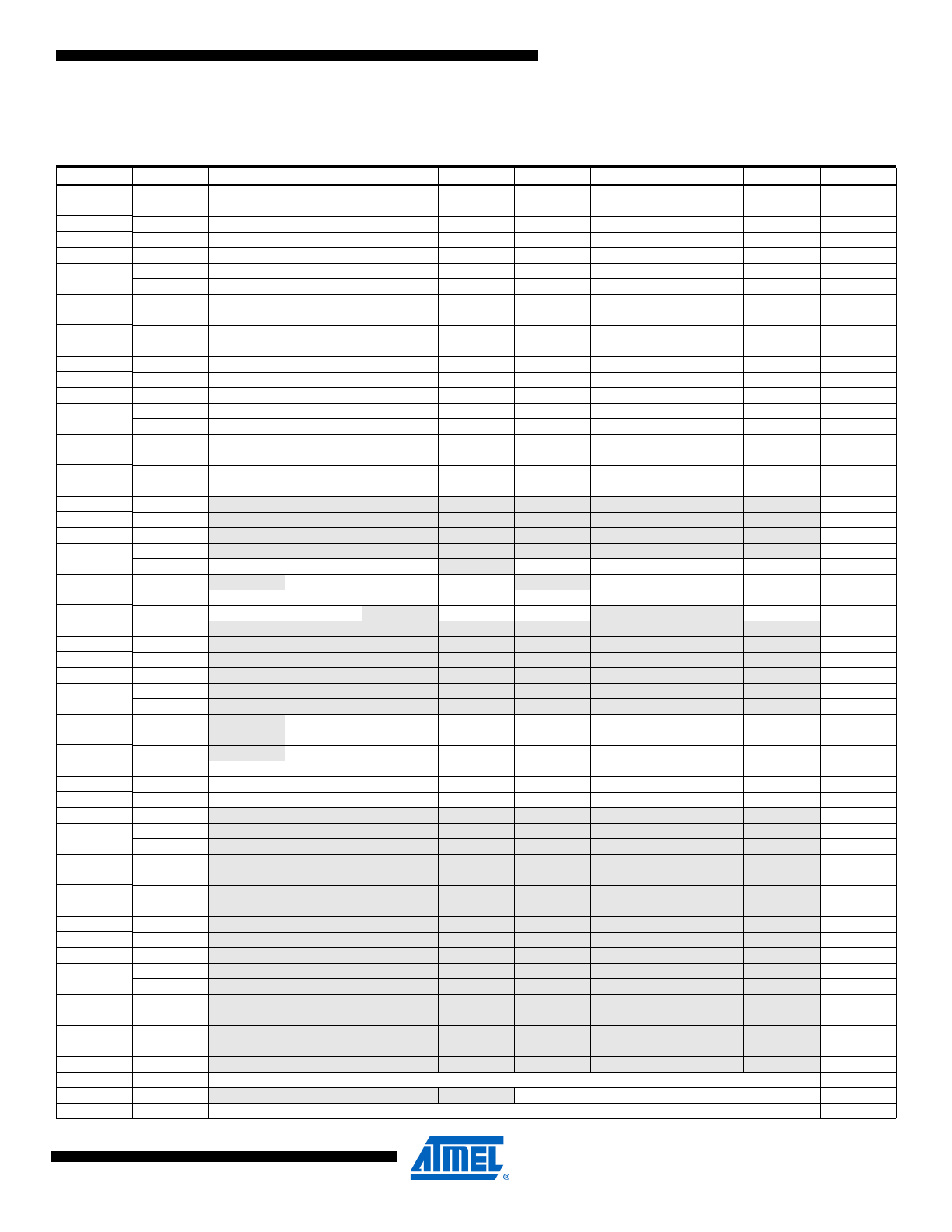
6.
Register Summary
Note:
Registers with bold type only available in ATmega3290/6490.
Address
Name
Bit 7
Bit 6
Bit 5
Bit 4
Bit 3
Bit 2
Bit 1
Bit 0
Page
(0xFF)
LCDDR19
SEG339
SEG338
SEG337
SEG336
SEG335
SEG334
SEG333
SEG332
244
(0xFE)
LCDDR18
SEG331
SEG330
SEG329
SEG328
SEG327
SEG326
SEG325
SEG324
244
(0xFD)
LCDDR17
SEG323
SEG322
SEG321
SEG320
SEG319
SEG318
SEG317
SEG316
244
(0xFC)
LCDDR16
SEG315
SEG314
SEG313
SEG312
SEG311
SEG310
SEG309
SEG308
244
(0xFB)
LCDDR15
SEG307
SEG306
SEG305
SEG304
SEG303
SEG302
SEG301
SEG300
244
(0xFA)
LCDDR14
SEG239
SEG238
SEG237
SEG236
SEG235
SEG234
SEG233
SEG232
244
(0xF9)
LCDDR13
SEG231
SEG230
SEG229
SEG228
SEG227
SEG226
SEG225
SEG224
244
(0xF8)
LCDDR12
SEG223
SEG222
SEG221
SEG220
SEG219
SEG218
SEG217
SEG216
244
(0xF7)
LCDDR11
SEG215
SEG214
SEG213
SEG212
SEG211
SEG210
SEG209
SEG208
244
(0xF6)
LCDDR10
SEG207
SEG206
SEG205
SEG204
SEG203
SEG202
SEG201
SEG200
244
(0xF5)
LCDDR09
SEG139
SEG138
SEG137
SEG136
SEG135
SEG134
SEG133
SEG132
244
(0xF4)
LCDDR08
SEG131
SEG130
SEG129
SEG128
SEG127
SEG126
SEG125
SEG124
244
(0xF3)
LCDDR07
SEG123
SEG122
SEG121
SEG120
SEG119
SEG118
SEG117
SEG116
244
(0xF2)
LCDDR06
SEG115
SEG114
SEG113
SEG112
SEG111
SEG110
SEG109
SEG108
244
(0xF1)
LCDDR05
SEG107
SEG106
SEG105
SEG104
SEG103
SEG102
SEG101
SEG100
244
(0xF0)
LCDDR04
SEG039
SEG038
SEG037
SEG036
SEG035
SEG034
SEG033
SEG032
244
(0xEF)
LCDDR03
SEG031
SEG030
SEG029
SEG028
SEG027
SEG026
SEG025
SEG024
244
(0xEE)
LCDDR02
SEG023
SEG022
SEG021
SEG020
SEG019
SEG018
SEG017
SEG016
244
(0xED)
LCDDR01
SEG015
SEG014
SEG013
SEG012
SEG011
SEG010
SEG009
SEG008
244
(0xEC)
LCDDR00
SEG007
SEG006
SEG005
SEG004
SEG003
SEG002
SEG001
SEG000
244
(0xEB)
Reserved
-
-
-
-
-
-
-
-
(0xEA)
Reserved
-
-
-
-
-
-
-
-
(0xE9)
Reserved
-
-
-
-
-
-
-
-
(0xE8)
Reserved
-
-
-
-
-
-
-
-
(0xE7)
LCDCCR
LCDDC2
LCDDC1
LCDDC0
-
LCDCC3 LCDCC2
LCDCC1
LCDCC0
243
(0xE6)
LCDFRR
-
LCDPS2 LCDPS1
LCDPS0
-
LCDCD2
LCDCD1
LCDCD0
241
(0xE5)
LCDCRB
LCDCS LCD2B
LCDMUX1
LCDMUX0
LCDPM3
LCDPM2
LCDPM1
LCDPM0
239
(0xE4)
LCDCRA
LCDEN LCDAB
-
LCDIF
LCDIE
-
-
LCDBL
239
(0xE3)
Reserved
-
-
-
-
-
-
-
-
(0xE2)
Reserved
-
-
-
-
-
-
-
-
(0xE1)
Reserved
-
-
-
-
-
-
-
-
(0xE0)
Reserved
-
-
-
-
-
-
-
-
(0xDF)
Reserved
-
-
-
-
-
-
-
-
(0xDE)
Reserved
-
-
-
-
-
-
-
-
(0xDD)
PORTJ
-
PORTJ6
PORTJ5
PORTJ4
PORTJ3
PORTJ2
PORTJ1
PORTJ0
90
(0xDC)
DDRJ
-
DDJ6
DDJ5
DDJ4
DDJ3
DDJ2
DDJ1
DDJ0
90
(0xDB)
PINJ
-
PINJ6
PINJ5
PINJ4
PINJ3
PINJ2
PINJ1
PINJ0
90
(0xDA)
PORTH
PORTH7
PORTH6
PORTH5
PORTH4
PORTH3
PORTH2
PORTH1
PORTH0
89
(0xD9)
DDRH
DDH7
DDH6
DDH5
DDH4
DDH3
DDH2
DDH1
DDH0
90
(0xD8)
PINH
PINH7
PINH6
PINH5
PINH4
PINH3
PINH2
PINH1
PINH0
90
(0xD7)
Reserved
-
-
-
-
-
-
-
-
(0xD6)
Reserved
-
-
-
-
-
-
-
-
(0xD5)
Reserved
-
-
-
-
-
-
-
-
(0xD4)
Reserved
-
-
-
-
-
-
-
-
(0xD3)
Reserved
-
-
-
-
-
-
-
-
(0xD2)
Reserved
-
-
-
-
-
-
-
-
(0xD1)
Reserved
-
-
-
-
-
-
-
-
(0xD0)
Reserved
-
-
-
-
-
-
-
-
(0xCF)
Reserved
-
-
-
-
-
-
-
-
(0xCE)
Reserved
-
-
-
-
-
-
-
-
(0xCD)
Reserved
-
-
-
-
-
-
-
-
(0xCC)
Reserved
-
-
-
-
-
-
-
-
(0xCB)
Reserved
-
-
-
-
-
-
-
-
(0xCA)
Reserved
-
-
-
-
-
-
-
-
(0xC9)
Reserved
-
-
-
-
-
-
-
-
(0xC8)
Reserved
-
-
-
-
-
-
-
-
(0xC7)
Reserved
-
-
-
-
-
-
-
-
(0xC6)
UDR0
USART0 Data Register
190
(0xC5)
UBRR0H
USART0 Baud Rate Register High
194
(0xC4)
UBRR0L
USART0 Baud Rate Register Low
194