

Features
•
High Performance, Low Power AVR
®
8-Bit Microcontroller
•
Advanced RISC Architecture
– 130 Powerful Instructions – Most Single Clock Cycle Execution
– 32 x 8 General Purpose Working Registers
– Fully Static Operation
– Up to 20 MIPS Throughput at 20 MHz
– On-Chip 2-cycle Multiplier
•
High Endurance Non-volatile Memory segments
– 32K Bytes of In-System Self-programmable Flash program memory
– 1K Bytes EEPROM
– 2K Bytes Internal SRAM
– Write/Erase cyles: 10,000 Flash/100,000 EEPROM
– Data retention: 20 years at 85°C/100 years at 25°C
(1)
– Optional Boot Code Section with Independent Lock Bits
In-System Programming by On-chip Boot Program
True Read-While-Write Operation
– Programming Lock for Software Security
•
JTAG (IEEE std. 1149.1 compliant) Interface
– Boundary-scan Capabilities According to the JTAG Standard
– Extensive On-chip Debug Support
– Programming of Flash, EEPROM, Fuses, and Lock Bits through the JTAG Interface
•
Peripheral Features
– Two 8-bit Timer/Counters with Separate Prescaler and Compare Mode
– One 16-bit Timer/Counter with Separate Prescaler, Compare Mode, and Capture
Mode
– Real Time Counter with Separate Oscillator
– Four PWM Channels
– 8-channel, 10-bit ADC
– Programmable Serial USART
– Master/Slave SPI Serial Interface
– Universal Serial Interface with Start Condition Detector
– Programmable Watchdog Timer with Separate On-chip Oscillator
– On-chip Analog Comparator
– Interrupt and Wake-up on Pin Change
•
Special Microcontroller Features
– Power-on Reset and Programmable Brown-out Detection
– Internal Calibrated Oscillator
– External and Internal Interrupt Sources
– Five Sleep Modes: Idle, ADC Noise Reduction, Power-save, Power-down, and
Standby
•
I/O and Packages
– 54/69 Programmable I/O Lines
– 64-lead TQFP, 64-pad QFN/MLF, and 100-lead TQFP
•
Speed Grade:
– ATmega325PV/ATmega3250PV:
0 - 4 MHz @ 1.8 - 5.5V, 0 - 10 MHz @ 2.7 - 5.5V
– ATmega325P/3250P:
0 - 10 MHz @ 2.7 - 5.5V, 0 - 20 MHz @ 4.5 - 5.5V
•
Temperature range:
– -40°C to 85°C Industrial
•
Ultra-Low Power Consumption
– Active Mode:
420 µA at 1 MHz, 1.8V
– Power-down Mode:
40 nA at 1.8V
– Power-save Mode:
750 nA at 1.8V
8-bit
Microcontroller
with 32K Bytes
In-System
Programmable
Flash
ATmega325P/V
ATmega3250P/V
Preliminary
8023FS–AVR–07/09
2
8023FS–AVR–07/09
ATmega325P/3250P
1.
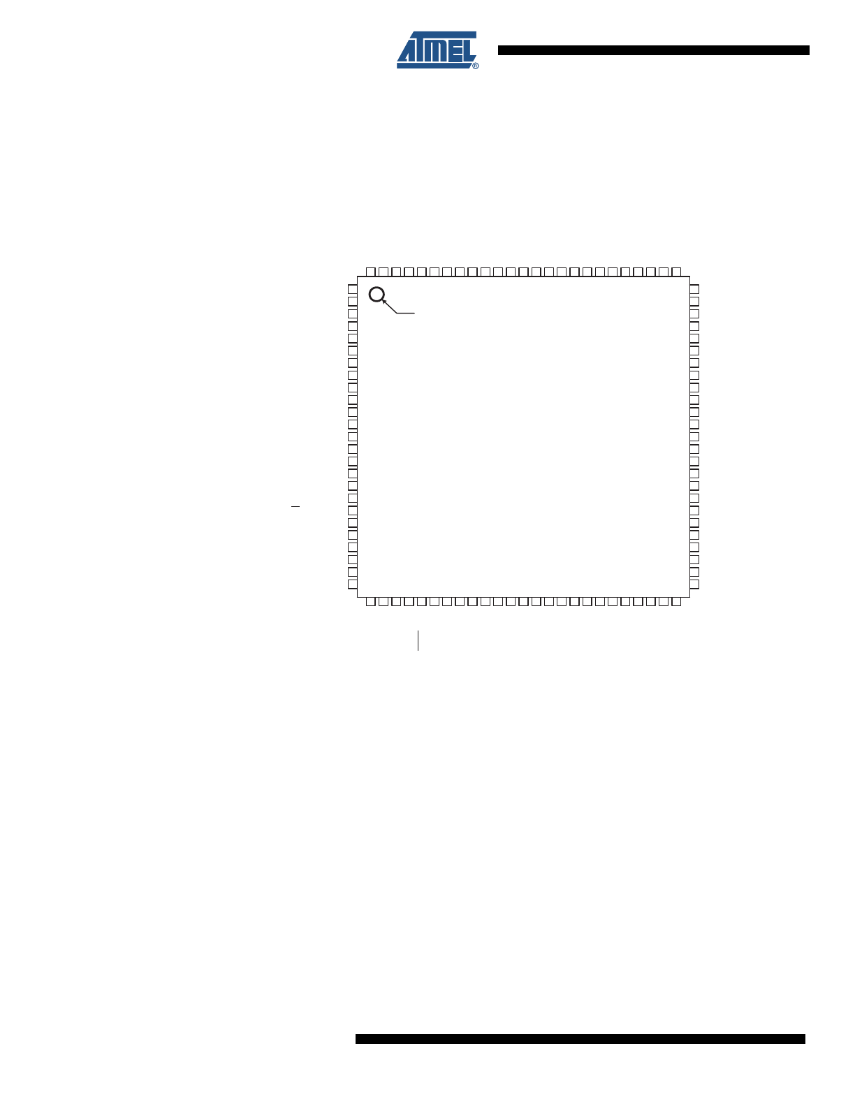
Pin Configurations
Figure 1-1.
Pinout ATmega3250P
(OC2A/PCINT15) PB7
DNC
(T1) PG3
(T0) PG4
RESET/PG5
VCC
GND
(T
OSC2) XT
AL2
(T
OSC1) XT
AL1
DNC
DNC
(PCINT26) PJ2
(PCINT27) PJ3
(PCINT28) PJ4
(PCINT29) PJ5
(PCINT30) PJ6
DNC
(ICP1) PD0
(INT0) PD1
PD2
PD3
PD4
PD5
PD6
PD7
AV
C
C
AG
N
D
AREF
PF0 (ADC0)
PF1 (ADC1)
PF2 (ADC2)
PF3 (ADC3)
PF4 (ADC4/TCK)
PF5 (ADC5/TMS)
PF6 (ADC6/TDO)
PF7 (ADC7/TDI)
DNC
DNC
PH7 (PCINT23)
PH6 (PCINT22)
PH5 (PCINT21)
PH4 (PCINT20)
DNC
DNC
GND
VCC
DNC
PA
0
PA
1
PA
2
PA3
PA4
PA5
PA6
PA7
PG2
PC7
PC6
DNC
PH3 (PCINT19)
PH2 (PCINT18)
PH1 (PCINT17)
PH0 (PCINT16)
DNC
DNC
DNC
DNC
PC5
PC4
PC3
PC2
PC1
PC0
PG1
PG0
INDEX CORNER
ATmega3250
1
2
3
4
5
6
7
8
9
10
11
12
13
14
15
16
17
18
19
20
21
22
23
24
25
26
27
28
29
30
31
32
33
34
35
36
37
38
39
40
41
42
43
44
45
46
47
48
49
50
75
74
73
72
71
70
69
68
67
66
65
64
63
62
61
60
59
58
57
56
55
54
53
52
51
100
99
98
97
96
95
94
93
92
91
90
89
88
87
86
85
84
83
82
81
80
79
78
77
76
DNC
(RXD/PCINT0) PE0
(TXD/PCINT1) PE1
(XCK/AIN0/PCINT2) PE2
(AIN1/PCINT3) PE3
(USCK/SCL/PCINT4) PE4
(DI/SDA/PCINT5) PE5
(DO/PCINT6) PE6
(CLKO/PCINT7) PE7
VCC
GND
DNC
(PCINT24) PJ0
(PCINT25) PJ1
DNC
DNC
DNC
DNC
(SS/PCINT8) PB0
(SCK/PCINT9) PB1
(MOSI/PCINT10) PB2
(MISO/PCINT11) PB3
(OC0A/PCINT12) PB4
(OC1A/PCINT13) PB5
(OC1B/PCINT14) PB6
TQFP
3
8023FS–AVR–07/09
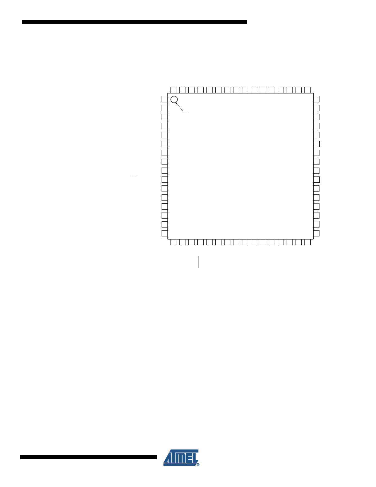
ATmega325P/3250P
Figure 1-2.
Pinout ATmega325P
Note:
The large center pad underneath the QFN/MLF packages is made of metal and internally con-
nected to GND. It should be soldered or glued to the board to ensure good mechanical stability. If
the center pad is left unconnected, the package might loosen from the board.
1.1
Disclaimer
Typical values contained in this datasheet are based on simulations and characterization of
other AVR microcontrollers manufactured on the same process technology. Min and Max values
will be available after the device is characterized.
2.
Overview
The ATmega325P/3250P is a low-power CMOS 8-bit microcontroller based on the AVR enhanced RISC architecture. By
executing powerful instructions in a single clock cycle, the ATmega325P/3250P achieves throughputs approaching 1 MIPS
per MHz allowing the system designer to optimize power consumption versus processing speed.
PC0
VCC
GND
PF0 (ADC0)
PF7 (ADC7/TDI)
PF1 (ADC1)
PF2 (ADC2)
PF3 (ADC3)
PF4 (ADC4/TCK)
PF5 (ADC5/TMS)
PF6 (ADC6/TDO)
AREF
GND
A
VCC
17
61
60
18
59
20
58
19
21
57
22
56
23
55
24
54
25
53
26
52
27
51
29
28
50
49
32
31
30
(RXD/PCINT0) PE0
(TXD/PCINT1) PE1
DNC
(XCK/AIN0/PCINT2) PE2
(AIN1/PCINT3) PE3
(USCK/SCL/PCINT4) PE4
(DI/SDA/PCINT5) PE5
(DO/PCINT6) PE6
(CLKO/PCINT7) PE7
(SCK/PCINT9) PB1
(MOSI/PCINT10) PB2
(MISO/PCINT11) PB3
(OC0A/PCINT12) PB4
(OC2A/PCINT15) PB7
(T1) PG3
(OC1B/PCINT14) PB6
(T0) PG4
(OC1A/PCINT13) PB5
PC1
PG0
PD7
PC2
PC3
PC4
PC5
PC6
PC7
PA7
PG2
PA6
PA5
PA4
PA3
PA
0
PA
1
PA
2
PG1
PD6
PD5
PD4
PD3
PD2
(INT0) PD1
(ICP1) PD0
(T
OSC1) XT
AL1
(T
OSC2) XT
AL2
RESET/PG5
GND
VCC
INDEX CORNER
(SS/PCINT8) PB0
2
3
1
4
5
6
7
8
9
10
11
12
13
14
16
15
64
63
62
47
46
48
45
44
43
42
41
40
39
38
37
36
35
33
34
ATmega325
4
8023FS–AVR–07/09
ATmega325P/3250P
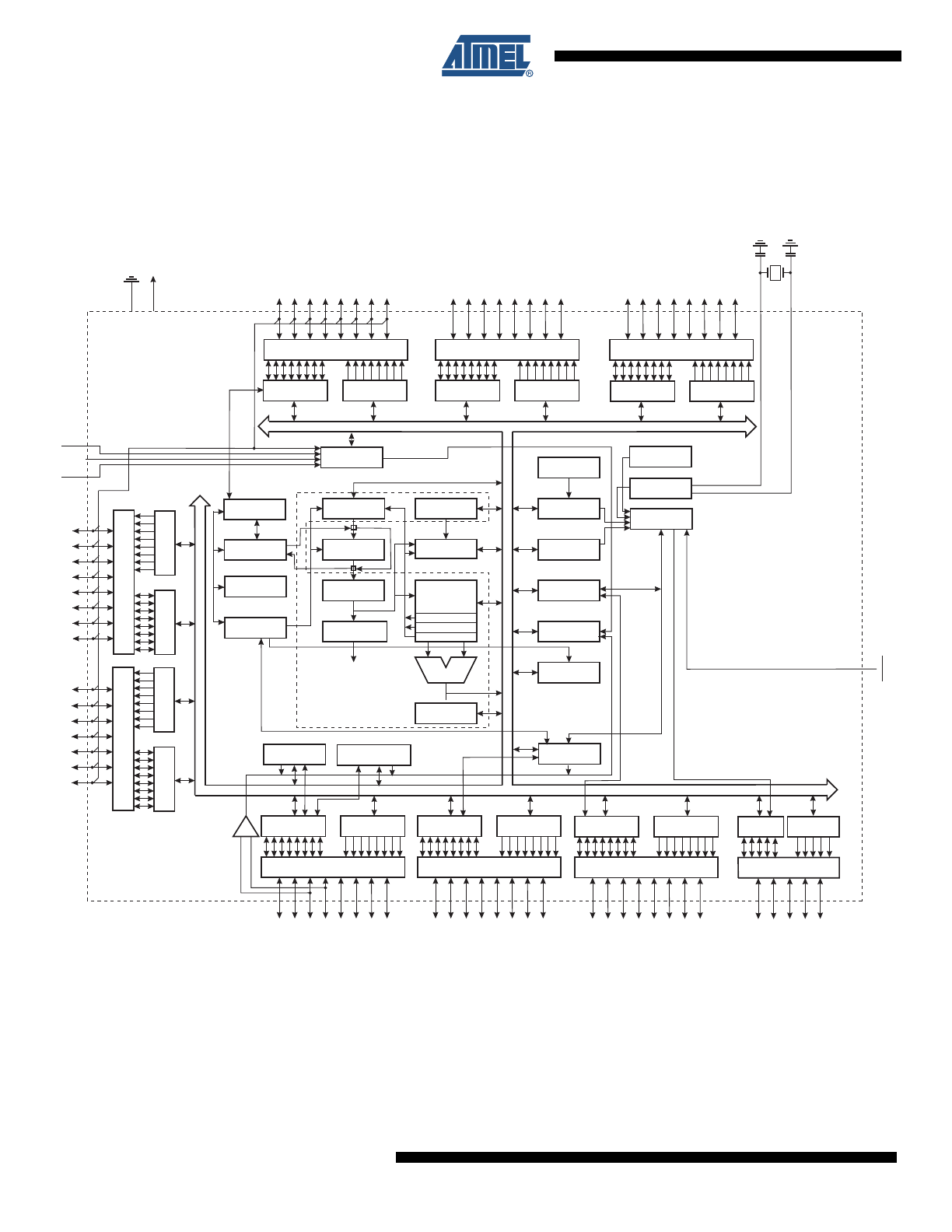
2.1
Block Diagram
Figure 2-1.
Block Diagram
The AVR core combines a rich instruction set with 32 general purpose working registers. All the
32 registers are directly connected to the Arithmetic Logic Unit (ALU), allowing two independent
registers to be accessed in one single instruction executed in one clock cycle. The resulting
architecture is more code efficient while achieving throughputs up to ten times faster than con-
ventional CISC microcontrollers.
PROGRAM
COUNTER
INTERNAL
OSCILLATOR
WATCHDOG
TIMER
STACK
POINTER
PROGRAM
FLASH
MCU CONTROL
REGISTER
SRAM
GENERAL
PURPOSE
REGISTERS
INSTRUCTION
REGISTER
TIMER/
COUNTERS
INSTRUCTION
DECODER
DATA DIR.
REG. PORTB
DATA DIR.
REG. PORTE
DATA DIR.
REG. PORTA
DATA DIR.
REG. PORTD
DATA REGISTER
PORTB
DATA REGISTER
PORTE
DATA REGISTER
PORTA
DATA REGISTER
PORTD
TIMING AND
CONTROL
OSCILLATOR
INTERRUPT
UNIT
EEPROM
SPI
USART
STATUS
REGISTER
Z
Y
X
ALU
PORTB DRIVERS
PORTE DRIVERS
PORTA DRIVERS
PORTF DRIVERS
PORTD DRIVERS
PORTC DRIVERS
PB0 - PB7
PE0 - PE7
PA0 - PA7
PF0 - PF7
VCC
GND
XT
AL1
XT
AL2
CONTROL
LINES
+
-
A
N
ALOG
COMP
ARA
T
O
R
PC0 - PC7
8-BIT DATA BUS
RESET
CALIB. OSC
DATA DIR.
REG. PORTC
DATA REGISTER
PORTC
ON-CHIP DEBUG
JTAG TAP
PROGRAMMING
LOGIC
BOUNDARY-
SCAN
DATA DIR.
REG. PORTF
DATA REGISTER
PORTF
ADC
PD0 - PD7
DATA DIR.
REG. PORTG
DATA REG.
PORTG
PORTG DRIVERS
PG0 - PG4
AGND
AREF
AVCC
UNIVERSAL
SERIAL INTERFACE
AVR CPU
POR
TH DRI
V
ERS
PH0 - PH7
D
A
T
A
DIR.
REG.
POR
T
H
D
A
T
A
REGISTER
POR
T
H
POR
TJ DRI
V
ERS
PJ0 - PJ6
D
A
T
A
DIR.
REG.
POR
T
J
D
A
T
A
REGISTER
POR
T
J

5
8023FS–AVR–07/09
ATmega325P/3250P
The ATmega325P/3250P provides the following features: 32K bytes of In-System Programma-
ble Flash with Read-While-Write capabilities, 1K bytes EEPROM, 2K byte SRAM, 54/69 general
purpose I/O lines, 32 general purpose working registers, a JTAG interface for Boundary-scan,
On-chip Debugging support and programming, three flexible Timer/Counters with compare
modes, internal and external interrupts, a serial programmable USART, Universal Serial Inter-
face with Start Condition Detector, an 8-channel, 10-bit ADC, a programmable Watchdog Timer
with internal Oscillator, an SPI serial port, and five software selectable power saving modes. The
Idle mode stops the CPU while allowing the SRAM, Timer/Counters, SPI port, and interrupt sys-
tem to continue functioning. The Power-down mode saves the register contents but freezes the
Oscillator, disabling all other chip functions until the next interrupt or hardware reset. In Power-
save mode, the asynchronous timer, allowing the user to maintain a timer base while the rest of
the device is sleeping. The ADC Noise Reduction mode stops the CPU and all I/O modules
except asynchronous timer and ADC, to minimize switching noise during ADC conversions. In
Standby mode, the crystal/resonator Oscillator is running while the rest of the device is sleeping.
This allows very fast start-up combined with low-power consumption.
The device is manufactured using Atmel’s high density non-volatile memory technology. The
On-chip In-System re-Programmable (ISP) Flash allows the program memory to be repro-
grammed In-System through an SPI serial interface, by a conventional non-volatile memory
programmer, or by an On-chip Boot program running on the AVR core. The Boot program can
use any interface to download the application program in the Application Flash memory. Soft-
ware in the Boot Flash section will continue to run while the Application Flash section is updated,
providing true Read-While-Write operation. By combining an 8-bit RISC CPU with In-System
Self-Programmable Flash on a monolithic chip, the Atmel ATmega325P/3250P is a powerful
microcontroller that provides a highly flexible and cost effective solution to many embedded con-
trol applications.
The ATmega325P/3250P AVR is supported with a full suite of program and system develop-
ment tools including: C Compilers, Macro Assemblers, Program Debugger/Simulators, In-Circuit
Emulators, and Evaluation kits.
2.2
Comparison between ATmega325P and ATmega3250P
The ATmega325P and ATmega3250P differs only in memory sizes, pin count and pinout.
Table
2-1 on page 5
summarizes the different configurations for the four devices.
Table 2-1.
Configuration Summary
Device
Flash
EEPROM
RAM
General Purpose
I/O Pins
ATmega325P
32K bytes
1K bytes
2K bytes
54
ATmega3250P
32K bytes
1K bytes
2K bytes
69

6
8023FS–AVR–07/09
ATmega325P/3250P
2.3
Pin Descriptions
The following section describes the I/O-pin special functions.
2.3.1
V
CC
Digital supply voltage.
2.3.2
GND
Ground.
2.3.3
Port A (PA7..PA0)
Port A is an 8-bit bi-directional I/O port with internal pull-up resistors (selected for each bit). The
Port A output buffers have symmetrical drive characteristics with both high sink and source
capability. As inputs, Port A pins that are externally pulled low will source current if the pull-up
resistors are activated. The Port A pins are tri-stated when a reset condition becomes active,
even if the clock is not running.
2.3.4
Port B (PB7..PB0)
Port B is an 8-bit bi-directional I/O port with internal pull-up resistors (selected for each bit). The
Port B output buffers have symmetrical drive characteristics with both high sink and source
capability. As inputs, Port B pins that are externally pulled low will source current if the pull-up
resistors are activated. The Port B pins are tri-stated when a reset condition becomes active,
even if the clock is not running.
Port B has better driving capabilities than the other ports.
Port B also serves the functions of various special features of the ATmega325P/3250P as listed
on
page 71
.
2.3.5
Port C (PC7..PC0)
Port C is an 8-bit bi-directional I/O port with internal pull-up resistors (selected for each bit). The
Port C output buffers have symmetrical drive characteristics with both high sink and source
capability. As inputs, Port C pins that are externally pulled low will source current if the pull-up
resistors are activated. The Port C pins are tri-stated when a reset condition becomes active,
even if the clock is not running.
2.3.6
Port D (PD7..PD0)
Port D is an 8-bit bi-directional I/O port with internal pull-up resistors (selected for each bit). The
Port D output buffers have symmetrical drive characteristics with both high sink and source
capability. As inputs, Port D pins that are externally pulled low will source current if the pull-up
resistors are activated. The Port D pins are tri-stated when a reset condition becomes active,
even if the clock is not running.
Port D also serves the functions of various special features of the ATmega325P/3250P as listed
on
page 74
.
2.3.7
Port E (PE7..PE0)
Port E is an 8-bit bi-directional I/O port with internal pull-up resistors (selected for each bit). The
Port E output buffers have symmetrical drive characteristics with both high sink and source
capability. As inputs, Port E pins that are externally pulled low will source current if the pull-up

7
8023FS–AVR–07/09
ATmega325P/3250P
resistors are activated. The Port E pins are tri-stated when a reset condition becomes active,
even if the clock is not running.
Port E also serves the functions of various special features of the ATmega325P/3250P as listed
on
page 75
.
2.3.8
Port F (PF7..PF0)
Port F serves as the analog inputs to the A/D Converter.
Port F also serves as an 8-bit bi-directional I/O port, if the A/D Converter is not used. Port pins
can provide internal pull-up resistors (selected for each bit). The Port F output buffers have sym-
metrical drive characteristics with both high sink and source capability. As inputs, Port F pins
that are externally pulled low will source current if the pull-up resistors are activated. The Port F
pins are tri-stated when a reset condition becomes active, even if the clock is not running. If the
JTAG interface is enabled, the pull-up resistors on pins PF7(TDI), PF5(TMS), and PF4(TCK) will
be activated even if a reset occurs.
Port F also serves the functions of the JTAG interface.
2.3.9
Port G (PG5..PG0)
Port G is a 6-bit bi-directional I/O port with internal pull-up resistors (selected for each bit). The
Port G output buffers have symmetrical drive characteristics with both high sink and source
capability. As inputs, Port G pins that are externally pulled low will source current if the pull-up
resistors are activated. The Port G pins are tri-stated when a reset condition becomes active,
even if the clock is not running.
Port G also serves the functions of various special features of the ATmega325P/3250P as listed
on
page 75
.
2.3.10
Port H (PH7..PH0)
Port H is a 8-bit bi-directional I/O port with internal pull-up resistors (selected for each bit). The
Port H output buffers have symmetrical drive characteristics with both high sink and source
capability. As inputs, Port H pins that are externally pulled low will source current if the pull-up
resistors are activated. The Port H pins are tri-stated when a reset condition becomes active,
even if the clock is not running.
Port H also serves the functions of various special features of the ATmega3250P as listed on
page 75
.
2.3.11
Port J (PJ6..PJ0)
Port J is a 7-bit bi-directional I/O port with internal pull-up resistors (selected for each bit). The
Port J output buffers have symmetrical drive characteristics with both high sink and source capa-
bility. As inputs, Port J pins that are externally pulled low will source current if the pull-up
resistors are activated. The Port J pins are tri-stated when a reset condition becomes active,
even if the clock is not running.
Port J also serves the functions of various special features of the ATmega3250P as listed on
page 75
.

8
8023FS–AVR–07/09
ATmega325P/3250P
2.3.12
RESET
Reset input. A low level on this pin for longer than the minimum pulse length will generate a
reset, even if the clock is not running. The minimum pulse length is given in
”System and Reset
Characterizations” on page 308
. Shorter pulses are not guaranteed to generate a reset.
2.3.13
XTAL1
Input to the inverting Oscillator amplifier and input to the internal clock operating circuit.
2.3.14
XTAL2
Output from the inverting Oscillator amplifier.
2.3.15
AVCC
AVCC is the supply voltage pin for Port F and the A/D Converter. It should be externally con-
nected to V
CC
, even if the ADC is not used. If the ADC is used, it should be connected to V
CC
through a low-pass filter.
2.3.16
AREF
This is the analog reference pin for the A/D Converter.

9
8023FS–AVR–07/09
ATmega325P/3250P
3.
Resources
A comprehensive set of development tools, application notes and datasheets are available for
download on http://www.atmel.com/avr.

10
8023FS–AVR–07/09
ATmega325P/3250P
Note:
1.
4.
Data Retention
Reliability Qualification results show that the projected data retention failure rate is much less
than 1 PPM over 20 years at 85°C or 100 years at 25°C.
5.
About Code Examples
This documentation contains simple code examples that briefly show how to use various parts of
the device. These code examples assume that the part specific header file is included before
compilation. Be aware that not all C compiler vendors include bit definitions in the header files
and interrupt handling in C is compiler dependent. Please confirm with the C compiler documen-
tation for more details.
For I/O Registers located in extended I/O map, “IN”, “OUT”, “SBIS”, “SBIC”, “CBI”, and “SBI”
instructions must be replaced with instructions that allow access to extended I/O. Typically
“LDS” and “STS” combined with “SBRS”, “SBRC”, “SBR”, and “CBR”.