

Features
•
High Performance, Low Power Atmel
®
AVR
®
8-Bit Microcontroller
•
Advanced RISC Architecture
– 130 Powerful Instructions – Most Single Clock Cycle Execution
– 32 × 8 General Purpose Working Registers
– Fully Static Operation
– Up to 16 MIPS Throughput at 16 MHz
– On-Chip 2-cycle Multiplier
•
High Endurance Non-volatile Memory segments
– 16 Kbytes of In-System Self-programmable Flash program memory
– 512 Bytes EEPROM
– 1 Kbytes Internal SRAM
– Write/Erase cyles: 10,000 Flash/100,000 EEPROM
(1)(3)
– Data retention: 20 years at 85°C/100 years at 25°C
(2)(3)
– Optional Boot Code Section with Independent Lock Bits
In-System Programming by On-chip Boot Program
True Read-While-Write Operation
– Programming Lock for Software Security
•
JTAG (IEEE std. 1149.1 compliant) Interface
– Boundary-scan Capabilities According to the JTAG Standard
– Extensive On-chip Debug Support
– Programming of Flash, EEPROM, Fuses, and Lock Bits through the JTAG Interface
•
Peripheral Features
– Two 8-bit Timer/Counters with Separate Prescaler and Compare Mode
– One 16-bit Timer/Counter with Separate Prescaler, Compare Mode, and Capture Mode
– Real Time Counter with Separate Oscillator
– Four PWM Channels
– 8-channel, 10-bit ADC
– Programmable Serial USART
– Master/Slave SPI Serial Interface
– Universal Serial Interface with Start Condition Detector
– Programmable Watchdog Timer with Separate On-chip Oscillator
– On-chip Analog Comparator
– Interrupt and Wake-up on Pin Change
•
Special Microcontroller Features
– Power-on Reset and Programmable Brown-out Detection
– Internal Calibrated Oscillator
– External and Internal Interrupt Sources
– Five Sleep Modes: Idle, ADC Noise Reduction, Power-save, Power-down, and Standby
•
I/O and Packages
– 54 Programmable I/O Lines
– 64-lead TQFP and 64-pad QFN/MLF
•
Speed Grade:
– ATmega165PV: 0 - 4 MHz @ 1.8V - 5.5V, 0 - 8 MHz @ 2.7V - 5.5V
– ATmega165P: 0 - 8 MHz @ 2.7V - 5.5V, 0 - 16 MHz @ 4.5V - 5.5V
•
Temperature range:
– -40°C to 85°C Industrial
•
Ultra-Low Power Consumption
– Active Mode:
1 MHz, 1.8V: 330 µA
32 kHz, 1.8V: 10 µA (including Oscillator)
– Power-down Mode:
0.1 µA at 1.8V
– Power-save Mode:
0.6 µA at 1.8V(Including 32 kHz RTC)
Notes:
1. Worst case temperature. Guaranteed after last write cycle.
2. Failure rate less than 1 ppm.
3. Characterized through accelerated tests.
8-bit
Microcontroller
with 16K Bytes
In-System
Programmable
Flash
ATmega165P
ATmega165PV
Preliminary
Summary
8019KS–AVR–11/10

2
8019KS–AVR–11/10
ATmega165P
1.
Pin Configurations
Figure 1-1.
Pinout ATmega165P
Note:
The large center pad underneath the QFN/MLF packages is made of metal and internally con-
nected to GND. It should be soldered or glued to the board to ensure good mechanical stability. If
the center pad is left unconnected, the package might loosen from the board.
1.1
Disclaimer
Typical values contained in this datasheet are based on simulations and characterization of
other AVR microcontrollers manufactured on the same process technology. Min and Max values
will be available after the device is characterized.
64
63
62
47
46
48
45
44
43
42
41
40
39
38
37
36
35
33
34
2
3
1
4
5
6
7
8
9
10
11
12
13
14
16
15
17
61
60
18
59
20
58
19
21
57
22
56
23
55
24
54
25
53
26
52
27
51
29
28
50
49
32
31
30
PC0
VCC
GND
PF0 (ADC0)
PF7 (ADC7/TDI)
PF1 (ADC1)
PF2 (ADC2)
PF3 (ADC3)
PF4 (ADC4/TCK)
PF5 (ADC5/TMS)
PF6 (ADC6/TDO)
AREF
GND
AVCC
(RXD/PCINT0) PE0
(TXD/PCINT1) PE1
DNC
(XCK/AIN0/PCINT2) PE2
(AIN1/PCINT3) PE3
(USCK/SCL/PCINT4) PE4
(DI/SDA/PCINT5) PE5
(DO/PCINT6) PE6
(CLKO/PCINT7) PE7
(SS/PCINT8) PB0
(SCK/PCINT9) PB1
(MOSI/PCINT10) PB2
(MISO/PCINT11) PB3
(OC0A/PCINT12) PB4
(OC2A/PCINT15) PB7
(T1) PG3
(OC1B/PCINT14) PB6
(T0) PG4
(OC1A/PCINT13) PB5
PC1
PG0
PD7
PC2
PC3
PC4
PC5
PC6
PC7
PA7
PG2
PA6
PA5
PA4
PA3
PA0
PA1
PA2
PG1
PD6
PD5
PD4
PD3
PD2
(INT0) PD1
(ICP1) PD0
(TOSC1) XTAL1
(TOSC2) XTAL2
RESET/PG5
GND
VCC
INDEX CORNER
3
8019KS–AVR–11/10
ATmega165P
2.
Overview
The ATmega165P is a low-power CMOS 8-bit microcontroller based on the AVR enhanced RISC architecture. By execut-
ing powerful instructions in a single clock cycle, the ATmega165P achieves throughputs approaching 1 MIPS per MHz
allowing the system designer to optimize power consumption versus processing speed.
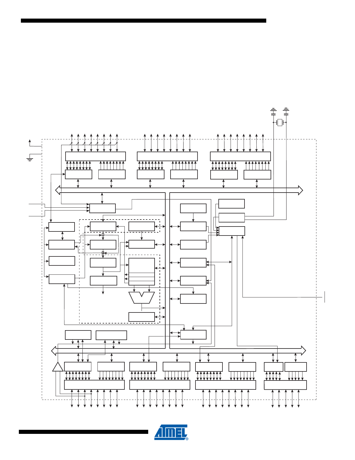
2.1
Block Diagram
Figure 2-1.
Block Diagram
PROGRAM
COUNTER
INTERNAL
OSCILLATOR
WATCHDOG
TIMER
STACK
POINTER
PROGRAM
FLASH
MCU CONTROL
REGISTER
SRAM
GENERAL
PURPOSE
REGISTERS
INSTRUCTION
REGISTER
TIMER/
COUNTERS
INSTRUCTION
DECODER
DATA DIR.
REG. PORTB
DATA DIR.
REG. PORTE
DATA DIR.
REG. PORTA
DATA DIR.
REG. PORTD
DATA REGISTER
PORTB
DATA REGISTER
PORTE
DATA REGISTER
PORTA
DATA REGISTER
PORTD
TIMING AND
CONTROL
OSCILLATOR
INTERRUPT
UNIT
EEPROM
SPI
USART
STATUS
REGISTER
Z
Y
X
ALU
PORTB DRIVERS
PORTE DRIVERS
PORTA DRIVERS
PORTF DRIVERS
PORTD DRIVERS
PORTC DRIVERS
PB0 - PB7
PE0 - PE7
PA0 - PA7
PF0 - PF7
VCC
GND
AREF
XT
AL1
XT
AL2
CONTROL
LINES
+
-
ANALOG
COMP
ARA
T
O
R
PC0 - PC7
8-BIT DATA BUS
RESET
AVCC
CALIB. OSC
DATA DIR.
REG. PORTC
DATA REGISTER
PORTC
ON-CHIP DEBUG
JTAG TAP
PROGRAMMING
LOGIC
BOUNDARY-
SCAN
DATA DIR.
REG. PORTF
DATA REGISTER
PORTF
ADC
PD0 - PD7
DATA DIR.
REG. PORTG
DATA REG.
PORTG
PORTG DRIVERS
PG0 - PG4
UNIVERSAL
SERIAL INTERFACE
AVR CPU

4
8019KS–AVR–11/10
ATmega165P
The AVR core combines a rich instruction set with 32 general purpose working registers. All the
32 registers are directly connected to the Arithmetic Logic Unit (ALU), allowing two independent
registers to be accessed in one single instruction executed in one clock cycle. The resulting
architecture is more code efficient while achieving throughputs up to ten times faster than con-
ventional CISC microcontrollers.
The ATmega165P provides the following features: 16 Kbytes of In-System Programmable Flash
with Read-While-Write capabilities, 512 bytes EEPROM, 1 Kbyte SRAM, 53 general purpose I/O
lines, 32 general purpose working registers, a JTAG interface for Boundary-scan, On-chip
Debugging support and programming, three flexible Timer/Counters with compare modes, inter-
nal and external interrupts, a serial programmable USART, Universal Serial Interface with Start
Condition Detector, an 8-channel, 10-bit ADC, a programmable Watchdog Timer with internal
Oscillator, an SPI serial port, and five software selectable power saving modes. The Idle mode
stops the CPU while allowing the SRAM, Timer/Counters, SPI port, and interrupt system to con-
tinue functioning. The Power-down mode saves the register contents but freezes the Oscillator,
disabling all other chip functions until the next interrupt or hardware reset. In Power-save mode,
the asynchronous timer continues to run, allowing the user to maintain a timer base while the
rest of the device is sleeping. The ADC Noise Reduction mode stops the CPU and all I/O mod-
ules except asynchronous timer and ADC, to minimize switching noise during ADC conversions.
In Standby mode, the crystal/resonator Oscillator is running while the rest of the device is sleep-
ing. This allows very fast start-up combined with low-power consumption.
The device is manufactured using Atmel’s high density non-volatile memory technology. The
On-chip ISP Flash allows the program memory to be reprogrammed In-System through an SPI
serial interface, by a conventional non-volatile memory programmer, or by an On-chip Boot pro-
gram running on the AVR core. The Boot program can use any interface to download the
application program in the Application Flash memory. Software in the Boot Flash section will
continue to run while the Application Flash section is updated, providing true Read-While-Write
operation. By combining an 8-bit RISC CPU with In-System Self-Programmable Flash on a
monolithic chip, the Atmel ATmega165P is a powerful microcontroller that provides a highly flex-
ible and cost effective solution to many embedded control applications.
The ATmega165P AVR is supported with a full suite of program and system development tools
including: C Compilers, Macro Assemblers, Program Debugger/Simulators, In-Circuit Emulators,
and Evaluation kits.

5
8019KS–AVR–11/10
ATmega165P
2.2
Pin Descriptions
2.2.1
VCC
Digital supply voltage.
2.2.2
GND
Ground.
2.2.3
Port A (PA7..PA0)
Port A is an 8-bit bi-directional I/O port with internal pull-up resistors (selected for each bit). The
Port A output buffers have symmetrical drive characteristics with both high sink and source
capability. As inputs, Port A pins that are externally pulled low will source current if the pull-up
resistors are activated. The Port A pins are tri-stated when a reset condition becomes active,
even if the clock is not running.
2.2.4
Port B (PB7:PB0)
Port B is an 8-bit bi-directional I/O port with internal pull-up resistors (selected for each bit). The
Port B output buffers have symmetrical drive characteristics with both high sink and source
capability. As inputs, Port B pins that are externally pulled low will source current if the pull-up
resistors are activated. The Port B pins are tri-stated when a reset condition becomes active,
even if the clock is not running.
Port B has better driving capabilities than the other ports.
Port B also serves the functions of various special features of the ATmega165P as listed on
“Alternate Functions of Port B” on page 69
.
2.2.5
Port C (PC7:PC0)
Port C is an 8-bit bi-directional I/O port with internal pull-up resistors (selected for each bit). The
Port C output buffers have symmetrical drive characteristics with both high sink and source
capability. As inputs, Port C pins that are externally pulled low will source current if the pull-up
resistors are activated. The Port C pins are tri-stated when a reset condition becomes active,
even if the clock is not running.
2.2.6
Port D (PD7:PD0)
Port D is an 8-bit bi-directional I/O port with internal pull-up resistors (selected for each bit). The
Port D output buffers have symmetrical drive characteristics with both high sink and source
capability. As inputs, Port D pins that are externally pulled low will source current if the pull-up
resistors are activated. The Port D pins are tri-stated when a reset condition becomes active,
even if the clock is not running.
Port D also serves the functions of various special features of the ATmega165P as listed on
“Alternate Functions of Port D” on page 72
.
2.2.7
Port E (PE7:PE0)
Port E is an 8-bit bi-directional I/O port with internal pull-up resistors (selected for each bit). The
Port E output buffers have symmetrical drive characteristics with both high sink and source
capability. As inputs, Port E pins that are externally pulled low will source current if the pull-up

6
8019KS–AVR–11/10
ATmega165P
resistors are activated. The Port E pins are tri-stated when a reset condition becomes active,
even if the clock is not running.
Port E also serves the functions of various special features of the ATmega165P as listed in
Chapter
“Alternate Functions of Port E” on page 73
.
2.2.8
Port F (PF7:PF0)
Port F serves as the analog inputs to the A/D Converter.
Port F also serves as an 8-bit bi-directional I/O port, if the A/D Converter is not used. Port pins
can provide internal pull-up resistors (selected for each bit). The Port F output buffers have sym-
metrical drive characteristics with both high sink and source capability. As inputs, Port F pins
that are externally pulled low will source current if the pull-up resistors are activated. The Port F
pins are tri-stated when a reset condition becomes active, even if the clock is not running. If the
JTAG interface is enabled, the pull-up resistors on pins PF7(TDI), PF5(TMS), and PF4(TCK) will
be activated even if a reset occurs.
Port F also serves the functions of the JTAG interface, see
“Alternate Functions of Port F” on
page 75
.
2.2.9
Port G (PG5:PG0)
Port G is a 6-bit bi-directional I/O port with internal pull-up resistors (selected for each bit). The
Port G output buffers have symmetrical drive characteristics with both high sink and source
capability. As inputs, Port G pins that are externally pulled low will source current if the pull-up
resistors are activated. The Port G pins are tri-stated when a reset condition becomes active,
even if the clock is not running.
Port G also serves the functions of various special features of the ATmega165P as listed in
Chapter
“Alternate Functions of Port G” on page 77
.
2.2.10
RESET
Reset input. A low level on this pin for longer than the minimum pulse length will generate a
reset, even if the clock is not running. The minimum pulse length is given in
Table 26-4 on page
302
. Shorter pulses are not guaranteed to generate a reset.
2.2.11
XTAL1
Input to the inverting Oscillator amplifier and input to the internal clock operating circuit.
2.2.12
XTAL2
Output from the inverting Oscillator amplifier.
2.2.13
AVCC
AVCC is the supply voltage pin for Port F and the A/D Converter. It should be externally con-
nected to V
CC
, even if the ADC is not used. If the ADC is used, it should be connected to V
CC
through a low-pass filter.
2.2.14
AREF
This is the analog reference pin for the A/D Converter.

7
8019KS–AVR–11/10
ATmega165P
3.
Resources
A comprehensive set of development tools, application notes and datasheets are available for
download on http://www.atmel.com/avr.
8
8019KS–AVR–11/10
ATmega165P
4.
Register Summary
Address
Name
Bit 7
Bit 6
Bit 5
Bit 4
Bit 3
Bit 2
Bit 1
Bit 0
Page
(0xFF)
Reserved
–
–
–
–
–
–
–
–
(0xFE)
Reserved
–
–
–
–
–
–
–
–
(0xFD)
Reserved
–
–
–
–
–
–
–
–
(0xFC)
Reserved
–
–
–
–
–
–
–
–
(0xFB)
Reserved
–
–
–
–
–
–
–
–
(0xFA)
Reserved
–
–
–
–
–
–
–
–
(0xF9)
Reserved
–
–
–
–
–
–
–
–
(0xF8)
Reserved
–
–
–
–
–
–
–
–
(0xF7)
Reserved
–
–
–
–
–
–
–
–
(0xF6)
Reserved
–
–
–
–
–
–
–
–
(0xF5)
Reserved
–
–
–
–
–
–
–
–
(0xF4)
Reserved
–
–
–
–
–
–
–
–
(0xF3)
Reserved
–
–
–
–
–
–
–
–
(0xF2)
Reserved
–
–
–
–
–
–
–
–
(0xF1)
Reserved
–
–
–
–
–
–
–
–
(0xF0)
Reserved
–
–
–
–
–
–
–
–
(0xEF)
Reserved
–
–
–
–
–
–
–
–
(0xEE)
Reserved
–
–
–
–
–
–
–
–
(0xED)
Reserved
–
–
–
–
–
–
–
–
(0xEC)
Reserved
–
–
–
–
–
–
–
–
(0xEB)
Reserved
–
–
–
–
–
–
–
–
(0xEA)
Reserved
–
–
–
–
–
–
–
–
(0xE9)
Reserved
–
–
–
–
–
–
–
–
(0xE8)
Reserved
–
–
–
–
–
–
–
–
(0xE7)
Reserved
–
–
–
–
–
–
–
–
(0xE6)
Reserved
–
–
–
–
–
–
–
–
(0xE5)
Reserved
–
–
–
–
–
–
–
–
(0xE4)
Reserved
–
–
–
–
–
–
–
–
(0xE3)
Reserved
–
–
–
–
–
–
–
–
(0xE2)
Reserved
–
–
–
–
–
–
–
–
(0xE1)
Reserved
–
–
–
–
–
–
–
–
(0xE0)
Reserved
–
–
–
–
–
–
–
–
(0xDF)
Reserved
–
–
–
–
–
–
–
–
(0xDE)
Reserved
–
–
–
–
–
–
–
–
(0xDD)
Reserved
–
–
–
–
–
–
–
–
(0xDC)
Reserved
–
–
–
–
–
–
–
–
(0xDB)
Reserved
–
–
–
–
–
–
–
–
(0xDA)
Reserved
–
–
–
–
–
–
–
–
(0xD9)
Reserved
–
–
–
–
–
–
–
–
(0xD8)
Reserved
–
–
–
–
–
–
–
–
(0xD7)
Reserved
–
–
–
–
–
–
–
–
(0xD6)
Reserved
–
–
–
–
–
–
–
–
(0xD5)
Reserved
–
–
–
–
–
–
–
–
(0xD4)
Reserved
–
–
–
–
–
–
–
–
(0xD3)
Reserved
–
–
–
–
–
–
–
–
(0xD2)
Reserved
–
–
–
–
–
–
–
–
(0xD1)
Reserved
–
–
–
–
–
–
–
–
(0xD0)
Reserved
–
–
–
–
–
–
–
–
(0xCF)
Reserved
–
–
–
–
–
–
–
–
(0xCE)
Reserved
–
–
–
–
–
–
–
–
(0xCD)
Reserved
–
–
–
–
–
–
–
–
(0xCC)
Reserved
–
–
–
–
–
–
–
–
(0xCB)
Reserved
–
–
–
–
–
–
–
–
(0xCA)
Reserved
–
–
–
–
–
–
–
–
(0xC9)
Reserved
–
–
–
–
–
–
–
–
(0xC8)
Reserved
–
–
–
–
–
–
–
–
(0xC7)
Reserved
–
–
–
–
–
–
–
–
(0xC6)
UDR0
USART0 I/O Data Register
183
(0xC5)
UBRR0H
USART0 Baud Rate Register High
187
(0xC4)
UBRR0L
USART0 Baud Rate Register Low
187
(0xC3)
Reserved
–
–
–
–
–
–
–
–
(0xC2)
UCSR0C
–
UMSEL0
UPM01
UPM00
USBS0
UCSZ01
UCSZ00
UCPOL0
183
(0xC1)
UCSR0B
RXCIE0
TXCIE0
UDRIE0
RXEN0
TXEN0
UCSZ02
RXB80
TXB80
183
(0xC0)
UCSR0A
RXC0
TXC0
UDRE0
FE0
DOR0
UPE0
U2X0
MPCM0
183
9
8019KS–AVR–11/10
ATmega165P
(0xBF)
Reserved
–
–
–
–
–
–
–
–
(0xBE)
Reserved
–
–
–
–
–
–
–
–
(0xBD)
Reserved
–
–
–
–
–
–
–
–
(0xBC)
Reserved
–
–
–
–
–
–
–
–
(0xBB)
Reserved
–
–
–
–
–
–
–
–
(0xBA)
USIDR
USI Data Register
196
(0xB9)
USISR
USISIF
USIOIF
USIPF
USIDC
USICNT3
USICNT2
USICNT1
USICNT0
196
(0xB8)
USICR
USISIE
USIOIE
USIWM1
USIWM0
USICS1
USICS0
USICLK
USITC
197
(0xB7)
Reserved
–
–
–
–
–
–
–
(0xB6)
ASSR
–
–
–
EXCLK
AS2
TCN2UB
OCR2UB
TCR2UB
146
(0xB5)
Reserved
–
–
–
–
–
–
–
–
(0xB4)
Reserved
–
–
–
–
–
–
–
–
(0xB3)
OCR2A
Timer/Counter2 Output Compare Register A
145
(0xB2)
TCNT2
Timer/Counter2 (8-bit)
145
(0xB1)
Reserved
–
–
–
–
–
–
–
–
(0xB0)
TCCR2A
FOC2A
WGM20
COM2A1
COM2A0
WGM21
CS22
CS21
CS20
143
(0xAF)
Reserved
–
–
–
–
–
–
–
–
(0xAE)
Reserved
–
–
–
–
–
–
–
–
(0xAD)
Reserved
–
–
–
–
–
–
–
–
(0xAC)
Reserved
–
–
–
–
–
–
–
–
(0xAB)
Reserved
–
–
–
–
–
–
–
–
(0xAA)
Reserved
–
–
–
–
–
–
–
–
(0xA9)
Reserved
–
–
–
–
–
–
–
–
(0xA8)
Reserved
–
–
–
–
–
–
–
–
(0xA7)
Reserved
–
–
–
–
–
–
–
–
(0xA6)
Reserved
–
–
–
–
–
–
–
–
(0xA5)
Reserved
–
–
–
–
–
–
–
–
(0xA4)
Reserved
–
–
–
–
–
–
–
–
(0xA3)
Reserved
–
–
–
–
–
–
–
–
(0xA2)
Reserved
–
–
–
–
–
–
–
–
(0xA1)
Reserved
–
–
–
–
–
–
–
–
(0xA0)
Reserved
–
–
–
–
–
–
–
–
(0x9F)
Reserved
–
–
–
–
–
–
–
–
(0x9E)
Reserved
–
–
–
–
–
–
–
–
(0x9D)
Reserved
–
–
–
–
–
–
–
–
(0x9C)
Reserved
–
–
–
–
–
–
–
–
(0x9B)
Reserved
–
–
–
–
–
–
–
–
(0x9A)
Reserved
–
–
–
–
–
–
–
–
(0x99)
Reserved
–
–
–
–
–
–
–
–
(0x98)
Reserved
–
–
–
–
–
–
–
–
(0x97)
Reserved
–
–
–
–
–
–
–
–
(0x96)
Reserved
–
–
–
–
–
–
–
–
(0x95)
Reserved
–
–
–
–
–
–
–
–
(0x94)
Reserved
–
–
–
–
–
–
–
–
(0x93)
Reserved
–
–
–
–
–
–
–
–
(0x92)
Reserved
–
–
–
–
–
–
–
–
(0x91)
Reserved
–
–
–
–
–
–
–
–
(0x90)
Reserved
–
–
–
–
–
–
–
–
(0x8F)
Reserved
–
–
–
–
–
–
–
–
(0x8E)
Reserved
–
–
–
–
–
–
–
–
(0x8D)
Reserved
–
–
–
–
–
–
–
–
(0x8C)
Reserved
–
–
–
–
–
–
–
–
(0x8B)
OCR1BH
Timer/Counter1 - Output Compare Register B High Byte
123
(0x8A)
OCR1BL
Timer/Counter1 - Output Compare Register B Low Byte
123
(0x89)
OCR1AH
Timer/Counter1 - Output Compare Register A High Byte
123
(0x88)
OCR1AL
Timer/Counter1 - Output Compare Register A Low Byte
123
(0x87)
ICR1H
Timer/Counter1 - Input Capture Register High Byte
124
(0x86)
ICR1L
Timer/Counter1 - Input Capture Register Low Byte
124
(0x85)
TCNT1H
Timer/Counter1 - Counter Register High Byte
123
(0x84)
TCNT1L
Timer/Counter1 - Counter Register Low Byte
123
(0x83)
Reserved
–
–
–
–
–
–
–
–
(0x82)
TCCR1C
FOC1A
FOC1B
–
–
–
–
–
–
122
(0x81)
TCCR1B
ICNC1
ICES1
–
WGM13
WGM12
CS12
CS11
CS10
121
(0x80)
TCCR1A
COM1A1
COM1A0
COM1B1
COM1B0
–
–
WGM11
WGM10
119
(0x7F)
DIDR1
–
–
–
–
–
–
AIN1D
AIN0D
203
(0x7E)
DIDR0
ADC7D
ADC6D
ADC5D
ADC4D
ADC3D
ADC2D
ADC1D
ADC0D
221
Address
Name
Bit 7
Bit 6
Bit 5
Bit 4
Bit 3
Bit 2
Bit 1
Bit 0
Page
10
8019KS–AVR–11/10
ATmega165P
(0x7D)
Reserved
–
–
–
–
–
–
–
–
(0x7C)
ADMUX
REFS1
REFS0
ADLAR
MUX4
MUX3
MUX2
MUX1
MUX0
217
(0x7B)
ADCSRB
–
ACME
–
–
–
ADTS2
ADTS1
ADTS0
202, 221
(0x7A)
ADCSRA
ADEN
ADSC
ADATE
ADIF
ADIE
ADPS2
ADPS1
ADPS0
219
(0x79)
ADCH
ADC Data Register High byte
220
(0x78)
ADCL
ADC Data Register Low byte
220
(0x77)
Reserved
–
–
–
–
–
–
–
–
(0x76)
Reserved
–
–
–
–
–
–
–
–
(0x75)
Reserved
–
–
–
–
–
–
–
–
(0x74)
Reserved
–
–
–
–
–
–
–
–
(0x73)
Reserved
–
–
–
–
–
–
–
–
(0x72)
Reserved
–
–
–
–
–
–
–
–
(0x71)
Reserved
–
–
–
–
–
–
–
–
(0x70)
TIMSK2
–
–
–
–
–
–
OCIE2A
TOIE2
146
(0x6F)
TIMSK1
–
–
ICIE1
–
–
OCIE1B
OCIE1A
TOIE1
124
(0x6E)
TIMSK0
–
–
–
–
–
–
OCIE0A
TOIE0
96
(0x6D)
Reserved
–
–
–
–
–
–
–
–
(0x6C)
PCMSK1
PCINT15
PCINT14
PCINT13
PCINT12
PCINT11
PCINT10
PCINT9
PCINT8
59
(0x6B)
PCMSK0
PCINT7
PCINT6
PCINT5
PCINT4
PCINT3
PCINT2
PCINT1
PCINT0
60
(0x6A)
Reserved
–
–
–
–
–
–
–
–
(0x69)
EICRA
–
–
–
–
–
–
ISC01
ISC00
58
(0x68)
Reserved
–
–
–
–
–
–
–
–
(0x67)
Reserved
–
–
–
–
–
–
–
–
(0x66)
OSCCAL
Oscillator Calibration Register
34
(0x65)
Reserved
–
–
–
–
–
–
–
–
(0x64)
PRR
–
–
–
–
PRTIM1
PRSPI
PRUSART0
PRADC
41
(0x63)
Reserved
–
–
–
–
–
–
–
–
(0x62)
Reserved
–
–
–
–
–
–
–
–
(0x61)
CLKPR
CLKPCE
–
–
–
CLKPS3
CLKPS2
CLKPS1
CLKPS0
34
(0x60)
WDTCR
–
–
–
WDCE
WDE
WDP2
WDP1
WDP0
50
0x3F (0x5F)
SREG
I
T
H
S
V
N
Z
C
14
0x3E (0x5E)
SPH
–
–
–
–
–
SP10
SP9
SP8
10
0x3D (0x5D)
SPL
SP7
SP6
SP5
SP4
SP3
SP2
SP1
SP0
10
0x3C (0x5C)
Reserved
0x3B (0x5B)
Reserved
0x3A (0x5A)
Reserved
0x39 (0x59)
Reserved
0x38 (0x58)
Reserved
0x37 (0x57)
SPMCSR
SPMIE
RWWSB
–
RWWSRE
BLBSET
PGWRT
PGERS
SPMEN
264
0x36 (0x56)
Reserved
–
–
–
–
–
–
–
–
0x35 (0x55)
MCUCR
JTD
–
–
PUD
–
–
IVSEL
IVCE
56, 79, 249
0x34 (0x54)
MCUSR
–
–
–
JTRF
WDRF
BORF
EXTRF
PORF
249
0x33 (0x53)
SMCR
–
–
–
–
SM2
SM1
SM0
SE
41
0x32 (0x52)
Reserved
–
–
–
–
–
–
–
–
0x31 (0x51)
OCDR
IDRD/OCD
OCDR6
OCDR5
OCDR4
OCDR3
OCDR2
OCDR1
OCDR0
228
0x30 (0x50)
ACSR
ACD
ACBG
ACO
ACI
ACIE
ACIC
ACIS1
ACIS0
202
0x2F (0x4F)
Reserved
–
–
–
–
–
–
–
–
0x2E (0x4E)
SPDR
SPI Data Register
157
0x2D (0x4D)
SPSR
SPIF
WCOL
–
–
–
–
–
SPI2X
156
0x2C (0x4C)
SPCR
SPIE
SPE
DORD
MSTR
CPOL
CPHA
SPR1
SPR0
155
0x2B (0x4B)
GPIOR2
General Purpose I/O Register 2
25
0x2A (0x4A)
GPIOR1
General Purpose I/O Register 1
25
0x29 (0x49)
Reserved
–
–
–
–
–
–
–
–
0x28 (0x48)
Reserved
–
–
–
–
–
–
–
–
0x27 (0x47)
OCR0A
Timer/Counter0 Output Compare Register A
95
0x26 (0x46)
TCNT0
Timer/Counter0 (8 Bit)
95
0x25 (0x45)
Reserved
–
–
–
–
–
–
–
–
0x24 (0x44)
TCCR0A
FOC0A
WGM00
COM0A1
COM0A0
WGM01
CS02
CS01
CS00
93
0x23 (0x43)
GTCCR
TSM
–
–
–
–
–
PSR2
PSR10
128, 147
0x22 (0x42)
EEARH
–
–
–
–
–
–
–
EEAR8
24
0x21 (0x41)
EEARL
EEPROM Address Register Low Byte
24
0x20 (0x40)
EEDR
EEPROM Data Register
24
0x1F (0x3F)
EECR
–
–
–
–
EERIE
EEMWE
EEWE
EERE
24
0x1E (0x3E)
GPIOR0
General Purpose I/O Register 0
25
0x1D (0x3D)
EIMSK
PCIE1
PCIE0
–
–
–
–
–
INT0
58
0x1C (0x3C)
EIFR
PCIF1
PCIF0
–
–
–
–
–
INTF0
59
Address
Name
Bit 7
Bit 6
Bit 5
Bit 4
Bit 3
Bit 2
Bit 1
Bit 0
Page