

Features
•
High-performance, Low-power Atmel
®
AVR
®
8-bit Microcontroller
•
Advanced RISC Architecture
– 133 Powerful Instructions – Most Single Clock Cycle Execution
– 32 x 8 General Purpose Working Registers + Peripheral Control Registers
– Fully Static Operation
– Up to 16MIPS Throughput at 16MHz
– On-chip 2-cycle Multiplier
•
High Endurance Non-volatile Memory segments
– 128Kbytes of In-System Self-programmable Flash program memory
– 4Kbytes EEPROM
– 4Kbytes Internal SRAM
– Write/Erase cycles: 10,000 Flash/100,000 EEPROM
– Data retention: 20 years at 85
°C/100 years at 25°C
(1)
– Optional Boot Code Section with Independent Lock Bits
In-System Programming by On-chip Boot Program
True Read-While-Write Operation
– Up to 64Kbytes Optional External Memory Space
– Programming Lock for Software Security
– SPI Interface for In-System Programming
•
QTouch
®
library support
– Capacitive touch buttons, sliders and wheels
– QTouch and QMatrix acquisition
– Up to 64 sense channels
•
JTAG (IEEE std. 1149.1 Compliant) Interface
– Boundary-scan Capabilities According to the JTAG Standard
– Extensive On-chip Debug Support
– Programming of Flash, EEPROM, Fuses and Lock Bits through the JTAG Interface
•
Peripheral Features
– Two 8-bit Timer/Counters with Separate Prescalers and Compare Modes
– Two Expanded 16-bit Timer/Counters with Separate Prescaler, Compare Mode and Capture
Mode
– Real Time Counter with Separate Oscillator
– Two 8-bit PWM Channels
– 6 PWM Channels with Programmable Resolution from 2 to 16 Bits
– Output Compare Modulator
– 8-channel, 10-bit ADC
8 Single-ended Channels
7 Differential Channels
2 Differential Channels with Programmable Gain at 1x, 10x, or 200x
– Byte-oriented Two-wire Serial Interface
– Dual Programmable Serial USARTs
– Master/Slave SPI Serial Interface
– Programmable Watchdog Timer with On-chip Oscillator
– On-chip Analog Comparator
•
Special Microcontroller Features
– Power-on Reset and Programmable Brown-out Detection
– Internal Calibrated RC Oscillator
– External and Internal Interrupt Sources
– Six Sleep Modes: Idle, ADC Noise Reduction, Power-save, Power-down, Standby, and
Extended Standby
– Software Selectable Clock Frequency
– ATmega103 Compatibility Mode Selected by a Fuse
– Global Pull-up Disable
•
I/O and Packages
– 53 Programmable I/O Lines
– 64-lead TQFP and 64-pad QFN/MLF
•
Operating Voltages
– 2.7 - 5.5V ATmega128L
– 4.5 - 5.5V ATmega128
•
Speed Grades
– 0 - 8MHz ATmega128L
– 0 - 16MHz ATmega128
8-bit Atmel
Microcontroller
with 128KBytes
In-System
Programmable
Flash
ATmega128
ATmega128L
Summary
Rev. 2467XS–AVR–06/11
2
2467XS–AVR–06/11
ATmega128
Pin
Configurations
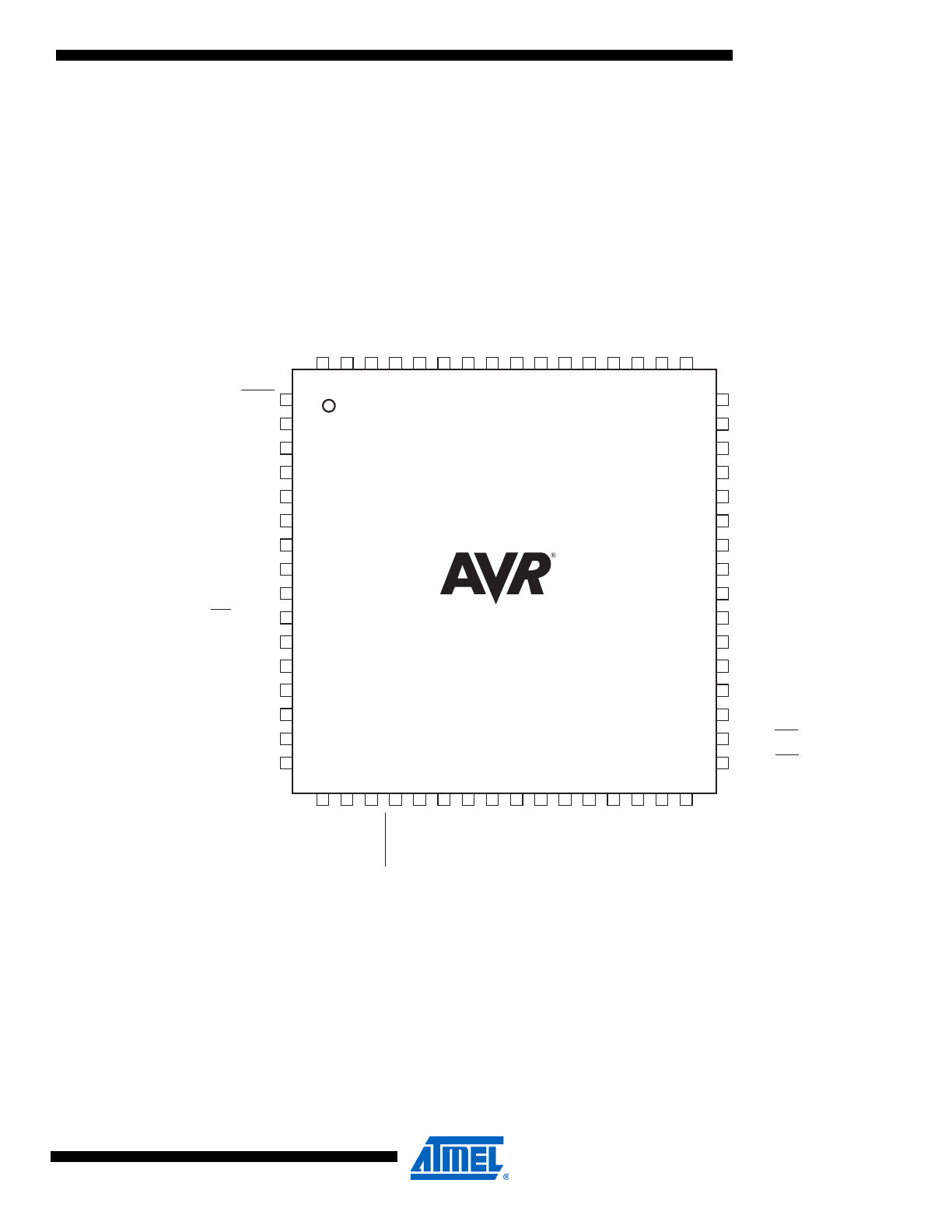
Figure 1. Pinout ATmega128
Note:
The Pinout figure applies to both TQFP and MLF packages. The bottom pad under the QFN/MLF
package should be soldered to ground.
Overview
The Atmel
®
AVR
®
ATmega128 is a low-power CMOS 8-bit microcontroller based on the AVR
enhanced RISC architecture. By executing powerful instructions in a single clock cycle, the
ATmega128 achieves throughputs approaching 1MIPS per MHz allowing the system designer to
optimize power consumption versus processing speed.
1
2
3
4
5
6
7
8
9
10
11
12
13
14
15
16
48
47
46
45
44
43
42
41
40
39
38
37
36
35
34
33
PEN
RXD0/(PDI) PE0
(TXD0/PDO) PE1
(XCK0/AIN0) PE2
(OC3A/AIN1) PE3
(OC3B/INT4) PE4
(OC3C/INT5) PE5
(T3/INT6) PE6
(ICP3/INT7) PE7
(SS) PB0
(SCK) PB1
(MOSI) PB2
(MISO) PB3
(OC0) PB4
(OC1A) PB5
(OC1B) PB6
PA3 (AD3)
PA4 (AD4)
PA5 (AD5)
PA6 (AD6)
PA7 (AD7)
PG2(ALE)
PC7 (A15)
PC6 (A14)
PC5 (A13)
PC4 (A12)
PC3 (A11)
PC2 (A10)
PC1 (A9)
PC0 (A8)
PG1(RD)
PG0(WR)
64
63
62
61
60
59
5
8
57
56
55
54
53
52
51
50
49
17
1
8
19
20
21
22
23
24
25
26
27
2
8
29
30
31
32
(OC2/OC1C) PB7
TOSC2/PG3
TOSC1/PG4
RESET
V
CC
G
N
D
XTAL2
XTAL1
(SCL/I
N
T0) PD0
(SDA/I
N
T1) PD1
(RXD1/I
N
T2) PD2
(TXD1/I
N
T3) PD3
(ICP1) PD4
(XCK1) PD5
(T1) PD6
(T2) PD7
A
V
CC
G
N
D
AREF
PF0 (ADC0)
PF1 (ADC1)
PF2 (ADC2)
PF3 (ADC3)
PF4 (ADC4/TCK)
PF5 (ADC5/TMS)
PF6 (ADC6/TDO)
PF7 (ADC7/TDI)
G
N
D
V
CC
PA0 (AD0)
PA1 (AD1)
PA2 (AD2)
3
2467XS–AVR–06/11
ATmega128
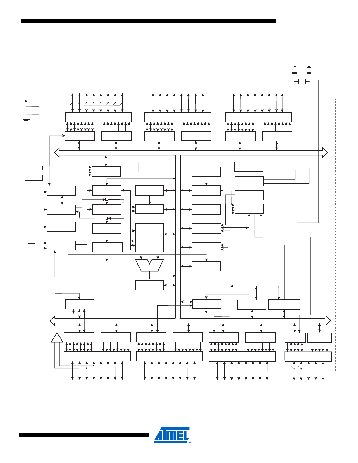
Block Diagram
Figure 2. Block Diagram
PROGRAM
COUNTER
INTERNAL
OSCILLATOR
WATCHDOG
TIMER
STACK
POINTER
PROGRAM
FLASH
MCU CONTROL
REGISTER
SRAM
GENERAL
PURPOSE
REGISTERS
INSTRUCTION
REGISTER
TIMER/
COUNTERS
INSTRUCTION
DECODER
DATA DIR.
REG. PORTB
DATA DIR.
REG. PORTE
DATA DIR.
REG. PORTA
DATA DIR.
REG. PORTD
DATA REGISTER
PORTB
DATA REGISTER
PORTE
DATA REGISTER
PORTA
DATA REGISTER
PORTD
TIMING AND
CONTROL
OSCILLATOR
OSCILLATOR
INTERRUPT
UNIT
EEPROM
SPI
USART0
STATUS
REGISTER
Z
Y
X
ALU
PORTB DRIVERS
PORTE DRIVERS
PORTA DRIVERS
PORTF DRIVERS
PORTD DRIVERS
PORTC DRIVERS
PB0 - PB7
PE0 - PE7
PA0 - PA7
PF0 - PF7
RESET
VCC
AGND
GND
AREF
XT
AL1
XT
AL2
CONTROL
LINES
+
-
ANALOG
COMP
ARA
T
O
R
PC0 - PC7
8-BIT DATA BUS
AVCC
USART1
CALIB. OSC
DATA DIR.
REG. PORTC
DATA REGISTER
PORTC
ON-CHIP DEBUG
JTAG TAP
PROGRAMMING
LOGIC
PEN
BOUNDARY-
SCAN
DATA DIR.
REG. PORTF
DATA REGISTER
PORTF
ADC
PD0 - PD7
DATA DIR.
REG. PORTG
DATA REG.
PORTG
PORTG DRIVERS
PG0 - PG4
TWO-WIRE SERIAL
INTERFACE

4
2467XS–AVR–06/11
ATmega128
The Atmel
®
AVR
®
core combines a rich instruction set with 32 general purpose working regis-
ters. All the 32 registers are directly connected to the Arithmetic Logic Unit (ALU), allowing two
independent registers to be accessed in one single instruction executed in one clock cycle. The
resulting architecture is more code efficient while achieving throughputs up to ten times faster
than conventional CISC microcontrollers.
The ATmega128 provides the following features: 128Kbytes of In-System Programmable Flash
with Read-While-Write capabilities, 4Kbytes EEPROM, 4Kbytes SRAM, 53 general purpose I/O
lines, 32 general purpose working registers, Real Time Counter (RTC), four flexible Timer/Coun-
ters with compare modes and PWM, 2 USARTs, a byte oriented Two-wire Serial Interface, an 8-
channel, 10-bit ADC with optional differential input stage with programmable gain, programma-
ble Watchdog Timer with Internal Oscillator, an SPI serial port, IEEE std. 1149.1 compliant
JTAG test interface, also used for accessing the On-chip Debug system and programming and
six software selectable power saving modes. The Idle mode stops the CPU while allowing the
SRAM, Timer/Counters, SPI port, and interrupt system to continue functioning. The Power-down
mode saves the register contents but freezes the Oscillator, disabling all other chip functions
until the next interrupt or Hardware Reset. In Power-save mode, the asynchronous timer contin-
ues to run, allowing the user to maintain a timer base while the rest of the device is sleeping.
The ADC Noise Reduction mode stops the CPU and all I/O modules except Asynchronous
Timer and ADC, to minimize switching noise during ADC conversions. In Standby mode, the
Crystal/Resonator Oscillator is running while the rest of the device is sleeping. This allows very
fast start-up combined with low power consumption. In Extended Standby mode, both the main
Oscillator and the Asynchronous Timer continue to run.
Atmel offers the QTouch
®
library for embedding capacitive touch buttons, sliders and wheels
functionality into AVR microcontrollers. The patented charge-transfer signal acquisition offers
robust sensing and includes fully debounced reporting of touch keys and includes Adjacent Key
Suppression
®
(AKS
™
) technology for unambiguous detection of key events. The easy-to-use
QTouch Suite toolchain allows you to explore, develop and debug your own touch applications.
The device is manufactured using Atmel’s high-density nonvolatile memory technology. The On-
chip ISP Flash allows the program memory to be reprogrammed in-system through an SPI serial
interface, by a conventional nonvolatile memory programmer, or by an On-chip Boot program
running on the AVR core. The boot program can use any interface to download the application
program in the application Flash memory. Software in the Boot Flash section will continue to run
while the Application Flash section is updated, providing true Read-While-Write operation. By
combining an 8-bit RISC CPU with In-System Self-Programmable Flash on a monolithic chip,
the Atmel ATmega128 is a powerful microcontroller that provides a highly flexible and cost effec-
tive solution to many embedded control applications.
The ATmega128 device is supported with a full suite of program and system development tools
including: C compilers, macro assemblers, program debugger/simulators, in-circuit emulators,
and evaluation kits.
ATmega103 and
ATmega128
Compatibility
The ATmega128 is a highly complex microcontroller where the number of I/O locations super-
sedes the 64 I/O locations reserved in the AVR instruction set. To ensure backward compatibility
with the ATmega103, all I/O locations present in ATmega103 have the same location in
ATmega128. Most additional I/O locations are added in an Extended I/O space starting from $60
to $FF, (i.e., in the ATmega103 internal RAM space). These locations can be reached by using
LD/LDS/LDD and ST/STS/STD instructions only, not by using IN and OUT instructions. The relo-
cation of the internal RAM space may still be a problem for ATmega103 users. Also, the
increased number of interrupt vectors might be a problem if the code uses absolute addresses.
To solve these problems, an ATmega103 compatibility mode can be selected by programming
the fuse M103C. In this mode, none of the functions in the Extended I/O space are in use, so the
internal RAM is located as in ATmega103. Also, the Extended Interrupt vectors are removed.

5
2467XS–AVR–06/11
ATmega128
The ATmega128 is 100% pin compatible with ATmega103, and can replace the ATmega103 on
current Printed Circuit Boards. The application note “Replacing ATmega103 by ATmega128”
describes what the user should be aware of replacing the ATmega103 by an ATmega128.
ATmega103
Compatibility Mode
By programming the M103C fuse, the Atmel
®
ATmega128 will be compatible with the
ATmega103 regards to RAM, I/O pins and interrupt vectors as described above. However, some
new features in ATmega128 are not available in this compatibility mode, these features are
listed below:
•
One USART instead of two, Asynchronous mode only. Only the eight least significant bits of
the Baud Rate Register is available.
•
One 16 bits Timer/Counter with two compare registers instead of two 16-bit Timer/Counters
with three compare registers.
•
Two-wire serial interface is not supported.
•
Port C is output only.
•
Port G serves alternate functions only (not a general I/O port).
•
Port F serves as digital input only in addition to analog input to the ADC.
•
Boot Loader capabilities is not supported.
•
It is not possible to adjust the frequency of the internal calibrated RC Oscillator.
•
The External Memory Interface can not release any Address pins for general I/O, neither
configure different wait-states to different External Memory Address sections.
In addition, there are some other minor differences to make it more compatible to ATmega103:
•
Only EXTRF and PORF exists in MCUCSR.
•
Timed sequence not required for Watchdog Time-out change.
•
External Interrupt pins 3 - 0 serve as level interrupt only.
•
USART has no FIFO buffer, so data overrun comes earlier.
Unused I/O bits in ATmega103 should be written to 0 to ensure same operation in ATmega128.
Pin Descriptions
VCC
Digital supply voltage.
GND
Ground.
Port A (PA7..PA0)
Port A is an 8-bit bi-directional I/O port with internal pull-up resistors (selected for each bit). The
Port A output buffers have symmetrical drive characteristics with both high sink and source
capability. As inputs, Port A pins that are externally pulled low will source current if the pull-up
resistors are activated. The Port A pins are tri-stated when a reset condition becomes active,
even if the clock is not running.
Port A also serves the functions of various special features of the ATmega128 as listed on
page
72
.
Port B (PB7..PB0)
Port B is an 8-bit bi-directional I/O port with internal pull-up resistors (selected for each bit). The
Port B output buffers have symmetrical drive characteristics with both high sink and source
capability. As inputs, Port B pins that are externally pulled low will source current if the pull-up
resistors are activated. The Port B pins are tri-stated when a reset condition becomes active,
even if the clock is not running.
Port B also serves the functions of various special features of the ATmega128 as listed on
page
73
.

6
2467XS–AVR–06/11
ATmega128
Port C (PC7..PC0)
Port C is an 8-bit bi-directional I/O port with internal pull-up resistors (selected for each bit). The
Port C output buffers have symmetrical drive characteristics with both high sink and source
capability. As inputs, Port C pins that are externally pulled low will source current if the pull-up
resistors are activated. The Port C pins are tri-stated when a reset condition becomes active,
even if the clock is not running.
Port C also serves the functions of special features of the Atmel
®
AVR
®
ATmega128 as listed on
page 76
. In ATmega103 compatibility mode, Port C is output only, and the port C pins are not tri-
stated when a reset condition becomes active.
Note:
The ATmega128 is by default shipped in ATmega103 compatibility mode. Thus, if the parts are not
programmed before they are put on the PCB, PORTC will be output during first power up, and until
the ATmega103 compatibility mode is disabled.
Port D (PD7..PD0)
Port D is an 8-bit bi-directional I/O port with internal pull-up resistors (selected for each bit). The
Port D output buffers have symmetrical drive characteristics with both high sink and source
capability. As inputs, Port D pins that are externally pulled low will source current if the pull-up
resistors are activated. The Port D pins are tri-stated when a reset condition becomes active,
even if the clock is not running.
Port D also serves the functions of various special features of the ATmega128 as listed on
page
77
.
Port E (PE7..PE0)
Port E is an 8-bit bi-directional I/O port with internal pull-up resistors (selected for each bit). The
Port E output buffers have symmetrical drive characteristics with both high sink and source
capability. As inputs, Port E pins that are externally pulled low will source current if the pull-up
resistors are activated. The Port E pins are tri-stated when a reset condition becomes active,
even if the clock is not running.
Port E also serves the functions of various special features of the ATmega128 as listed on
page
80
.
Port F (PF7..PF0)
Port F serves as the analog inputs to the A/D Converter.
Port F also serves as an 8-bit bi-directional I/O port, if the A/D Converter is not used. Port pins
can provide internal pull-up resistors (selected for each bit). The Port F output buffers have sym-
metrical drive characteristics with both high sink and source capability. As inputs, Port F pins
that are externally pulled low will source current if the pull-up resistors are activated. The Port F
pins are tri-stated when a reset condition becomes active, even if the clock is not running. If the
JTAG interface is enabled, the pull-up resistors on pins PF7(TDI), PF5(TMS), and PF4(TCK) will
be activated even if a Reset occurs.
The TDO pin is tri-stated unless TAP states that shift out data are entered.
Port F also serves the functions of the JTAG interface.
In ATmega103 compatibility mode, Port F is an input Port only.
Port G (PG4..PG0)
Port G is a 5-bit bi-directional I/O port with internal pull-up resistors (selected for each bit). The
Port G output buffers have symmetrical drive characteristics with both high sink and source
capability. As inputs, Port G pins that are externally pulled low will source current if the pull-up
resistors are activated. The Port G pins are tri-stated when a reset condition becomes active,
even if the clock is not running.
Port G also serves the functions of various special features.
The port G pins are tri-stated when a reset condition becomes active, even if the clock is not
running.

7
2467XS–AVR–06/11
ATmega128
In ATmega103 compatibility mode, these pins only serves as strobes signals to the external
memory as well as input to the 32kHz Oscillator, and the pins are initialized to PG0 = 1, PG1 = 1,
and PG2 = 0 asynchronously when a reset condition becomes active, even if the clock is not
running. PG3 and PG4 are oscillator pins.
RESET
Reset input. A low level on this pin for longer than the minimum pulse length will generate a
reset, even if the clock is not running. The minimum pulse length is given in
Table 19 on page
50
. Shorter pulses are not guaranteed to generate a reset.
XTAL1
Input to the inverting Oscillator amplifier and input to the internal clock operating circuit.
XTAL2
Output from the inverting Oscillator amplifier.
AVCC
AVCC is the supply voltage pin for Port F and the A/D Converter. It should be externally con-
nected to V
CC
, even if the ADC is not used. If the ADC is used, it should be connected to V
CC
through a low-pass filter.
AREF
AREF is the analog reference pin for the A/D Converter.
PEN
PEN is a programming enable pin for the SPI Serial Programming mode, and is internally pulled
high . By holding this pin low during a Power-on Reset, the device will enter the SPI Serial Pro-
gramming mode. PEN has no function during normal operation.

8
2467XS–AVR–06/11
ATmega128
Resources
A comprehensive set of development tools, application notes, and datasheets are available for
download on http://www.atmel.com/avr.
Note:
1.
Data Retention
Reliability Qualification results show that the projected data retention failure rate is much less
than 1 PPM over 20 years at 85°C or 100 years at 25°C
About Code
Examples
This datasheet contains simple code examples that briefly show how to use various parts of the
device. These code examples assume that the part specific header file is included before compi-
lation. Be aware that not all C compiler vendors include bit definitions in the header files and
interrupt handling in C is compiler dependent. Please confirm with the C compiler documentation
for more details.
For I/O registers located in extended I/O map, “IN”, “OUT”, “SBIS”, “SBIC”, “CBI”, and “SBI”
instructions must be replaced with instructions that allow access to extended I/O. Typically
“LDS” and “STS” combined with “SBRS”, “SBRC”, “SBR”, and “CBR”.
Capacitive touch sensing
The Atmel QTouch Library provides a simple to use solution to realize touch sensitive interfaces
on most Atmel AVR microcontrollers. The QTouch Library includes support for the QTouch and
QMatrix acquisition methods.
Touch sensing can be added to any application by linking the appropriate Atmel QTouch Library
for the AVR Microcontroller. This is done by using a simple set of APIs to define the touch chan-
nels and sensors, and then calling the touch sensing API’s to retrieve the channel information
and determine the touch sensor states.
The QTouch Library is FREE and downloadable from the Atmel website at the following location:
www.atmel.com/qtouchlibrary
. For implementation details and other information, refer to the
Atmel QTouch Library User Guide
- also available for download from the Atmel website.
9
2467XS–AVR–06/11
ATmega128
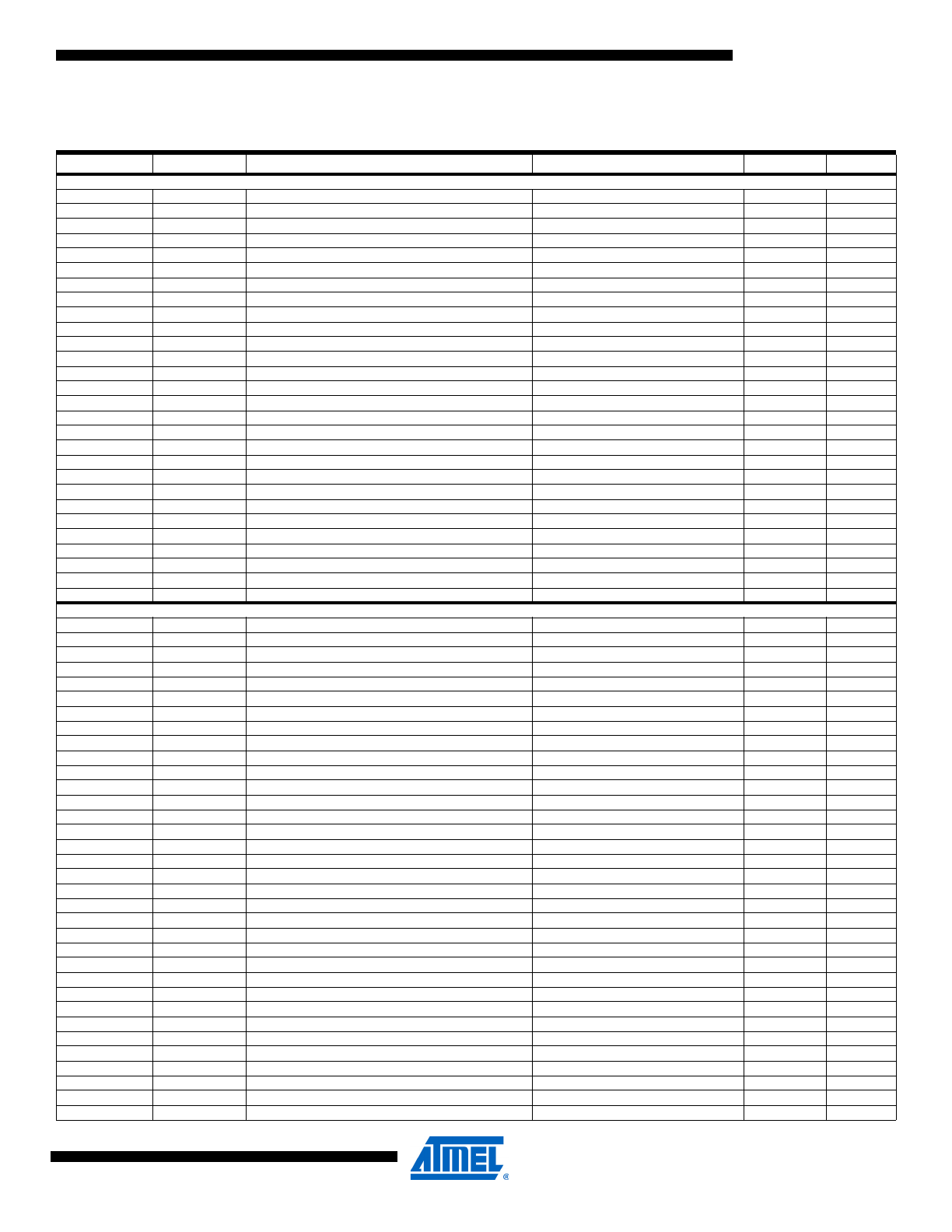
Instruction Set Summary
Mnemonics
Operands
Description
Operation
Flags
#Clocks
ARITHMETIC AND LOGIC INSTRUCTIONS
ADD
Rd, Rr
Add two Registers
Rd
← Rd + Rr
Z,C,N,V,H
1
ADC
Rd, Rr
Add with Carry two Registers
Rd
← Rd + Rr + C
Z,C,N,V,H
1
ADIW
Rdl,K
Add Immediate to Word
Rdh:Rdl
← Rdh:Rdl + K
Z,C,N,V,S
2
SUB
Rd, Rr
Subtract two Registers
Rd
← Rd - Rr
Z,C,N,V,H
1
SUBI
Rd, K
Subtract Constant from Register
Rd
← Rd - K
Z,C,N,V,H
1
SBC
Rd, Rr
Subtract with Carry two Registers
Rd
← Rd - Rr - C
Z,C,N,V,H
1
SBCI
Rd, K
Subtract with Carry Constant from Reg.
Rd
← Rd - K - C
Z,C,N,V,H
1
SBIW
Rdl,K
Subtract Immediate from Word
Rdh:Rdl
← Rdh:Rdl - K
Z,C,N,V,S
2
AND
Rd, Rr
Logical AND Registers
Rd
← Rd • Rr
Z,N,V
1
ANDI
Rd, K
Logical AND Register and Constant
Rd
← Rd • K
Z,N,V
1
OR
Rd, Rr
Logical OR Registers
Rd
← Rd v Rr
Z,N,V
1
ORI
Rd, K
Logical OR Register and Constant
Rd
← Rd v K
Z,N,V
1
EOR
Rd, Rr
Exclusive OR Registers
Rd
← Rd ⊕ Rr
Z,N,V
1
COM
Rd
One’s Complement
Rd
← $FF − Rd
Z,C,N,V
1
NEG
Rd
Two’s Complement
Rd
← $00 − Rd
Z,C,N,V,H
1
SBR
Rd,K
Set Bit(s) in Register
Rd
← Rd v K
Z,N,V
1
CBR
Rd,K
Clear Bit(s) in Register
Rd
← Rd • ($FF - K)
Z,N,V
1
INC
Rd
Increment
Rd
← Rd + 1
Z,N,V
1
DEC
Rd
Decrement
Rd
← Rd − 1
Z,N,V
1
TST
Rd
Test for Zero or Minus
Rd
← Rd • Rd
Z,N,V
1
CLR
Rd
Clear Register
Rd
← Rd ⊕ Rd
Z,N,V
1
SER
Rd
Set Register
Rd
← $FF
None
1
MUL
Rd, Rr
Multiply Unsigned
R1:R0
← Rd x Rr
Z,C
2
MULS
Rd, Rr
Multiply Signed
R1:R0
← Rd x Rr
Z,C
2
MULSU
Rd, Rr
Multiply Signed with Unsigned
R1:R0
← Rd x Rr
Z,C
2
FMUL
Rd, Rr
Fractional Multiply Unsigned
R1:R0
← (Rd x Rr)
<< 1
Z,C
2
FMULS
Rd, Rr
Fractional Multiply Signed
R1:R0
← (Rd x Rr)
<< 1
Z,C
2
FMULSU
Rd, Rr
Fractional Multiply Signed with Unsigned
R1:R0
← (Rd x Rr)
<< 1
Z,C
2
BRANCH INSTRUCTIONS
RJMP
k
Relative Jump
PC
← PC + k + 1
None
2
IJMP
Indirect Jump to (Z)
PC
← Z
None
2
JMP
k
Direct Jump
PC
← k
None
3
RCALL
k
Relative Subroutine Call
PC
← PC + k + 1
None
3
ICALL
Indirect Call to (Z)
PC
← Z
None
3
CALL
k
Direct Subroutine Call
PC
← k
None
4
RET
Subroutine Return
PC
← STACK
None
4
RETI
Interrupt Return
PC
← STACK
I
4
CPSE
Rd,Rr
Compare, Skip if Equal
if (Rd = Rr) PC
← PC + 2 or 3
None
1 / 2 / 3
CP
Rd,Rr
Compare
Rd
− Rr
Z, N,V,C,H
1
CPC
Rd,Rr
Compare with Carry
Rd
− Rr − C
Z, N,V,C,H
1
CPI
Rd,K
Compare Register with Immediate
Rd
− K
Z, N,V,C,H
1
SBRC
Rr, b
Skip if Bit in Register Cleared
if (Rr(b)=0) PC
← PC + 2 or 3
None
1 / 2 / 3
SBRS
Rr, b
Skip if Bit in Register is Set
if (Rr(b)=1) PC
← PC + 2 or 3
None
1 / 2 / 3
SBIC
P, b
Skip if Bit in I/O Register Cleared
if (P(b)=0) PC
← PC + 2 or 3
None
1 / 2 / 3
SBIS
P, b
Skip if Bit in I/O Register is Set
if (P(b)=1) PC
← PC + 2 or 3
None
1 / 2 / 3
BRBS
s, k
Branch if Status Flag Set
if (SREG(s) = 1) then PC
←PC+k + 1
None
1 / 2
BRBC
s, k
Branch if Status Flag Cleared
if (SREG(s) = 0) then PC
←PC+k + 1
None
1 / 2
BREQ
k
Branch if Equal
if (Z = 1) then PC
← PC + k + 1
None
1 / 2
BRNE
k
Branch if Not Equal
if (Z = 0) then PC
← PC + k + 1
None
1 / 2
BRCS
k
Branch if Carry Set
if (C = 1) then PC
← PC + k + 1
None
1 / 2
BRCC
k
Branch if Carry Cleared
if (C = 0) then PC
← PC + k + 1
None
1 / 2
BRSH
k
Branch if Same or Higher
if (C = 0) then PC
← PC + k + 1
None
1 / 2
BRLO
k
Branch if Lower
if (C = 1) then PC
← PC + k + 1
None
1 / 2
BRMI
k
Branch if Minus
if (N = 1) then PC
← PC + k + 1
None
1 / 2
BRPL
k
Branch if Plus
if (N = 0) then PC
← PC + k + 1
None
1 / 2
BRGE
k
Branch if Greater or Equal, Signed
if (N
⊕ V= 0) then PC ← PC + k + 1
None
1 / 2
BRLT
k
Branch if Less Than Zero, Signed
if (N
⊕ V= 1) then PC ← PC + k + 1
None
1 / 2
BRHS
k
Branch if Half Carry Flag Set
if (H = 1) then PC
← PC + k + 1
None
1 / 2
BRHC
k
Branch if Half Carry Flag Cleared
if (H = 0) then PC
← PC + k + 1
None
1 / 2
BRTS
k
Branch if T Flag Set
if (T = 1) then PC
← PC + k + 1
None
1 / 2
BRTC
k
Branch if T Flag Cleared
if (T = 0) then PC
← PC + k + 1
None
1 / 2
BRVS
k
Branch if Overflow Flag is Set
if (V = 1) then PC
← PC + k + 1
None
1 / 2
BRVC
k
Branch if Overflow Flag is Cleared
if (V = 0) then PC
← PC + k + 1
None
1 / 2
10
2467XS–AVR–06/11
ATmega128
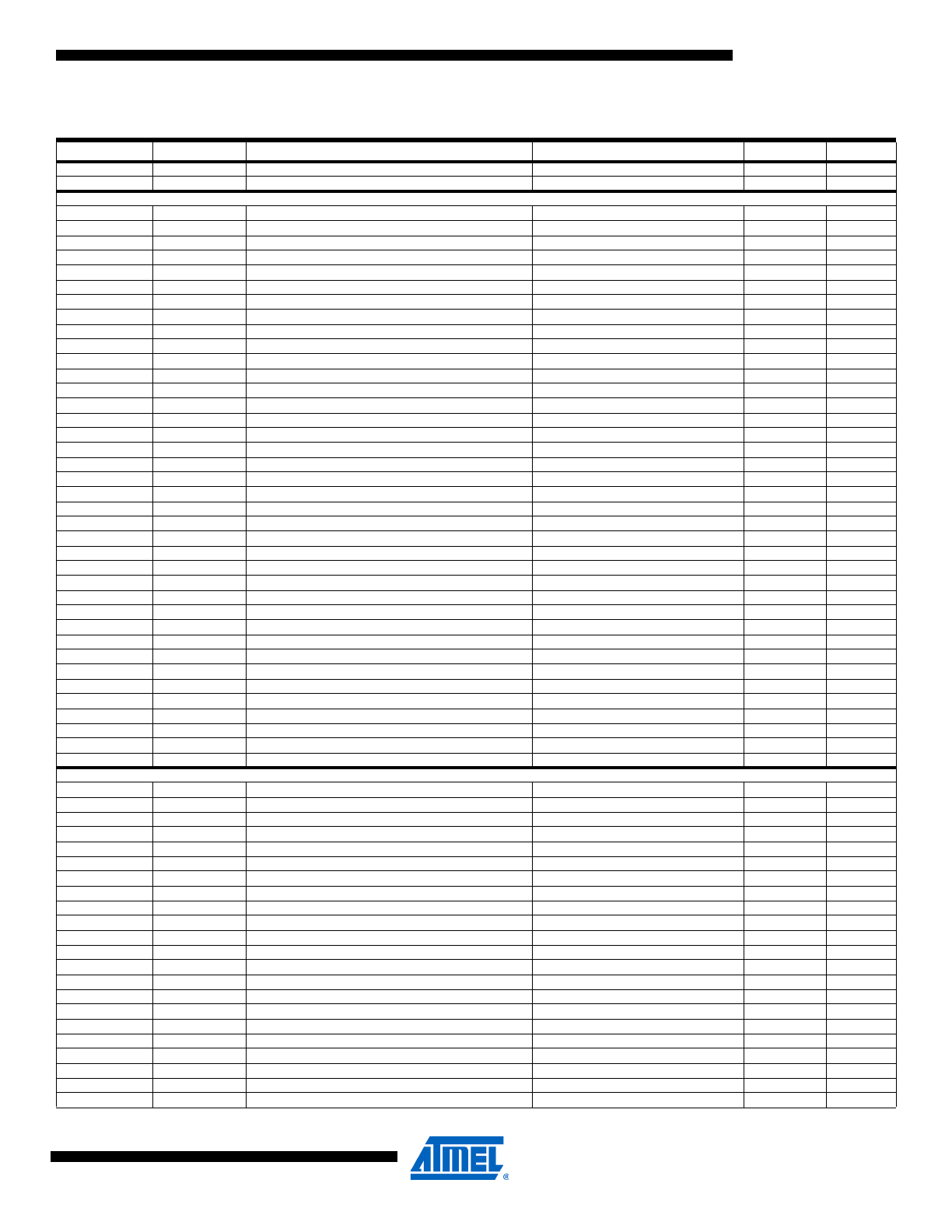
Mnemonics
Operands
Description
Operation
Flags
#Clocks
BRIE
k
Branch if Interrupt Enabled
if ( I = 1) then PC
← PC + k + 1
None
1 / 2
BRID
k
Branch if Interrupt Disabled
if ( I = 0) then PC
← PC + k + 1
None
1 / 2
DATA TRANSFER INSTRUCTIONS
MOV
Rd, Rr
Move Between Registers
Rd
← Rr
None
1
MOVW
Rd, Rr
Copy Register Word
Rd+1:Rd
← Rr+1:Rr
None
1
LDI
Rd, K
Load Immediate
Rd
← K
None
1
LD
Rd, X
Load Indirect
Rd
← (X)
None
2
LD
Rd, X+
Load Indirect and Post-Inc.
Rd
← (X), X ← X + 1
None
2
LD
Rd, - X
Load Indirect and Pre-Dec.
X
← X - 1, Rd ← (X)
None
2
LD
Rd, Y
Load Indirect
Rd
← (Y)
None
2
LD
Rd, Y+
Load Indirect and Post-Inc.
Rd
← (Y), Y ← Y + 1
None
2
LD
Rd, - Y
Load Indirect and Pre-Dec.
Y
← Y - 1, Rd ← (Y)
None
2
LDD
Rd,Y+q
Load Indirect with Displacement
Rd
← (Y + q)
None
2
LD
Rd, Z
Load Indirect
Rd
← (Z)
None
2
LD
Rd, Z+
Load Indirect and Post-Inc.
Rd
← (Z), Z ← Z+1
None
2
LD
Rd, -Z
Load Indirect and Pre-Dec.
Z
← Z - 1, Rd ← (Z)
None
2
LDD
Rd, Z+q
Load Indirect with Displacement
Rd
← (Z + q)
None
2
LDS
Rd, k
Load Direct from SRAM
Rd
← (k)
None
2
ST
X, Rr
Store Indirect
(X)
← Rr
None
2
ST
X+, Rr
Store Indirect and Post-Inc.
(X)
← Rr, X ← X + 1
None
2
ST
- X, Rr
Store Indirect and Pre-Dec.
X
← X - 1, (X) ← Rr
None
2
ST
Y, Rr
Store Indirect
(Y)
← Rr
None
2
ST
Y+, Rr
Store Indirect and Post-Inc.
(Y)
← Rr, Y ← Y + 1
None
2
ST
- Y, Rr
Store Indirect and Pre-Dec.
Y
← Y - 1, (Y) ← Rr
None
2
STD
Y+q,Rr
Store Indirect with Displacement
(Y + q)
← Rr
None
2
ST
Z, Rr
Store Indirect
(Z)
← Rr
None
2
ST
Z+, Rr
Store Indirect and Post-Inc.
(Z)
← Rr, Z ← Z + 1
None
2
ST
-Z, Rr
Store Indirect and Pre-Dec.
Z
← Z - 1, (Z) ← Rr
None
2
STD
Z+q,Rr
Store Indirect with Displacement
(Z + q)
← Rr
None
2
STS
k, Rr
Store Direct to SRAM
(k)
← Rr
None
2
LPM
Load Program Memory
R0
← (Z)
None
3
LPM
Rd, Z
Load Program Memory
Rd
← (Z)
None
3
LPM
Rd, Z+
Load Program Memory and Post-Inc
Rd
← (Z), Z ← Z+1
None
3
ELPM
Extended Load Program Memory
R0
← (RAMPZ:Z)
None
3
ELPM
Rd, Z
Extended Load Program Memory
Rd
← (RAMPZ:Z)
None
3
ELPM
Rd, Z+
Extended Load Program Memory and Post-Inc
Rd
← (RAMPZ:Z), RAMPZ:Z ← RAMPZ:Z+1
None
3
SPM
Store Program Memory
(Z)
← R1:R0
None
-
IN
Rd, P
In Port
Rd
← P
None
1
OUT
P, Rr
Out Port
P
← Rr
None
1
PUSH
Rr
Push Register on Stack
STACK
← Rr
None
2
POP
Rd
Pop Register from Stack
Rd
← STACK
None
2
BIT AND BIT-TEST INSTRUCTIONS
SBI
P,b
Set Bit in I/O Register
I/O(P,b)
← 1
None
2
CBI
P,b
Clear Bit in I/O Register
I/O(P,b)
← 0
None
2
LSL
Rd
Logical Shift Left
Rd(n+1)
← Rd(n), Rd(0) ← 0
Z,C,N,V
1
LSR
Rd
Logical Shift Right
Rd(n)
← Rd(n+1), Rd(7) ← 0
Z,C,N,V
1
ROL
Rd
Rotate Left Through Carry
Rd(0)
←C,Rd(n+1)← Rd(n),C←Rd(7)
Z,C,N,V
1
ROR
Rd
Rotate Right Through Carry
Rd(7)
←C,Rd(n)← Rd(n+1),C←Rd(0)
Z,C,N,V
1
ASR
Rd
Arithmetic Shift Right
Rd(n)
← Rd(n+1), n=0..6
Z,C,N,V
1
SWAP
Rd
Swap Nibbles
Rd(3..0)
←Rd(7..4),Rd(7..4)←Rd(3..0)
None
1
BSET
s
Flag Set
SREG(s)
← 1
SREG(s)
1
BCLR
s
Flag Clear
SREG(s)
← 0
SREG(s)
1
BST
Rr, b
Bit Store from Register to T
T
← Rr(b)
T
1
BLD
Rd, b
Bit load from T to Register
Rd(b)
← T
None
1
SEC
Set Carry
C
← 1
C
1
CLC
Clear Carry
C
← 0
C
1
SEN
Set Negative Flag
N
← 1
N
1
CLN
Clear Negative Flag
N
← 0
N
1
SEZ
Set Zero Flag
Z
← 1
Z
1
CLZ
Clear Zero Flag
Z
← 0
Z
1
SEI
Global Interrupt Enable
I
← 1
I
1
CLI
Global Interrupt Disable
I
← 0
I
1
SES
Set Signed Test Flag
S
← 1
S
1
CLS
Clear Signed Test Flag
S
← 0
S
1
Instruction Set Summary (Continued)
Features
•
High-performance, Low-power Atmel
®
AVR
®
8-bit Microcontroller
•
Advanced RISC Architecture
– 133 Powerful Instructions – Most Single Clock Cycle Execution
– 32 x 8 General Purpose Working Registers + Peripheral Control Registers
– Fully Static Operation
– Up to 16MIPS Throughput at 16MHz
– On-chip 2-cycle Multiplier
•
High Endurance Non-volatile Memory segments
– 128Kbytes of In-System Self-programmable Flash program memory
– 4Kbytes EEPROM
– 4Kbytes Internal SRAM
– Write/Erase cycles: 10,000 Flash/100,000 EEPROM
– Data retention: 20 years at 85
°C/100 years at 25°C
(1)
– Optional Boot Code Section with Independent Lock Bits
In-System Programming by On-chip Boot Program
True Read-While-Write Operation
– Up to 64Kbytes Optional External Memory Space
– Programming Lock for Software Security
– SPI Interface for In-System Programming
•
QTouch
®
library support
– Capacitive touch buttons, sliders and wheels
– QTouch and QMatrix acquisition
– Up to 64 sense channels
•
JTAG (IEEE std. 1149.1 Compliant) Interface
– Boundary-scan Capabilities According to the JTAG Standard
– Extensive On-chip Debug Support
– Programming of Flash, EEPROM, Fuses and Lock Bits through the JTAG Interface
•
Peripheral Features
– Two 8-bit Timer/Counters with Separate Prescalers and Compare Modes
– Two Expanded 16-bit Timer/Counters with Separate Prescaler, Compare Mode and Capture
Mode
– Real Time Counter with Separate Oscillator
– Two 8-bit PWM Channels
– 6 PWM Channels with Programmable Resolution from 2 to 16 Bits
– Output Compare Modulator
– 8-channel, 10-bit ADC
8 Single-ended Channels
7 Differential Channels
2 Differential Channels with Programmable Gain at 1x, 10x, or 200x
– Byte-oriented Two-wire Serial Interface
– Dual Programmable Serial USARTs
– Master/Slave SPI Serial Interface
– Programmable Watchdog Timer with On-chip Oscillator
– On-chip Analog Comparator
•
Special Microcontroller Features
– Power-on Reset and Programmable Brown-out Detection
– Internal Calibrated RC Oscillator
– External and Internal Interrupt Sources
– Six Sleep Modes: Idle, ADC Noise Reduction, Power-save, Power-down, Standby, and
Extended Standby
– Software Selectable Clock Frequency
– ATmega103 Compatibility Mode Selected by a Fuse
– Global Pull-up Disable
•
I/O and Packages
– 53 Programmable I/O Lines
– 64-lead TQFP and 64-pad QFN/MLF
•
Operating Voltages
– 2.7 - 5.5V ATmega128L
– 4.5 - 5.5V ATmega128
•
Speed Grades
– 0 - 8MHz ATmega128L
– 0 - 16MHz ATmega128
8-bit Atmel
Microcontroller
with 128KBytes
In-System
Programmable
Flash
ATmega128
ATmega128L
Summary
Rev. 2467XS–AVR–06/11
2
2467XS–AVR–06/11
ATmega128
Pin
Configurations
Figure 1. Pinout ATmega128
Note:
The Pinout figure applies to both TQFP and MLF packages. The bottom pad under the QFN/MLF
package should be soldered to ground.
Overview
The Atmel
®
AVR
®
ATmega128 is a low-power CMOS 8-bit microcontroller based on the AVR
enhanced RISC architecture. By executing powerful instructions in a single clock cycle, the
ATmega128 achieves throughputs approaching 1MIPS per MHz allowing the system designer to
optimize power consumption versus processing speed.
1
2
3
4
5
6
7
8
9
10
11
12
13
14
15
16
48
47
46
45
44
43
42
41
40
39
38
37
36
35
34
33
PEN
RXD0/(PDI) PE0
(TXD0/PDO) PE1
(XCK0/AIN0) PE2
(OC3A/AIN1) PE3
(OC3B/INT4) PE4
(OC3C/INT5) PE5
(T3/INT6) PE6
(ICP3/INT7) PE7
(SS) PB0
(SCK) PB1
(MOSI) PB2
(MISO) PB3
(OC0) PB4
(OC1A) PB5
(OC1B) PB6
PA3 (AD3)
PA4 (AD4)
PA5 (AD5)
PA6 (AD6)
PA7 (AD7)
PG2(ALE)
PC7 (A15)
PC6 (A14)
PC5 (A13)
PC4 (A12)
PC3 (A11)
PC2 (A10)
PC1 (A9)
PC0 (A8)
PG1(RD)
PG0(WR)
64
63
62
61
60
59
5
8
57
56
55
54
53
52
51
50
49
17
1
8
19
20
21
22
23
24
25
26
27
2
8
29
30
31
32
(OC2/OC1C) PB7
TOSC2/PG3
TOSC1/PG4
RESET
V
CC
G
N
D
XTAL2
XTAL1
(SCL/I
N
T0) PD0
(SDA/I
N
T1) PD1
(RXD1/I
N
T2) PD2
(TXD1/I
N
T3) PD3
(ICP1) PD4
(XCK1) PD5
(T1) PD6
(T2) PD7
A
V
CC
G
N
D
AREF
PF0 (ADC0)
PF1 (ADC1)
PF2 (ADC2)
PF3 (ADC3)
PF4 (ADC4/TCK)
PF5 (ADC5/TMS)
PF6 (ADC6/TDO)
PF7 (ADC7/TDI)
G
N
D
V
CC
PA0 (AD0)
PA1 (AD1)
PA2 (AD2)
3
2467XS–AVR–06/11
ATmega128
Block Diagram
Figure 2. Block Diagram
PROGRAM
COUNTER
INTERNAL
OSCILLATOR
WATCHDOG
TIMER
STACK
POINTER
PROGRAM
FLASH
MCU CONTROL
REGISTER
SRAM
GENERAL
PURPOSE
REGISTERS
INSTRUCTION
REGISTER
TIMER/
COUNTERS
INSTRUCTION
DECODER
DATA DIR.
REG. PORTB
DATA DIR.
REG. PORTE
DATA DIR.
REG. PORTA
DATA DIR.
REG. PORTD
DATA REGISTER
PORTB
DATA REGISTER
PORTE
DATA REGISTER
PORTA
DATA REGISTER
PORTD
TIMING AND
CONTROL
OSCILLATOR
OSCILLATOR
INTERRUPT
UNIT
EEPROM
SPI
USART0
STATUS
REGISTER
Z
Y
X
ALU
PORTB DRIVERS
PORTE DRIVERS
PORTA DRIVERS
PORTF DRIVERS
PORTD DRIVERS
PORTC DRIVERS
PB0 - PB7
PE0 - PE7
PA0 - PA7
PF0 - PF7
RESET
VCC
AGND
GND
AREF
XT
AL1
XT
AL2
CONTROL
LINES
+
-
ANALOG
COMP
ARA
T
O
R
PC0 - PC7
8-BIT DATA BUS
AVCC
USART1
CALIB. OSC
DATA DIR.
REG. PORTC
DATA REGISTER
PORTC
ON-CHIP DEBUG
JTAG TAP
PROGRAMMING
LOGIC
PEN
BOUNDARY-
SCAN
DATA DIR.
REG. PORTF
DATA REGISTER
PORTF
ADC
PD0 - PD7
DATA DIR.
REG. PORTG
DATA REG.
PORTG
PORTG DRIVERS
PG0 - PG4
TWO-WIRE SERIAL
INTERFACE
4
2467XS–AVR–06/11
ATmega128
The Atmel
®
AVR
®
core combines a rich instruction set with 32 general purpose working regis-
ters. All the 32 registers are directly connected to the Arithmetic Logic Unit (ALU), allowing two
independent registers to be accessed in one single instruction executed in one clock cycle. The
resulting architecture is more code efficient while achieving throughputs up to ten times faster
than conventional CISC microcontrollers.
The ATmega128 provides the following features: 128Kbytes of In-System Programmable Flash
with Read-While-Write capabilities, 4Kbytes EEPROM, 4Kbytes SRAM, 53 general purpose I/O
lines, 32 general purpose working registers, Real Time Counter (RTC), four flexible Timer/Coun-
ters with compare modes and PWM, 2 USARTs, a byte oriented Two-wire Serial Interface, an 8-
channel, 10-bit ADC with optional differential input stage with programmable gain, programma-
ble Watchdog Timer with Internal Oscillator, an SPI serial port, IEEE std. 1149.1 compliant
JTAG test interface, also used for accessing the On-chip Debug system and programming and
six software selectable power saving modes. The Idle mode stops the CPU while allowing the
SRAM, Timer/Counters, SPI port, and interrupt system to continue functioning. The Power-down
mode saves the register contents but freezes the Oscillator, disabling all other chip functions
until the next interrupt or Hardware Reset. In Power-save mode, the asynchronous timer contin-
ues to run, allowing the user to maintain a timer base while the rest of the device is sleeping.
The ADC Noise Reduction mode stops the CPU and all I/O modules except Asynchronous
Timer and ADC, to minimize switching noise during ADC conversions. In Standby mode, the
Crystal/Resonator Oscillator is running while the rest of the device is sleeping. This allows very
fast start-up combined with low power consumption. In Extended Standby mode, both the main
Oscillator and the Asynchronous Timer continue to run.
Atmel offers the QTouch
®
library for embedding capacitive touch buttons, sliders and wheels
functionality into AVR microcontrollers. The patented charge-transfer signal acquisition offers
robust sensing and includes fully debounced reporting of touch keys and includes Adjacent Key
Suppression
®
(AKS
™
) technology for unambiguous detection of key events. The easy-to-use
QTouch Suite toolchain allows you to explore, develop and debug your own touch applications.
The device is manufactured using Atmel’s high-density nonvolatile memory technology. The On-
chip ISP Flash allows the program memory to be reprogrammed in-system through an SPI serial
interface, by a conventional nonvolatile memory programmer, or by an On-chip Boot program
running on the AVR core. The boot program can use any interface to download the application
program in the application Flash memory. Software in the Boot Flash section will continue to run
while the Application Flash section is updated, providing true Read-While-Write operation. By
combining an 8-bit RISC CPU with In-System Self-Programmable Flash on a monolithic chip,
the Atmel ATmega128 is a powerful microcontroller that provides a highly flexible and cost effec-
tive solution to many embedded control applications.
The ATmega128 device is supported with a full suite of program and system development tools
including: C compilers, macro assemblers, program debugger/simulators, in-circuit emulators,
and evaluation kits.
ATmega103 and
ATmega128
Compatibility
The ATmega128 is a highly complex microcontroller where the number of I/O locations super-
sedes the 64 I/O locations reserved in the AVR instruction set. To ensure backward compatibility
with the ATmega103, all I/O locations present in ATmega103 have the same location in
ATmega128. Most additional I/O locations are added in an Extended I/O space starting from $60
to $FF, (i.e., in the ATmega103 internal RAM space). These locations can be reached by using
LD/LDS/LDD and ST/STS/STD instructions only, not by using IN and OUT instructions. The relo-
cation of the internal RAM space may still be a problem for ATmega103 users. Also, the
increased number of interrupt vectors might be a problem if the code uses absolute addresses.
To solve these problems, an ATmega103 compatibility mode can be selected by programming
the fuse M103C. In this mode, none of the functions in the Extended I/O space are in use, so the
internal RAM is located as in ATmega103. Also, the Extended Interrupt vectors are removed.
5
2467XS–AVR–06/11
ATmega128
The ATmega128 is 100% pin compatible with ATmega103, and can replace the ATmega103 on
current Printed Circuit Boards. The application note “Replacing ATmega103 by ATmega128”
describes what the user should be aware of replacing the ATmega103 by an ATmega128.
ATmega103
Compatibility Mode
By programming the M103C fuse, the Atmel
®
ATmega128 will be compatible with the
ATmega103 regards to RAM, I/O pins and interrupt vectors as described above. However, some
new features in ATmega128 are not available in this compatibility mode, these features are
listed below:
•
One USART instead of two, Asynchronous mode only. Only the eight least significant bits of
the Baud Rate Register is available.
•
One 16 bits Timer/Counter with two compare registers instead of two 16-bit Timer/Counters
with three compare registers.
•
Two-wire serial interface is not supported.
•
Port C is output only.
•
Port G serves alternate functions only (not a general I/O port).
•
Port F serves as digital input only in addition to analog input to the ADC.
•
Boot Loader capabilities is not supported.
•
It is not possible to adjust the frequency of the internal calibrated RC Oscillator.
•
The External Memory Interface can not release any Address pins for general I/O, neither
configure different wait-states to different External Memory Address sections.
In addition, there are some other minor differences to make it more compatible to ATmega103:
•
Only EXTRF and PORF exists in MCUCSR.
•
Timed sequence not required for Watchdog Time-out change.
•
External Interrupt pins 3 - 0 serve as level interrupt only.
•
USART has no FIFO buffer, so data overrun comes earlier.
Unused I/O bits in ATmega103 should be written to 0 to ensure same operation in ATmega128.
Pin Descriptions
VCC
Digital supply voltage.
GND
Ground.
Port A (PA7..PA0)
Port A is an 8-bit bi-directional I/O port with internal pull-up resistors (selected for each bit). The
Port A output buffers have symmetrical drive characteristics with both high sink and source
capability. As inputs, Port A pins that are externally pulled low will source current if the pull-up
resistors are activated. The Port A pins are tri-stated when a reset condition becomes active,
even if the clock is not running.
Port A also serves the functions of various special features of the ATmega128 as listed on
page
72
.
Port B (PB7..PB0)
Port B is an 8-bit bi-directional I/O port with internal pull-up resistors (selected for each bit). The
Port B output buffers have symmetrical drive characteristics with both high sink and source
capability. As inputs, Port B pins that are externally pulled low will source current if the pull-up
resistors are activated. The Port B pins are tri-stated when a reset condition becomes active,
even if the clock is not running.
Port B also serves the functions of various special features of the ATmega128 as listed on
page
73
.
6
2467XS–AVR–06/11
ATmega128
Port C (PC7..PC0)
Port C is an 8-bit bi-directional I/O port with internal pull-up resistors (selected for each bit). The
Port C output buffers have symmetrical drive characteristics with both high sink and source
capability. As inputs, Port C pins that are externally pulled low will source current if the pull-up
resistors are activated. The Port C pins are tri-stated when a reset condition becomes active,
even if the clock is not running.
Port C also serves the functions of special features of the Atmel
®
AVR
®
ATmega128 as listed on
page 76
. In ATmega103 compatibility mode, Port C is output only, and the port C pins are not tri-
stated when a reset condition becomes active.
Note:
The ATmega128 is by default shipped in ATmega103 compatibility mode. Thus, if the parts are not
programmed before they are put on the PCB, PORTC will be output during first power up, and until
the ATmega103 compatibility mode is disabled.
Port D (PD7..PD0)
Port D is an 8-bit bi-directional I/O port with internal pull-up resistors (selected for each bit). The
Port D output buffers have symmetrical drive characteristics with both high sink and source
capability. As inputs, Port D pins that are externally pulled low will source current if the pull-up
resistors are activated. The Port D pins are tri-stated when a reset condition becomes active,
even if the clock is not running.
Port D also serves the functions of various special features of the ATmega128 as listed on
page
77
.
Port E (PE7..PE0)
Port E is an 8-bit bi-directional I/O port with internal pull-up resistors (selected for each bit). The
Port E output buffers have symmetrical drive characteristics with both high sink and source
capability. As inputs, Port E pins that are externally pulled low will source current if the pull-up
resistors are activated. The Port E pins are tri-stated when a reset condition becomes active,
even if the clock is not running.
Port E also serves the functions of various special features of the ATmega128 as listed on
page
80
.
Port F (PF7..PF0)
Port F serves as the analog inputs to the A/D Converter.
Port F also serves as an 8-bit bi-directional I/O port, if the A/D Converter is not used. Port pins
can provide internal pull-up resistors (selected for each bit). The Port F output buffers have sym-
metrical drive characteristics with both high sink and source capability. As inputs, Port F pins
that are externally pulled low will source current if the pull-up resistors are activated. The Port F
pins are tri-stated when a reset condition becomes active, even if the clock is not running. If the
JTAG interface is enabled, the pull-up resistors on pins PF7(TDI), PF5(TMS), and PF4(TCK) will
be activated even if a Reset occurs.
The TDO pin is tri-stated unless TAP states that shift out data are entered.
Port F also serves the functions of the JTAG interface.
In ATmega103 compatibility mode, Port F is an input Port only.
Port G (PG4..PG0)
Port G is a 5-bit bi-directional I/O port with internal pull-up resistors (selected for each bit). The
Port G output buffers have symmetrical drive characteristics with both high sink and source
capability. As inputs, Port G pins that are externally pulled low will source current if the pull-up
resistors are activated. The Port G pins are tri-stated when a reset condition becomes active,
even if the clock is not running.
Port G also serves the functions of various special features.
The port G pins are tri-stated when a reset condition becomes active, even if the clock is not
running.
7
2467XS–AVR–06/11
ATmega128
In ATmega103 compatibility mode, these pins only serves as strobes signals to the external
memory as well as input to the 32kHz Oscillator, and the pins are initialized to PG0 = 1, PG1 = 1,
and PG2 = 0 asynchronously when a reset condition becomes active, even if the clock is not
running. PG3 and PG4 are oscillator pins.
RESET
Reset input. A low level on this pin for longer than the minimum pulse length will generate a
reset, even if the clock is not running. The minimum pulse length is given in
Table 19 on page
50
. Shorter pulses are not guaranteed to generate a reset.
XTAL1
Input to the inverting Oscillator amplifier and input to the internal clock operating circuit.
XTAL2
Output from the inverting Oscillator amplifier.
AVCC
AVCC is the supply voltage pin for Port F and the A/D Converter. It should be externally con-
nected to V
CC
, even if the ADC is not used. If the ADC is used, it should be connected to V
CC
through a low-pass filter.
AREF
AREF is the analog reference pin for the A/D Converter.
PEN
PEN is a programming enable pin for the SPI Serial Programming mode, and is internally pulled
high . By holding this pin low during a Power-on Reset, the device will enter the SPI Serial Pro-
gramming mode. PEN has no function during normal operation.
8
2467XS–AVR–06/11
ATmega128
Resources
A comprehensive set of development tools, application notes, and datasheets are available for
download on http://www.atmel.com/avr.
Note:
1.
Data Retention
Reliability Qualification results show that the projected data retention failure rate is much less
than 1 PPM over 20 years at 85°C or 100 years at 25°C
About Code
Examples
This datasheet contains simple code examples that briefly show how to use various parts of the
device. These code examples assume that the part specific header file is included before compi-
lation. Be aware that not all C compiler vendors include bit definitions in the header files and
interrupt handling in C is compiler dependent. Please confirm with the C compiler documentation
for more details.
For I/O registers located in extended I/O map, “IN”, “OUT”, “SBIS”, “SBIC”, “CBI”, and “SBI”
instructions must be replaced with instructions that allow access to extended I/O. Typically
“LDS” and “STS” combined with “SBRS”, “SBRC”, “SBR”, and “CBR”.
Capacitive touch sensing
The Atmel QTouch Library provides a simple to use solution to realize touch sensitive interfaces
on most Atmel AVR microcontrollers. The QTouch Library includes support for the QTouch and
QMatrix acquisition methods.
Touch sensing can be added to any application by linking the appropriate Atmel QTouch Library
for the AVR Microcontroller. This is done by using a simple set of APIs to define the touch chan-
nels and sensors, and then calling the touch sensing API’s to retrieve the channel information
and determine the touch sensor states.
The QTouch Library is FREE and downloadable from the Atmel website at the following location:
www.atmel.com/qtouchlibrary
. For implementation details and other information, refer to the
Atmel QTouch Library User Guide
- also available for download from the Atmel website.
9
2467XS–AVR–06/11
ATmega128
Instruction Set Summary
Mnemonics
Operands
Description
Operation
Flags
#Clocks
ARITHMETIC AND LOGIC INSTRUCTIONS
ADD
Rd, Rr
Add two Registers
Rd
← Rd + Rr
Z,C,N,V,H
1
ADC
Rd, Rr
Add with Carry two Registers
Rd
← Rd + Rr + C
Z,C,N,V,H
1
ADIW
Rdl,K
Add Immediate to Word
Rdh:Rdl
← Rdh:Rdl + K
Z,C,N,V,S
2
SUB
Rd, Rr
Subtract two Registers
Rd
← Rd - Rr
Z,C,N,V,H
1
SUBI
Rd, K
Subtract Constant from Register
Rd
← Rd - K
Z,C,N,V,H
1
SBC
Rd, Rr
Subtract with Carry two Registers
Rd
← Rd - Rr - C
Z,C,N,V,H
1
SBCI
Rd, K
Subtract with Carry Constant from Reg.
Rd
← Rd - K - C
Z,C,N,V,H
1
SBIW
Rdl,K
Subtract Immediate from Word
Rdh:Rdl
← Rdh:Rdl - K
Z,C,N,V,S
2
AND
Rd, Rr
Logical AND Registers
Rd
← Rd • Rr
Z,N,V
1
ANDI
Rd, K
Logical AND Register and Constant
Rd
← Rd • K
Z,N,V
1
OR
Rd, Rr
Logical OR Registers
Rd
← Rd v Rr
Z,N,V
1
ORI
Rd, K
Logical OR Register and Constant
Rd
← Rd v K
Z,N,V
1
EOR
Rd, Rr
Exclusive OR Registers
Rd
← Rd ⊕ Rr
Z,N,V
1
COM
Rd
One’s Complement
Rd
← $FF − Rd
Z,C,N,V
1
NEG
Rd
Two’s Complement
Rd
← $00 − Rd
Z,C,N,V,H
1
SBR
Rd,K
Set Bit(s) in Register
Rd
← Rd v K
Z,N,V
1
CBR
Rd,K
Clear Bit(s) in Register
Rd
← Rd • ($FF - K)
Z,N,V
1
INC
Rd
Increment
Rd
← Rd + 1
Z,N,V
1
DEC
Rd
Decrement
Rd
← Rd − 1
Z,N,V
1
TST
Rd
Test for Zero or Minus
Rd
← Rd • Rd
Z,N,V
1
CLR
Rd
Clear Register
Rd
← Rd ⊕ Rd
Z,N,V
1
SER
Rd
Set Register
Rd
← $FF
None
1
MUL
Rd, Rr
Multiply Unsigned
R1:R0
← Rd x Rr
Z,C
2
MULS
Rd, Rr
Multiply Signed
R1:R0
← Rd x Rr
Z,C
2
MULSU
Rd, Rr
Multiply Signed with Unsigned
R1:R0
← Rd x Rr
Z,C
2
FMUL
Rd, Rr
Fractional Multiply Unsigned
R1:R0
← (Rd x Rr)
<< 1
Z,C
2
FMULS
Rd, Rr
Fractional Multiply Signed
R1:R0
← (Rd x Rr)
<< 1
Z,C
2
FMULSU
Rd, Rr
Fractional Multiply Signed with Unsigned
R1:R0
← (Rd x Rr)
<< 1
Z,C
2
BRANCH INSTRUCTIONS
RJMP
k
Relative Jump
PC
← PC + k + 1
None
2
IJMP
Indirect Jump to (Z)
PC
← Z
None
2
JMP
k
Direct Jump
PC
← k
None
3
RCALL
k
Relative Subroutine Call
PC
← PC + k + 1
None
3
ICALL
Indirect Call to (Z)
PC
← Z
None
3
CALL
k
Direct Subroutine Call
PC
← k
None
4
RET
Subroutine Return
PC
← STACK
None
4
RETI
Interrupt Return
PC
← STACK
I
4
CPSE
Rd,Rr
Compare, Skip if Equal
if (Rd = Rr) PC
← PC + 2 or 3
None
1 / 2 / 3
CP
Rd,Rr
Compare
Rd
− Rr
Z, N,V,C,H
1
CPC
Rd,Rr
Compare with Carry
Rd
− Rr − C
Z, N,V,C,H
1
CPI
Rd,K
Compare Register with Immediate
Rd
− K
Z, N,V,C,H
1
SBRC
Rr, b
Skip if Bit in Register Cleared
if (Rr(b)=0) PC
← PC + 2 or 3
None
1 / 2 / 3
SBRS
Rr, b
Skip if Bit in Register is Set
if (Rr(b)=1) PC
← PC + 2 or 3
None
1 / 2 / 3
SBIC
P, b
Skip if Bit in I/O Register Cleared
if (P(b)=0) PC
← PC + 2 or 3
None
1 / 2 / 3
SBIS
P, b
Skip if Bit in I/O Register is Set
if (P(b)=1) PC
← PC + 2 or 3
None
1 / 2 / 3
BRBS
s, k
Branch if Status Flag Set
if (SREG(s) = 1) then PC
←PC+k + 1
None
1 / 2
BRBC
s, k
Branch if Status Flag Cleared
if (SREG(s) = 0) then PC
←PC+k + 1
None
1 / 2
BREQ
k
Branch if Equal
if (Z = 1) then PC
← PC + k + 1
None
1 / 2
BRNE
k
Branch if Not Equal
if (Z = 0) then PC
← PC + k + 1
None
1 / 2
BRCS
k
Branch if Carry Set
if (C = 1) then PC
← PC + k + 1
None
1 / 2
BRCC
k
Branch if Carry Cleared
if (C = 0) then PC
← PC + k + 1
None
1 / 2
BRSH
k
Branch if Same or Higher
if (C = 0) then PC
← PC + k + 1
None
1 / 2
BRLO
k
Branch if Lower
if (C = 1) then PC
← PC + k + 1
None
1 / 2
BRMI
k
Branch if Minus
if (N = 1) then PC
← PC + k + 1
None
1 / 2
BRPL
k
Branch if Plus
if (N = 0) then PC
← PC + k + 1
None
1 / 2
BRGE
k
Branch if Greater or Equal, Signed
if (N
⊕ V= 0) then PC ← PC + k + 1
None
1 / 2
BRLT
k
Branch if Less Than Zero, Signed
if (N
⊕ V= 1) then PC ← PC + k + 1
None
1 / 2
BRHS
k
Branch if Half Carry Flag Set
if (H = 1) then PC
← PC + k + 1
None
1 / 2
BRHC
k
Branch if Half Carry Flag Cleared
if (H = 0) then PC
← PC + k + 1
None
1 / 2
BRTS
k
Branch if T Flag Set
if (T = 1) then PC
← PC + k + 1
None
1 / 2
BRTC
k
Branch if T Flag Cleared
if (T = 0) then PC
← PC + k + 1
None
1 / 2
BRVS
k
Branch if Overflow Flag is Set
if (V = 1) then PC
← PC + k + 1
None
1 / 2
BRVC
k
Branch if Overflow Flag is Cleared
if (V = 0) then PC
← PC + k + 1
None
1 / 2
10
2467XS–AVR–06/11
ATmega128
Mnemonics
Operands
Description
Operation
Flags
#Clocks
BRIE
k
Branch if Interrupt Enabled
if ( I = 1) then PC
← PC + k + 1
None
1 / 2
BRID
k
Branch if Interrupt Disabled
if ( I = 0) then PC
← PC + k + 1
None
1 / 2
DATA TRANSFER INSTRUCTIONS
MOV
Rd, Rr
Move Between Registers
Rd
← Rr
None
1
MOVW
Rd, Rr
Copy Register Word
Rd+1:Rd
← Rr+1:Rr
None
1
LDI
Rd, K
Load Immediate
Rd
← K
None
1
LD
Rd, X
Load Indirect
Rd
← (X)
None
2
LD
Rd, X+
Load Indirect and Post-Inc.
Rd
← (X), X ← X + 1
None
2
LD
Rd, - X
Load Indirect and Pre-Dec.
X
← X - 1, Rd ← (X)
None
2
LD
Rd, Y
Load Indirect
Rd
← (Y)
None
2
LD
Rd, Y+
Load Indirect and Post-Inc.
Rd
← (Y), Y ← Y + 1
None
2
LD
Rd, - Y
Load Indirect and Pre-Dec.
Y
← Y - 1, Rd ← (Y)
None
2
LDD
Rd,Y+q
Load Indirect with Displacement
Rd
← (Y + q)
None
2
LD
Rd, Z
Load Indirect
Rd
← (Z)
None
2
LD
Rd, Z+
Load Indirect and Post-Inc.
Rd
← (Z), Z ← Z+1
None
2
LD
Rd, -Z
Load Indirect and Pre-Dec.
Z
← Z - 1, Rd ← (Z)
None
2
LDD
Rd, Z+q
Load Indirect with Displacement
Rd
← (Z + q)
None
2
LDS
Rd, k
Load Direct from SRAM
Rd
← (k)
None
2
ST
X, Rr
Store Indirect
(X)
← Rr
None
2
ST
X+, Rr
Store Indirect and Post-Inc.
(X)
← Rr, X ← X + 1
None
2
ST
- X, Rr
Store Indirect and Pre-Dec.
X
← X - 1, (X) ← Rr
None
2
ST
Y, Rr
Store Indirect
(Y)
← Rr
None
2
ST
Y+, Rr
Store Indirect and Post-Inc.
(Y)
← Rr, Y ← Y + 1
None
2
ST
- Y, Rr
Store Indirect and Pre-Dec.
Y
← Y - 1, (Y) ← Rr
None
2
STD
Y+q,Rr
Store Indirect with Displacement
(Y + q)
← Rr
None
2
ST
Z, Rr
Store Indirect
(Z)
← Rr
None
2
ST
Z+, Rr
Store Indirect and Post-Inc.
(Z)
← Rr, Z ← Z + 1
None
2
ST
-Z, Rr
Store Indirect and Pre-Dec.
Z
← Z - 1, (Z) ← Rr
None
2
STD
Z+q,Rr
Store Indirect with Displacement
(Z + q)
← Rr
None
2
STS
k, Rr
Store Direct to SRAM
(k)
← Rr
None
2
LPM
Load Program Memory
R0
← (Z)
None
3
LPM
Rd, Z
Load Program Memory
Rd
← (Z)
None
3
LPM
Rd, Z+
Load Program Memory and Post-Inc
Rd
← (Z), Z ← Z+1
None
3
ELPM
Extended Load Program Memory
R0
← (RAMPZ:Z)
None
3
ELPM
Rd, Z
Extended Load Program Memory
Rd
← (RAMPZ:Z)
None
3
ELPM
Rd, Z+
Extended Load Program Memory and Post-Inc
Rd
← (RAMPZ:Z), RAMPZ:Z ← RAMPZ:Z+1
None
3
SPM
Store Program Memory
(Z)
← R1:R0
None
-
IN
Rd, P
In Port
Rd
← P
None
1
OUT
P, Rr
Out Port
P
← Rr
None
1
PUSH
Rr
Push Register on Stack
STACK
← Rr
None
2
POP
Rd
Pop Register from Stack
Rd
← STACK
None
2
BIT AND BIT-TEST INSTRUCTIONS
SBI
P,b
Set Bit in I/O Register
I/O(P,b)
← 1
None
2
CBI
P,b
Clear Bit in I/O Register
I/O(P,b)
← 0
None
2
LSL
Rd
Logical Shift Left
Rd(n+1)
← Rd(n), Rd(0) ← 0
Z,C,N,V
1
LSR
Rd
Logical Shift Right
Rd(n)
← Rd(n+1), Rd(7) ← 0
Z,C,N,V
1
ROL
Rd
Rotate Left Through Carry
Rd(0)
←C,Rd(n+1)← Rd(n),C←Rd(7)
Z,C,N,V
1
ROR
Rd
Rotate Right Through Carry
Rd(7)
←C,Rd(n)← Rd(n+1),C←Rd(0)
Z,C,N,V
1
ASR
Rd
Arithmetic Shift Right
Rd(n)
← Rd(n+1), n=0..6
Z,C,N,V
1
SWAP
Rd
Swap Nibbles
Rd(3..0)
←Rd(7..4),Rd(7..4)←Rd(3..0)
None
1
BSET
s
Flag Set
SREG(s)
← 1
SREG(s)
1
BCLR
s
Flag Clear
SREG(s)
← 0
SREG(s)
1
BST
Rr, b
Bit Store from Register to T
T
← Rr(b)
T
1
BLD
Rd, b
Bit load from T to Register
Rd(b)
← T
None
1
SEC
Set Carry
C
← 1
C
1
CLC
Clear Carry
C
← 0
C
1
SEN
Set Negative Flag
N
← 1
N
1
CLN
Clear Negative Flag
N
← 0
N
1
SEZ
Set Zero Flag
Z
← 1
Z
1
CLZ
Clear Zero Flag
Z
← 0
Z
1
SEI
Global Interrupt Enable
I
← 1
I
1
CLI
Global Interrupt Disable
I
← 0
I
1
SES
Set Signed Test Flag
S
← 1
S
1
CLS
Clear Signed Test Flag
S
← 0
S
1
Instruction Set Summary (Continued)