

ATECC508A
ATECC508A CryptoAuthentication Device Complete Data
Sheet
Features
•
Cryptographic Co-processor with Secure Hardware-Based Key Storage
•
Performs High-Speed Public Key (PKI) Algorithms
–
ECDSA: FIPS186-3 Elliptic Curve Digital Signature Algorithm
–
ECDH: FIPS SP800-56A Elliptic Curve Diffie-Hellman Algorithm
•
NIST Standard P256 Elliptic Curve Support
•
SHA-256 Hash Algorithm with HMAC Option
•
Host and Client Operations
•
256-bit Key Length
•
Storage for up to 16 Keys
•
Two High-Endurance Monotonic Counters
•
Guaranteed Unique 72-bit Serial Number
•
Internal High-Quality FIPS Random Number Generator (RNG)
•
10 Kb EEPROM Memory for Keys, Certificates, and Data
•
Multiple Options for Consumption Logging and One-Time Write Information
•
Intrusion Latch for External Tamper Switch or Power-on Chip Enablement. Multiple I/O Options:
–
High-speed Single Pin Interface, with One GPIO Pin
–
1 MHz Standard I
2
C Interface
•
2.0V to 5.5V Supply Voltage Range
•
1.8V to 5.5V IO levels
•
<150 nA Sleep Current
•
8-pad UDFN, 8-lead SOIC, and 3-lead CONTACT Packages
Applications
•
IoT Node Security and ID
•
Secure Download and Boot
•
Ecosystem Control
•
Message Security
•
Anti-Cloning
©
2017 Microchip Technology Inc.
Datasheet Complete
DS20005927A-page 1
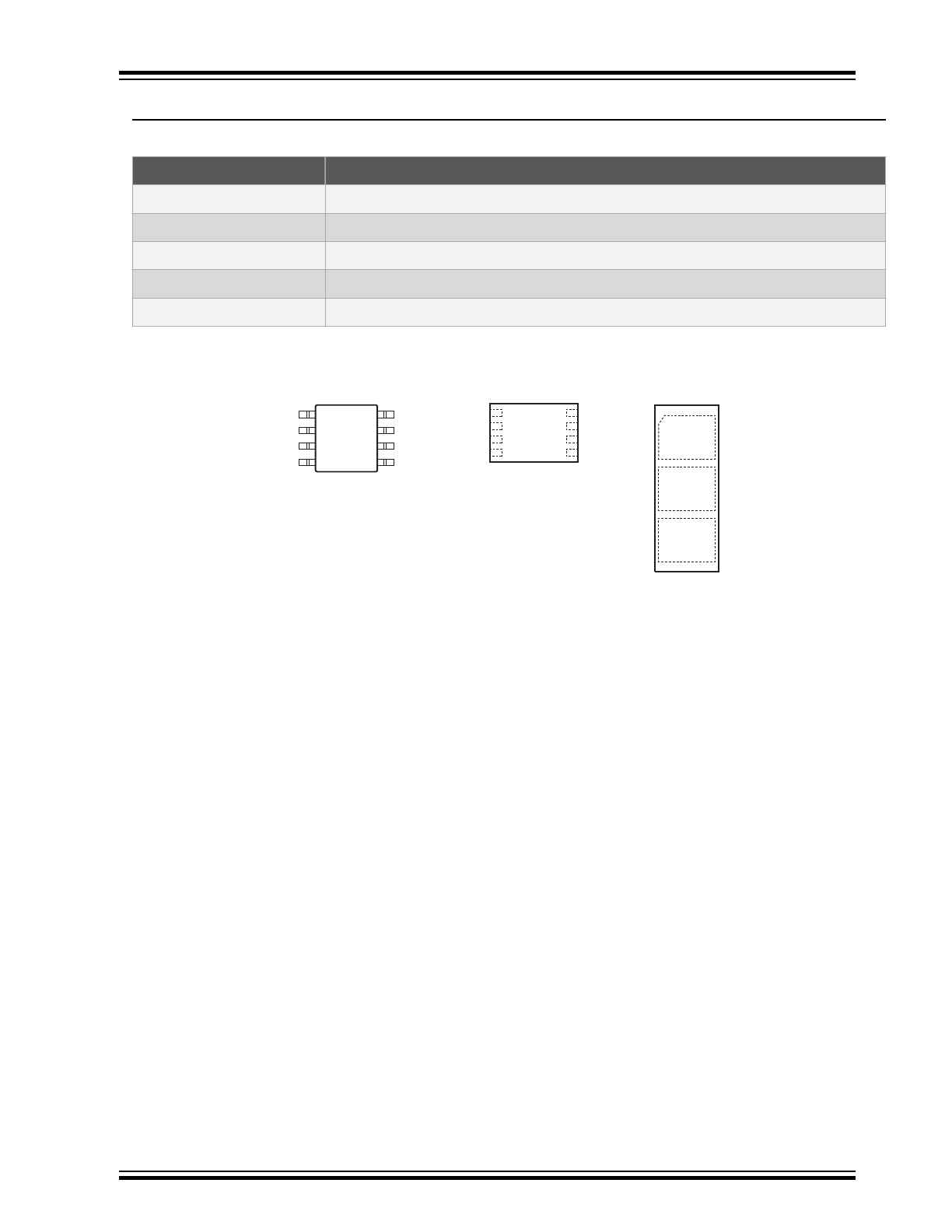
Package Types
Table 1. Pin Configuration
Pin
Function
NC
No Connect
GND
Ground
SDA
Serial Data
SCL
Serial Clock Input
VCC
Power Supply
Figure 1. Package Types
1
2
3
4
NC
NC
NC
GND
8
7
6
5
V
CC
NC
SCL
SDA
8-pad UDFN
(Top View)
1
2
3
4
NC
NC
NC
GND
8
7
6
5
V
CC
NC
SCL
SDA
8-lead SOIC
(Top View)
3-lead Contact
(Top View)
1
2
3
SDA
GND
V
CC
ATECC508A
©
2017 Microchip Technology Inc.
Datasheet Complete
DS20005927A-page 2

Table of Contents
Features.......................................................................................................................... 1
Applications..................................................................................................................... 1
Package Types................................................................................................................2
1. Introduction................................................................................................................7
1.1.
Applications.................................................................................................................................. 7
1.2.
Device Features........................................................................................................................... 7
1.3.
Cryptographic Operation.............................................................................................................. 8
1.4.
Commands................................................................................................................................... 9
2. Device Organization................................................................................................ 10
2.1.
EEPROM Data Zone.................................................................................................................. 10
2.1.1.
Certificate Storage....................................................................................................... 11
2.2.
EEPROM Configuration Zone.................................................................................................... 13
2.2.1.
SlotConfig (Bytes 20 to 51)..........................................................................................16
2.2.2.
Read Permissions........................................................................................................17
2.2.3.
Write Permissions........................................................................................................18
2.2.4.
Writing ECC Private Keys............................................................................................19
2.2.5.
KeyConfig (Bytes 96 through 127)...............................................................................19
2.2.6.
Special Memory Values in the Config Zone (Bytes 0 through 12)............................... 23
2.3.
EEPROM One Time Programmable (OTP) Zone.......................................................................23
2.4.
EEPROM Locking...................................................................................................................... 24
2.4.1.
Configuration Zone Locking.........................................................................................24
2.4.2.
Data and OTP Zone Locking....................................................................................... 24
2.4.3.
Individual Slot Locking................................................................................................. 25
2.5.
Static RAM (SRAM) Memory......................................................................................................26
2.5.1.
TempKey......................................................................................................................26
3. Security Information.................................................................................................28
3.1.
Cryptographic Standards............................................................................................................28
3.1.1.
SHA-256...................................................................................................................... 28
3.1.2.
HMAC/SHA-256...........................................................................................................28
3.1.3.
Elliptic Curve Digital Signature Algorithm (ECDSA).................................................... 28
3.1.4.
Elliptic Curve Diffie-Hellman (ECDH)...........................................................................28
3.2.
Key Uses and Restrictions......................................................................................................... 29
3.2.1.
Diversified Keys........................................................................................................... 29
3.2.2.
Rolled Keys..................................................................................................................29
3.2.3.
Created ECC Keys...................................................................................................... 29
3.2.4.
Created Secret Keys....................................................................................................30
3.2.5.
High Endurance Monotonic Counters..........................................................................30
3.2.6.
Limited Use Key (Slot 15 only).................................................................................... 30
3.2.7.
Password Checking..................................................................................................... 31
©
2017 Microchip Technology Inc.
Datasheet Complete
DS20005927A-page 3

3.2.8.
Transport Keys.............................................................................................................32
3.2.9.
Authorized Keys...........................................................................................................32
3.3.
Security Features....................................................................................................................... 33
3.3.1.
Physical Security......................................................................................................... 33
3.3.2.
Random Number Generator (RNG).............................................................................33
4. General I/O Information........................................................................................... 34
4.1.
Byte and Bit Ordering................................................................................................................. 34
4.1.1.
ECC Key Formatting....................................................................................................34
4.2.
Sharing the Interface.................................................................................................................. 35
5. Single-Wire Interface............................................................................................... 37
5.1.
I/O Tokens.................................................................................................................................. 37
5.2.
I/O Flags.....................................................................................................................................38
5.3.
Synchronization..........................................................................................................................38
5.3.1.
I/O Timeout.................................................................................................................. 38
5.3.2.
Synchronization Procedures........................................................................................39
6. I
2
C Interface.............................................................................................................40
6.1.
I/O Conditions.............................................................................................................................40
6.1.1.
Device is Asleep.......................................................................................................... 40
6.1.2.
Device is Awake.......................................................................................................... 40
6.2.
I
2
C Transmission to ATECC508A...............................................................................................42
6.2.1.
Word Address Values.................................................................................................. 42
6.2.2.
Command Completion Polling..................................................................................... 43
6.3.
Sleep Sequence......................................................................................................................... 43
6.4.
Idle Sequence............................................................................................................................ 43
6.5.
I
2
C Transmission from the ATECC508A.................................................................................... 44
6.6.
Address Counter........................................................................................................................ 44
6.7.
SMBus Timeout..........................................................................................................................45
6.8.
I
2
C Synchronization....................................................................................................................45
7. General Purpose I/O Pin......................................................................................... 47
8. Electrical Characteristics......................................................................................... 49
8.1.
Absolute Maximum Ratings........................................................................................................49
8.2.
Reliability.................................................................................................................................... 49
8.3.
AC Parameters: All I/O Interfaces.............................................................................................. 49
8.3.1.
AC Parameters: Single-Wire Interface.........................................................................50
8.3.2.
AC Parameters: I
2
C Interface...................................................................................... 52
8.4.
DC Parameters: All I/O Interfaces.............................................................................................. 53
8.4.1.
V
IH
and V
IL
Specifications............................................................................................53
9. Security Commands................................................................................................ 55
9.1.
I/O Groups..................................................................................................................................55
9.1.1.
Security Command Packets........................................................................................ 55
9.1.2.
Status/Error Codes...................................................................................................... 56
9.1.3.
Command Opcodes, Short Descriptions, and Execution Times..................................57
ATECC508A
©
2017 Microchip Technology Inc.
Datasheet Complete
DS20005927A-page 4

9.1.4.
Address Encoding........................................................................................................58
9.1.5.
Zone Encoding.............................................................................................................60
9.1.6.
Watchdog Fail-Safe..................................................................................................... 60
9.2.
CheckMac
Command...............................................................................................................61
9.3.
Counter
Command................................................................................................................. 62
9.4.
DeriveKey
Command............................................................................................................ 63
9.5.
ECDH
Command........................................................................................................................ 65
9.6.
GenDig
Command................................................................................................................... 66
9.7.
GenKey
Command................................................................................................................... 69
9.8.
HMAC
Command........................................................................................................................ 71
9.9.
Info
Command........................................................................................................................ 73
9.10.
Lock
Command........................................................................................................................ 74
9.11.
MAC
Command...........................................................................................................................76
9.12.
Nonce
Command......................................................................................................................77
9.13.
Pause
Command......................................................................................................................79
9.14.
PrivWrite
Command............................................................................................................ 79
9.15.
Random
Command................................................................................................................... 81
9.16.
Read
Command........................................................................................................................ 81
9.17.
SHA
Command...........................................................................................................................83
9.18.
Sign
Command........................................................................................................................ 84
9.19.
UpdateExtra
Command....................................................................................................... 86
9.20.
Verify
Command................................................................................................................... 87
9.21.
Write
Command......................................................................................................................90
9.21.1. Input Data Encryption.................................................................................................. 91
10. Compatibility............................................................................................................ 93
10.1. Microchip ATSHA204A...............................................................................................................93
10.2. Microchip ATECC108A...............................................................................................................93
11. Mechanical.............................................................................................................. 94
11.1. Wiring Configuration for Single-Wire Interface........................................................................... 94
12. Package Marking Information..................................................................................95
13. Package Drawings...................................................................................................96
13.1. 8-lead SOIC................................................................................................................................96
13.2. 8-pad UDFN............................................................................................................................... 99
13.3. 3-lead CONTACT..................................................................................................................... 102
14. Revision History.....................................................................................................104
The Microchip Web Site.............................................................................................. 105
Customer Change Notification Service........................................................................105
Customer Support....................................................................................................... 105
ATECC508A
©
2017 Microchip Technology Inc.
Datasheet Complete
DS20005927A-page 5

Product Identification System......................................................................................106
Microchip Devices Code Protection Feature............................................................... 107
Legal Notice.................................................................................................................107
Trademarks................................................................................................................. 107
Quality Management System Certified by DNV...........................................................108
Worldwide Sales and Service......................................................................................109
ATECC508A
©
2017 Microchip Technology Inc.
Datasheet Complete
DS20005927A-page 6

1.
Introduction
1.1
Applications
The ATECC508A device is a member of the Microchip CryptoAuthentication
™
family of crypto engine
authentication devices with highly secure hardware-based key storage.
The ATECC508A device has a flexible command set that allows use in many applications, including the
following:
•
Network/IoT Node Protection - Authenticates node IDs, ensures the integrity of messages, and
supports key agreement to create session keys for message encryption.
•
Anti-Counterfeiting - Validates that a removable, replaceable, or consumable client is authentic.
Examples of clients could be system accessories, electronic daughter cards, or other spare parts. It
can also be used to validate a software/firmware module or memory storage element.
•
Protecting Firmware or Media - Validates code stored in flash memory at boot to prevent
unauthorized modifications, encrypt downloaded program files as a common broadcast, or uniquely
encrypt code images to be usable on a single system only.
•
Storing Secure Data - Stores secret keys for use by crypto accelerators in standard
microprocessors. Programmable protection is available using encrypted/authenticated reads and
writes.
•
Checking User Password - Validates user-entered passwords without letting the expected value
become known, maps memorable passwords to a random number, and securely exchanges
password values with remote systems.
1.2
Device Features
The ATECC508A includes an EEPROM array which can be used for storage of up to 16 keys, certificates,
miscellaneous read/write, read-only or secret data, consumption logging, and security configurations.
Access to the various sections of memory can be restricted in a variety of ways and then the
configuration can be locked to prevent changes.
The ATECC508A features a wide array of defense mechanisms specifically designed to prevent physical
attacks on the device itself, or logical attacks on the data transmitted between the device and the
system(See Section
Security Features
). Hardware restrictions on the ways in which keys are used or
generated provide further defense against certain styles of attack(see Section
Key Uses and
Restrictions
).
Access to the device is made through a standard I
2
C Interface at speeds of up to 1 Mb/s(see Section
I
2
C
Interface
). The interface is compatible with standard Serial EEPROM I
2
C interface specifications. The
device also supports a Single-Wire Interface (SWI), which can reduce the number of GPIOs required on
the system processor, and/or reduce the number of pins on connectors(see Section
Single-Wire
Interface
). If the Single-Wire Interface is enabled, the remaining pin is available for use as a GPIO, an
authenticated output or tamper input(see Section
General Purpose I/O Pin
).
Using either the I
2
C or Single-Wire Interface, multiple ATECC508A devices can share the same bus,
which saves processor GPIO usage in systems with multiple clients such as different color ink tanks or
multiple spare parts, for example. See Sections
Sharing the Interface
and
Pause Command
for more
details regarding Single-Wire Interface implementation.
ATECC508A
Introduction
©
2017 Microchip Technology Inc.
Datasheet Complete
DS20005927A-page 7

Each ATECC508A ships with a guaranteed unique 72-bit serial number. Using the cryptographic
protocols supported by the device, a host system or remote server can verify a signature of the serial
number to prove that the serial number is authentic and not a copy. Serial numbers are often stored in a
standard Serial EEPROM; however, these can be easily copied with no way for the host to know if the
serial number is authentic or if it is a clone.
The ATECC508A can generate high-quality FIPS random numbers and employ them for any purpose,
including usage as part of the device’s crypto protocols. Because each random number is guaranteed to
be essentially unique from all numbers ever generated on this or any other device, their inclusion in the
protocol calculation ensures that replay attacks (i.e. re-transmitting a previously successful transaction)
will always fail(see Sections
Random Number Generator (RNG)
and
Random Command
).
System integration is easy due to a wide supply voltage range (of 2.0V to 5.5V) and an ultra-low sleep
current (of <150 nA). Complete DC parametrics are found in Section
Electrical Characteristics
. Multiple
package options are available (see Sections
Product Identification System
and
Package Drawings
).
See Section
Compatibility
for information regarding compatibility with the Microchip ATSHA204A and
ATECC108A devices.
1.3
Cryptographic Operation
The ATECC508A implements a complete asymmetric (public/private) key cryptographic signature solution
based upon Elliptic Curve Cryptography and the ECDSA signature protocol. The device features
hardware acceleration for the NIST standard P256 prime curve and supports the complete key life cycle
from high quality private key generation, to ECDSA signature generation, ECDH key agreement, and
ECDSA public key signature verification.
The hardware accelerator can implement such asymmetric cryptographic operations from ten to one-
thousand times faster than software running on standard microprocessors, without the usual high risk of
key exposure that is endemic to standard microprocessors.
The device is designed to securely store multiple private keys along with their associated public keys and
certificates. The signature verification command can use any stored or an external ECC public key. Public
keys stored within the device can be configured to require validation via a certificate chain to speed up
subsequent device authentications.
Random private key generation is supported internally within the device to ensure that the private key can
never be known outside of the device. The public key corresponding to a stored private key is always
returned when the key is generated and it may optionally be computed at a later time.
The ATECC508A also supports a standard hash-based challenge-response protocol in order to simplify
programming. In its most basic instantiation, the system sends a challenge to the device, which combines
that challenge with a secret key via the MAC, HMAC or SHA commands and then sends the response back
to the system. The device uses a SHA-256 cryptographic hash algorithm to make that combination so
that an observer on the bus cannot derive the value of the secret key, but preserving the ability of a
recipient to verify that the response is correct by performing the same calculation with a stored copy of
the secret on the recipient’s system.
Due to the flexible command set of the ATECC508A, these basic operation sets (i.e. ECDSA signatures,
ECDH key agreement and SHA-256 challenge-response) can be expanded in many ways. Using the
GenDig command(see Section
GenDig Command
), the values in other slots can be included in the
response digest or signature, which provides an effective way of proving that a data read really did come
from the device, as opposed to being inserted by a man-in-the-middle attacker. This same command can
ATECC508A
Introduction
©
2017 Microchip Technology Inc.
Datasheet Complete
DS20005927A-page 8

be used to combine two keys with the challenge, which is useful when there are multiple layers of
authentication to be performed.
In a host-client configuration where the host (for instance, a mobile phone) needs to verify a client (for
instance, an OEM battery), there is a need to store the secret in the host in order to validate the response
from the client. The CheckMac command(see Section
CheckMac Command
) allows the device to
securely store the secret in the host system and hides the correct response value from the pins, returning
only a yes or no answer to the system.
Finally, the hash combination of a challenge and secret key can be kept on the device and XORed with
the contents of a slot to implement an encrypted Read command(see Section
Read Command
), or it can
be XORed with encrypted input data to implement an encrypted Write command(see Section
Write
Command
).
All hashing functions are implemented using the industry-standard SHA-256 secure hash algorithm,
which is part of the latest set of high-security cryptographic algorithms recommended by various
government agencies and cryptographic experts(see Section
SHA-256
and Section
HMAC/SHA-256
).
The ATECC508A employs full-sized 256-bit secret keys to prevent any kind of exhaustive attack.
1.4
Commands
The ATECC508A is a command-based device which receives commands from the system, executes
those commands, and then returns a result or error code. Within this document, the following
nomenclature is used to describe the various commands:
•
Security Commands:
Described in Section
Security Commands
. This group of commands generally access the EEPROM
space and/or perform cryptographic computation. These commands are indicated with a special
font in this document (e.g. GenDig) and are available from all interfaces.
•
Cryptographic Commands:
This subset of the security commands includes all the ECC commands which access the hardware
ECC accelerator (GenKey, Sign, ECDH, and Verify) and the SHA commands which access the
hardware SHA accelerator (CheckMac, DeriveKey, GenDig, HMAC, MAC, SHA, and Nonce).
ATECC508A
Introduction
©
2017 Microchip Technology Inc.
Datasheet Complete
DS20005927A-page 9

2.
Device Organization
The ATECC508A contains an integrated EEPROM storage memory and SRAM buffer.
The EEPROM memory contains a total of 11,200 bits and is divided into the following zones:
Table 2-1. ATECC508A Zones
Zone
Description
Nomenclature
Data
Zone of 1,208 bytes (9.7 Kb) split into 16 general purpose read-only
or read/write memory slots of 36 bytes (288 bits), 72 bytes (576 bits),
or 416 bytes (3,328 bits) each that can be used to store keys (public
or private), signatures, certificates, calibration, model number, or
other information, typically that relate to the item to which the
ATECC508A device is attached. The access policy of each data slot
is determined by the values programmed into the corresponding
configuration values. However, the policies become effective upon
setting the LockValue byte only.
Slot<YY> = The entire
contents stored in Slot
YY of the Data zone.
Configuration
Zone of 128 bytes (1,024-bit) EEPROM that contains the serial
number and other ID information, as well as, access policy
information for each slot of the data memory. The values
programmed into the configuration zone will determine the access
policy of how each data slot will respond. The configuration zone can
be modified until it has been locked (LockConfig set to !
=0x55). In order to enable the access policies, the LockValue byte
must be set. (See section above)
SN<a:b> = A range of
bytes within a field of the
Configuration zone.
One Time
Programmable
(OTP)
Zone of 64 bytes (512 bits) of OTP bits. Prior to locking the OTP
zone, the bits may be freely written using the standard Write
command. The OTP zone can be used to store read-only data or
one-way fuse type consumption logging information.
OTP<bb> = A byte within
the OTP zone, while
OTP<aa:bb> indicates a
range of bytes.
Terms discussed within this document will have the following meanings:
Table 2-2. Document Terms
Term
Meaning
Block
A single 256-bit (32-byte) area of a particular memory zone. The industry SHA-256
documentation also uses the term “block” to indicate a 512-bit section of the message input.
Within this document, this convention is used only when describing hash input messages.
KeyID
KeyID is equivalent to the slot number for those slots designated to hold key values. Key 1 is
stored in Slot<1> and so on. While all 16 slots can potentially hold keys, those slots which are
configured to permit clear-text reads would not normally be used as private or secret keys by the
crypto commands.
param<b>
Indicates bit b of a command parameter or configuration byte.
SRAM
Contains input and output buffers, as well as state storage locations. See Section
Static RAM
(SRAM) Memory
.
2.1
EEPROM Data Zone
The data zone is broken into 16 slots, for which access restrictions are individually programmable. While
all slots can be used for private or secret keys or user data, only slots 8 through 15 are large enough to
ATECC508A
Device Organization
©
2017 Microchip Technology Inc.
Datasheet Complete
DS20005927A-page 10