
2017 Microchip Technology Inc.
DS20005882A-page 1
ATA663331/54
Features
• Supply Voltage up to 40V
• Operating Voltage V
VS
= 5V to 28V
• Supply Current
- Sleep Mode: Typically 10 μA
- Silent Mode: Typically 47 μA
- Very Low Current Consumption at Low
Supply Voltages (2V < V
VS
< 5.5V): Typically
130 μA
• Linear Low Drop Voltage Regulator, 85 mA
Current Capability:
- MLC (Multi-Layer Ceramic) Capacitor with
0Ω ESR
- Normal, Fail-Safe and Silent Mode
ATA663354: V
VCC
= 5.0V ± 2%
ATA663331: V
VCC
= 3.3V ± 2%
- Sleep Mode: VCC Is Switched Off
• VCC Undervoltage Detection with Open Drain
Reset Output (NRES, 4 ms Reset Time)
• Voltage Regulator Is Short Circuit and
Overtemperature Protected
• LIN Physical Layer According to LIN 2.0, 2.1, 2.2,
2.2A and SAEJ2602-2
• Bus Pin Is Overtemperature and Short Circuit
Protected versus GND and Battery
• Two Low Side Protected Switches and One High
Side Protected Switch
• Wake-Up Capability via LIN Bus (100 μs
Dominant) and WKin Pin
• Wake-Up Source Recognition
• TXD Time-Out Timer
• Advanced EMC and ESD Performance
• Fulfills the “OEM Hardware Requirements for LIN
in Automotive Applications”, Version.1.3
• Interference and Damage Protection According to
ISO7637
• Qualified According to AEC-Q100
• Available in 16-Pin, 3 mm x 5.5 mm VDFN
Package with Wettable Flanks (Moisture
Sensitivity Level 1)
Applications
• LIN Networks in Automotive
• Industrial
• Medical
• Consumer Applications
General Description
Designed in compliance with LIN specifications 2.0,
2.1, 2.2, 2.2A and SAEJ2602-2, the ATA6633XX is a
new generation of system basis chips with a fully
integrated LIN transceiver, a low drop voltage regulator
(3.3V/5V/85 mA), two low side drivers, and one high
side driver. This combination makes it possible to
develop simple, but powerful, slave nodes in LIN bus
systems. ATA6633XX is designed to handle low speed
data communication in vehicles (such as convenience
electronics). Improved slope control at the LIN driver
ensures secure data communication up to 20 kBaud.
The bus output is designed to withstand high voltage.
Sleep mode and Silent mode guarantee minimized
current consumption even in the case of a floating or
short circuited LIN bus.
Package Type
ATA663331/54
3 mm x 5.5 mm 16-Lead VDFN*
*Includes Exposed Thermal Pad (EP); see
Table 1-4
.
VCC
ATA663331
ATA663354
8DFN16
3 x 5.5
LIN
VS
GND
RXD
NRES
EN
TXD
WKin
LS2out
LS1out
HSout
WKout
LS2in
LS1in
HSin
LIN System Basis Chip Including LIN Transceiver, Voltage
Regulator, Dual Low Side Driver and a High Side Switch
ATA663331/54
DS20005882A-page 2
2017 Microchip Technology Inc.
Functional Block Diagram
13
GND
2
EN
4
TXD
1
RXD
VCC
16
NRES
3
HSout
9
Short
circuit and
overtemperature
protection
Voltage regulator
Normal/Silent/
Fail-
6afe Mode
5V
HS transistor driver
with short
circuit and
overtemperature
protection
Dual transistor driver
with short
circuit and
overtemperature
protection
Control
unit
Normal and
Fail-
6afe
Mode
RF-filter
LIN
VS
15
14
WKin
12
TXD
Time-out
timer
Slew rate control
Undervoltage reset
Sleep
mode
VCC
switched
off
Wake-up module
ATA663331/ATA663354
Receiver
9&&
-
+
9&&
5
WKout
8
HSin
6
LS1in
7
LS2in
LS1out
11
LS2out
10
WKin
LIN
9&&
2017 Microchip Technology Inc.
DS20005882A-page 3
ATA663331/54
1.0
FUNCTIONAL DESCRIPTION
1.1
Physical Layer Compatibility
Because the LIN physical layer is independent of
higher LIN layers (such as the LIN protocol layer), all
nodes with a LIN physical layer according to revision
2.x can be mixed with LIN physical layer nodes found
in older versions (LIN 1.0, LIN 1.1, LIN 1.2, LIN 1.3)
without any restrictions.
1.2
Operating Modes
FIGURE 1-1:
OPERATING MODES
1.2.1
NORMAL MODE
This is the normal transmitting and receiving mode of
the LIN Interface. Furthermore, the low side drivers can
only be operated in this mode. The VCC voltage
regulator works with 3.3V/5V output voltage. If an
undervoltage condition occurs, NRES is switched to
low and the IC changes its state to Fail-Safe mode.
EN = 1
EN = 0
“Go to sleep”
command
“Go to silent”
command
EN = 0
TXD = 0
b
c & f,
g & f
EN = 0
TXD = 0
EN = 0
TXD = 1
EN = 1
& f
EN = 1
& f
d,
e
c & f,
g & f,
d
b
a
b
& f
Fail-
6afe Mode
VCC: ON
VCC monitor active
Communication: OFF
Wake-up Signaling
Undervoltage Signaling
Normal Mode
VCC: ON
VCC monitor active
Communication: ON
Sleep Mode
VCC: OFF
Communication: OFF
Unpowered Mode
All circuitry OFF
Silent Mode
VCC: ON
VCC monitor active
Communication: OFF
a:
V
96
> V
VS_th_U_F_up
(2.4V)
b:
9
96
< V
VS_th_U_down
(1.9V)
c: Bus wake-up event (LIN)
d:
V
9&&
< V
9CC_th_uv_down
(4.2V)
e:
9
96
< V
VS_th_N_F_down
(3.9V)
f:
9
96
> V
VS_th_F_N_up
(4.9V)
g:
Local wake up (WKin)
& f
(1)
TXD = 1
& d & f
(1)
TABLE 1-1:
OPERATING MODES
Operating
Mode
Transceiver
Voltage
Regulator
Low Side
Outputs
High Side
Output
LIN
TXD
RXD
Fail-Safe
OFF
ON
OFF
HSin-
dependent
Recessive
Signaling fail-safe sources (see
Table 1-2
)
Normal
ON
ON
LSin-
dependent
HSin-
dependent
TXD-dependent
Follows data transmission
Silent
OFF
ON
OFF
HSin-
dependent
Recessive
High
High
Sleep/
Unpowered
OFF
OFF
OFF
OFF
Recessive
Low
Low
ATA663331/54
DS20005882A-page 4
2017 Microchip Technology Inc.
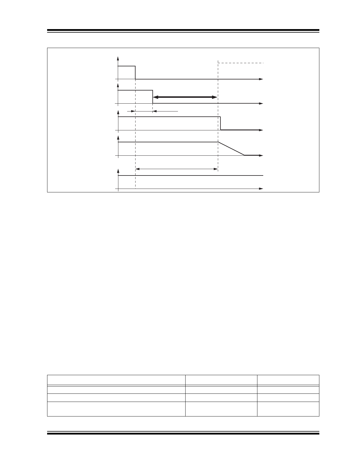
1.2.2
SILENT MODE
A falling edge at EN while TXD is high switches the IC
into Silent mode. The TXD signal has to be logic high
during the mode select window. See
Figure 1-2
.
The transmission path is disabled in Silent mode. The
voltage regulator is active. The overall supply current
from VBAT is a combination of the I
VSsilent
of typically
47 μA plus the VCC regulator output current I
VCC
.
FIGURE 1-2:
SWITCHING TO SILENT MODE
In Silent mode, the internal slave termination between
the LIN pin and VS pin is disabled to minimize the
current consumption in case the pin LIN is short-
circuited to GND. Only a weak pull up current (typically
10 μA) is present between the LIN pin and the VS pin.
The Silent mode can be activated regardless of the
current level on the LIN pin or WKin pin.
If an undervoltage condition occurs, NRES is switched
to low and the ATA6633XX changes its state to
Fail-Safe mode.
1.2.3
SLEEP MODE
A falling edge at EN while TXD is low switches the IC
into Sleep mode. The TXD signal has to be logic low
during the mode select window. See
Figure 1-3
.
Delay time silent mode
t
d_silent
= maximum 20
μs
Mode select window
LIN switches directly to recessive mode
t
d
= 3.2
μs
LIN
VCC
NRES
TXD
EN
Normal Mode
Silent Mode
2017 Microchip Technology Inc.
DS20005882A-page 5
ATA663331/54
FIGURE 1-3:
SWITCHING TO SLEEP MODE
In order to avoid any influence on the LIN pin while
switching to Sleep mode, it is possible to switch the EN
pin to low up to 3.2 μs earlier than the TXD pin. The
best and easiest way is to generate two simultaneous
falling edges at TXD and EN.
In Sleep mode, the transmission path is disabled.
Supply current from VBAT is typically I
VSsleep
= 10 μA.
The VCC regulator is switched off; NRES and RXD are
low. The internal slave termination between pin LIN and
pin VS is disabled to minimize the current consumption
in case pin LIN is short circuited to GND. Only a weak
pull-up current (typically 10 μA) between pin LIN and
pin VS is present. Sleep mode can be activated
independently from the current level on pin LIN. A
voltage less than the LIN pre-wake detection V
LINL
at
pin LIN activates the internal LIN receiver and starts the
wake-up detection timer.
If TXD is short circuited to GND, it is possible to switch
to Sleep mode via EN after t > t
dom
.
1.2.4
FAIL-SAFE MODE
The device automatically switches to Fail-Safe mode at
system power-up. The voltage regulator is switched on.
The NRES output remains low for t
res
= 4 ms and
resets the microcontroller. LIN communication is
switched off. The IC stays in this mode until EN is
switched to high. The IC then changes to Normal
mode. A low at NRES switches the IC directly into
Fail-Safe mode. During Fail-Safe mode, the TXD pin is
an output and signals the fail-safe source together with
the RXD output pin.
If the device enters Fail-Safe mode coming from the
Normal mode (EN = 1) due to a V
VS
undervoltage
condition (V
VS
< V
VS_th_N_F_down
), it is possible to
switch into Sleep or Silent mode through a falling edge
at the EN input. The current consumption can be
further reduced with this feature.
A wake-up event from either Silent or Sleep mode is
signaled to the microcontroller using the RXD pin and
the TXD pin. A V
VS
undervoltage condition is also
signaled at these two pins. The coding is shown in
Table 1-2
.
A wake-up event switches the IC to Fail-Safe mode.
Delay time sleep mode
t
d_sleep
= maximum 20
μs
LIN switches directly to recessive mode
t
d
= 3.2
μs
LIN
VCC
NRES
TXD
EN
Sleep Mode
Normal Mode
Mode select window
TABLE 1-2:
SIGNALING IN FAIL-SAFE MODE
Fail-Safe Sources
TXD
RXD
LIN wake-up (LIN pin)
Low
Low
Local wake-up (WKin pin)
Low
High
V
VS_th_N_F_down
(battery) undervoltage detection
(V
VS
< 3.9V)
High
Low
ATA663331/54
DS20005882A-page 6
2017 Microchip Technology Inc.
1.3
Wake-Up Scenarios from Silent
Mode or Sleep Mode
1.3.1
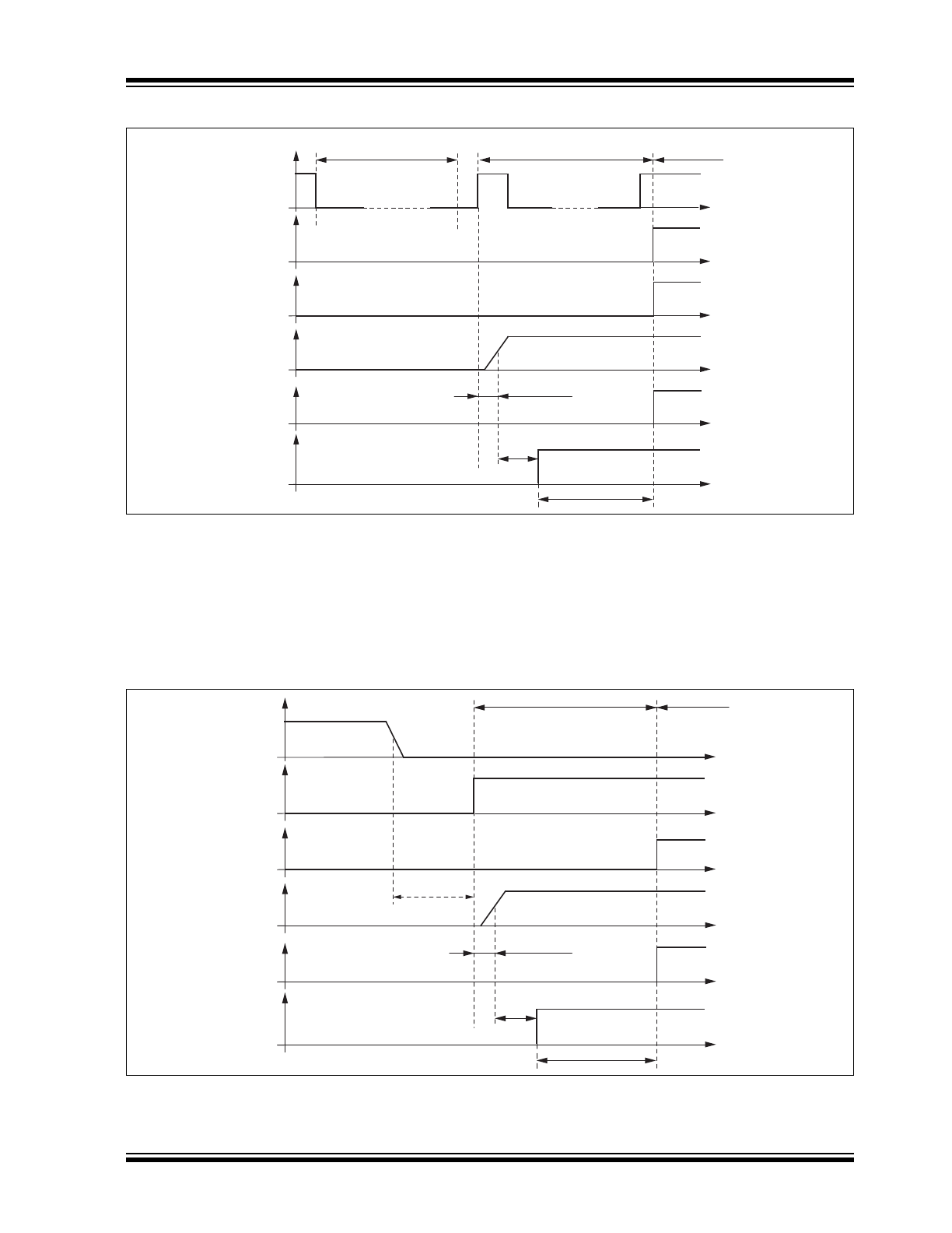
REMOTE WAKE-UP VIA LIN BUS
1.3.1.1
Remote Wake-up from Silent Mode
A remote wake-up from Silent mode is only possible if
TXD is high. A voltage less than the LIN pre-wake
detection V
LINL
at pin LIN activates the internal LIN
receiver and starts the wake-up detection timer. A falling
edge at the LIN pin followed by a dominant bus level
maintained for a certain period of time (> t
bus
) and the
following rising edge at pin LIN (see
Figure 1-4
) results
in a remote wake-up request. The device switches from
Silent mode to Fail-Safe mode, the VCC voltage
regulator remains activated and the internal LIN slave
termination resistor is switched on. The remote
wake-up request is indicated by a low level at the RXD
pin and TXD pin (strong pull down at TXD). EN high can
be used to switch directly to Normal mode.
FIGURE 1-4:
LIN WAKE-UP FROM SILENT MODE
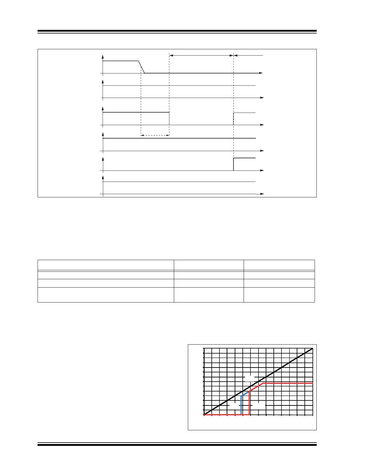
1.3.1.2
Remote Wake-Up from Sleep Mode
A voltage less than the LIN pre-wake detection V
LINL
at
the LIN pin activates the internal LIN receiver and starts
the wake-up detection timer.
A falling edge at the LIN pin followed by a dominant bus
level maintained for a certain period of time (> t
bus
) with
a subsequent rising edge at the LIN pin results in a
remote wake-up request. The device switches from
Sleep mode to Fail-Safe mode.
The VCC regulator is activated, and the internal LIN
slave termination resistor is switched on. The remote
wake-up request is indicated by a low level at RXD and
TXD (strong pull down at TXD). See
Figure 1-5
.
EN high can be used to switch directly from
Sleep/Silent mode to Normal mode. If EN is still high
after V
VCC
ramp-up and the undervoltage reset time,
the IC switches to Normal mode.
Undervoltage detection active
Low
Fail-
6afe Mode
Normal Mode
EN High
High
NRES
EN
VCC
RXD
LIN bus
Bus wake-up filtering time
t
bus
High
TXD
High
Low (strong pull-down)
2017 Microchip Technology Inc.
DS20005882A-page 7
ATA663331/54
FIGURE 1-5:
LIN WAKE-UP FROM SLEEP MODE
1.3.2
LOCAL WAKE-UP VIA WKin PIN
A falling edge at the WKin pin followed by a low level
maintained for a given time period (> t
WKin
) results in a
local wake-up request. The device switches to
Fail-Safe mode. The internal slave termination resistor
is switched on. The local wake-up request is indicated
by a low level at the TXD pin to generate an interrupt
for the microcontroller. When the WKin pin is low, it is
possible to switch to Silent mode or Sleep mode via the
EN pin. In this case, the wake-up signal has to be
switched to high > 10 μs before the negative edge at
WKin starts a new local wake-up request.
FIGURE 1-6:
LOCAL WAKE-UP FROM SLEEP MODE
t
VCC
Off state
On state
Low
Fail-
6afe Mode
Normal Mode
EN High
Microcontroller
start-up time delay
Reset
time
Low (strong pull
down)
Low
NRES
EN
VCC
RXD
LIN bus
Bus wake-up filtering time
t
bus
High
TXD
High
High
t
VCC
Off state
On state
High
Fail-
6afe Mode
Normal Mode
EN High
Microcontroller
start-up time delay
Reset
time
Low (strong pull
down)
Low
NRES
EN
VCC
RXD
WKin
TXD
Wake filtering time
t
WKin
State change
ATA663331/54
DS20005882A-page 8
2017 Microchip Technology Inc.
FIGURE 1-7:
LOCAL WAKE-UP FROM SILENT MODE
1.3.3
WAKE-UP SOURCE RECOGNITION
The device can distinguish between different wake-up
sources.
Table 1-3
. The wake-up source can be read
on the TXD and RXD pins in Fail-Safe mode. These
flags are immediately reset if the microcontroller sets
the EN pin to high and the IC is in Normal mode.
1.4
Behavior under Low Supply
Voltage Condition
After the battery voltage has been connected to the
application circuit, the voltage at the VS pin increases
according to the block capacitor (see
Typical
Application Circuit
). If V
VS
is higher than the minimum
VS operation threshold V
VS_th_U_F_up
,(typically 2.25V)
the IC mode changes from Unpowered mode to
Fail-Safe mode. As soon as V
VS
exceeds the
undervoltage threshold V
VS_th_F_N_up
(typically 4.6V),
the LIN transceiver and the dual low side switches can
be activated. The VCC output voltage reaches its
nominal value after t
VCC
. This parameter depends on
the externally applied VCC capacitor and the load. The
NRES output is low for the reset time delay t
reset
.
During this time t
reset
, no mode change is possible.
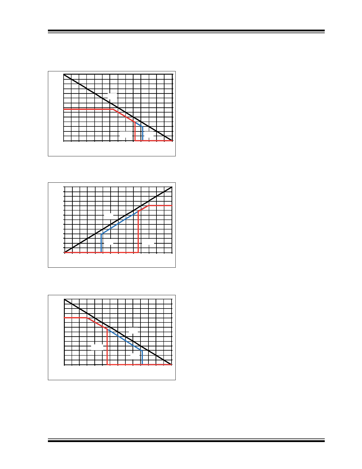
The behavior of VCC, NRES and VS is shown in
Figure 1-8
,
Figure 1-9
,
Figure 1-10
and
Figure 1-11
.
FIGURE 1-8:
VCC AND NRES VERSUS
VS (RAMP-UP) FOR 3.3V
Fail-
6afe Mode
Normal Mode
EN High
High
NRES
EN
VCC
RXD
WKin
TXD
Low (strong pull
down)
Wake filtering time
t
WKin
State change
TABLE 1-3:
SIGNALING IN FAIL-SAFE MODE
Fail-Safe Sources
TXD
RXD
Bus wake-up (LIN pin)
Low
Low
Local wake-up (WKin pin)
Low
High
V
VS_th_N_F_down
(battery) undervoltage detection
(V
VS
< 3.9V)
High
Low
V (V)
VS (V)
0.0
0.5
1.0
1.5
2.0
2.5
3.0
3.5
4.0
4.5
5.0
5.5
6.0
6.5
7.0
0.0
0.5
1.0
1.5
2.0
2.5
3.0
3.5
4.0
4.5
5.0
5.5
6.0
6.5
7.0
VS
VCC
NRES
2017 Microchip Technology Inc.
DS20005882A-page 9
ATA663331/54
FIGURE 1-9:
VCC AND NRES VERSUS
VS (RAMP-DOWN) FOR
3.3V
FIGURE 1-10:
VCC AND NRES VERSUS
VS (RAMP-UP) FOR 5V
FIGURE 1-11:
VCC AND NRES VERSUS
VS (RAMP-DOWN) FOR 5V
The graphs are only valid if the VS ramp-up and
ramp-down time is much slower than the VCC ramp-up
time t
VCC
and the NRES delay time t
reset
.
If during Sleep mode the voltage level of V
VS
drops
below the undervoltage detection threshold
V
VS_th_N_F_down
(typically 4.3V), the operation mode is
not changed and no wake-up is possible. Only if the
supply voltage on pin VS drops below the VS operation
threshold V
VS_th_U_down
(typically 2.05V), does the IC
switch to Unpowered mode.
If during Silent mode the VCC voltage drops below the
VCC undervoltage threshold V
VCC_th_uv_down
the IC
switches into Fail-Safe mode. If the supply voltage on
pin VS drops below the VS operation threshold
V
VS_th_U_down
(typically 2.05V), does the IC switch to
Unpowered mode.
If during Normal mode the voltage level on pin VS
drops below the VS undervoltage detection threshold
V
VS_th_N_F_down
(typically 4.3V), the IC switches to
Fail-Safe mode. This means the LIN transceiver and
the dual low side drivers are disabled in order to avoid
malfunctions or false bus messages. The voltage
regulator remains active.
• For ATA663331: In this undervoltage situation it is
possible to switch the device into Sleep mode or
Silent mode by a falling edge at the EN input. This
feature ensures that switching into these two
current saving modes is always possible, allowing
current consumption to be even further reduced.
When the VCC voltage drops below the VCC
undervoltage threshold V
VCC_th_uv_down
(typically
2.6V) the IC switches into Fail-Safe mode.
• For ATA663354: Because of the VCC
undervoltage condition in this situation, the IC is in
Fail-Safe mode and can be switched into Sleep
mode only. Only when the supply voltage V
VS
drops below the operation threshold
V
VS_th_U_down
(typically 2.05V) does the IC switch
into Unpowered mode.
The current consumption of the ATA6633XX in Silent
mode or in Fail-Safe mode is always below 170 μA,
even when the supply voltage V
VS
is lower than the
regulator’s nominal output voltage V
VCC
.
V (V)
VS (V)
0.0
0.5
1.0
1.5
2.0
2.5
3.0
3.5
4.0
4.5
5.0
5.5
6.0
6.5
7.0
0.0
0.5
1.0
1.5
2.0
2.5
3.0
3.5
4.0
4.5
5.0
5.5
6.0
6.5
7.0
VS
VCC
NRES
V (V)
VS (V)
0.0
0.5
1.0
1.5
2.0
2.5
3.0
3.5
4.0
4.5
5.0
5.5
6.0
6.5
7.0
0.0
0.5
1.0
1.5
2.0
2.5
3.0
3.5
4.0
4.5
5.0
5.5
6.0
6.5
7.0
VS
NRES
VCC
V (V)
VS (V)
0.0
0.5
1.0
1.5
2.0
2.5
3.0
3.5
4.0
4.5
5.0
5.5
6.0
6.5
7.0
0.0
0.5
1.0
1.5
2.0
2.5
3.0
3.5
4.0
4.5
5.0
5.5
6.0
6.5
7.0
VS
NRES
VCC
ATA663331/54
DS20005882A-page 10
2017 Microchip Technology Inc.
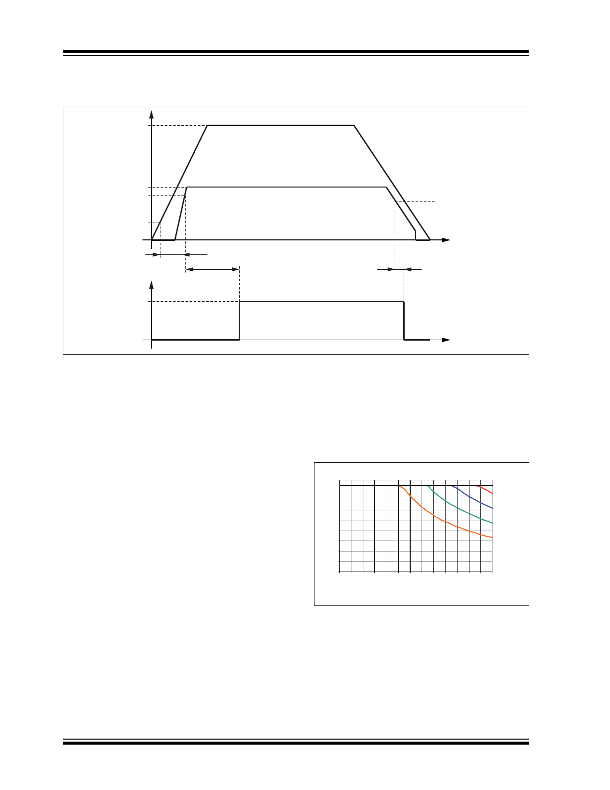
1.5
Voltage Regulator
FIGURE 1-12:
VOLTAGE REGULATOR: SUPPLY VOLTAGE RAMP-UP AND RAMP-DOWN
The voltage regulator needs an external capacitor for
compensation and to smooth the disturbances from the
microcontroller. It is recommended to use a MLC
capacitor with a minimum capacitance of 3.5 μF
together with a 100 nF ceramic capacitor. Depending
on the application, the values of these capacitors can
be modified by the customer.
When the ATA6633XX is being soldered onto the PCB,
it is mandatory to connect the exposed thermal pad
with a wide GND plate on the printed board to achieve
a good heat sink.
The main power dissipation of the IC is created from
the VCC output current I
VCC
, which is needed for the
application.
Figure 1-13
shows the safe operating area
of the ATA6633XX without considering any output
current of the drivers (LS1out, LS2out, HSout).
FIGURE 1-13:
POWER DISSIPATION:
SAFE OPERATING AREA:
REGULATOR’S OUTPUT
CURRENT I
VCC
VERSUS
SUPPLY VOLTAGE V
VS
AT
DIFFERENT AMBIENT
TEMPERATURES (R
thJA
=
45K/W ASSUMED)
VS
V
12V
3.3V/5.0V
V
VCC_th_uv_up
3.3V/5.0V
t
VCC
t
VCC
t
Reset
2.4V
t
res_f
NRES
t
V
VCC_th_uv_down
V
VS
[V]
I_Vcc [mA]
Tamb = 125°C
Tamb = 115°C
Tamb = 105°C
Tamb = 95°C
Tamb = 85°C
0
10
2 0
3 0
4 0
50
6 0
70
8 0
9 0
5
6
7
8
9
10
11
12
13
14
15
16
17
18