
2017 Microchip Technology Inc.
DS20005782B-page 1
ATA6565
Features
• Fully ISO 11898-2, ISO 11898-5,
ISO 11898-2: 2016 and SAE J2962-2 Compliant
• CAN FD Ready
• Communication Speed up to 5 Mbps
• Low Electromagnetic Emission (EME) and High
Electromagnetic Immunity (EMI)
• Differential Receiver with Wide Common-Mode
Range
• Remote Wake-up Capability via CAN Bus –
Wake-up on Pattern (WUP) as Specified in
ISO 11898-2: 2016, 3.8 µs Activity Filter Time
• Functional Behavior Predictable Under All Supply
Conditions
• Transceiver Disengages from the Bus when Not
Powered Up
• RXD Recessive Clamping Detection
• High Electrostatic Discharge (ESD) Handling
Capability on the Bus Pins
• Bus Pins Protected Against Transients in
Automotive Environments
• Transmit Data (TXD) Dominant Time-out Function
• Undervoltage Detection on VCC Pin
• Bus Pins Short-Circuit and Overtemperature
Protected
• Fulfills the OEM “Hardware Requirements for LIN,
CAN and FlexRay™ Interfaces in Automotive
Applications”
, Rev. 1.3
• Qualified According to AEC-Q100
• Two Ambient Temperature Grades Available:
- ATA6565-GCQW1 and ATA6565-GNQW1 up
to T
amb
= +125°C
- ATA6565-GCQW0 and ATA6565-GNQW0 up
to T
amb
= +150°C
• 14-Lead SOIC Package and 14-Lead VDFN
Package with Wettable Flanks (Moisture
Sensitivity Level 1)
Applications
Classical CAN and CAN FD networks in Automotive,
Industrial, Aerospace, Medical and Consumer
applications.
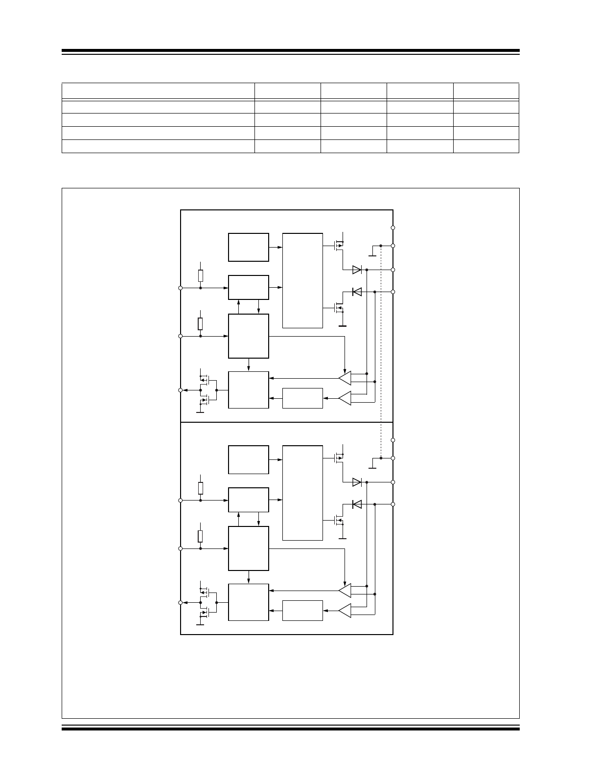
General Description
The ATA6565 is a fully integrated, dual high-speed CAN
transceiver with two completely independent and
separated high-speed CAN transceivers integrated in
one package (only the GND pins, GND1 and GND2, are
internally connected). Each of the two identical
transceivers provides an interface between a Controller
Area Network (CAN) protocol controller and a physical
two-wire CAN bus.
The device is designed for high-speed (up to 5 Mbps)
CAN applications in the automotive industry, providing
differential transmit and receive capability to (a micro-
controller with) a CAN protocol controller. It offers
improved Electromagnetic Compatibility (EMC) and
Electrostatic Discharge (ESD) performance, as well as
features such as:
• Ideal passive behavior to the CAN bus when the
supply voltage is off
• Very low current consumption in Standby mode
with bus wake-up capability
Two operating modes, together with the dedicated
fail-safe features, make the ATA6565 an excellent choice
for all types of high-speed CAN networks. The ATA6565
includes more than one high-speed CAN interface which
requires a Low-Power mode with wake-up capability via
the CAN bus. These features are especially valuable for
body control units and gateways.
Package Types
1
2
3
4
5
6
7
TXD
GND
VCC
RXD
VIO
MISO
INH
NCS
CANH
CANL
MOSI
VS
WAKE
SCK
14
13
12
11
10
9
8
ATA6565
ATA6565
14-Pin SOIC
ATA6565
3 x 4.5 mm
14-Pin VDFN
1
2
3
4
5
6
7
14
13
12
11
10
9
8
ATA6565
TXD1
GND1
VCC1
RXD1
TXD2
GND2
VCC2
STBY1
CANH1
CANL1
STBY2
CANH2
CANL2
RXD2
TXD1
GND1
VCC1
RXD1
TXD2
GND2
VCC2
STBY1
CANH1
CANL1
STBY2
CANH2
CANL2
RXD2
Dual High-Speed CAN Transceiver with Standby Mode
ATA6565
DS20005782B-page 2
2017 Microchip Technology Inc.
ATA6565 Family Members
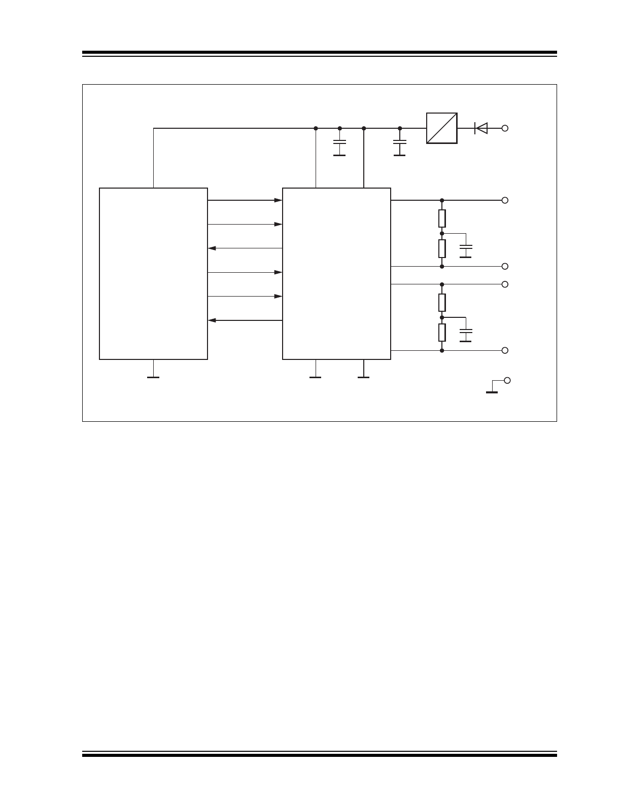
Block Diagram
Device
Grade 0
Grade 1
SOIC14
VDFN14
ATA6565-GNQW1
X
X
ATA6565-GNQW0
X
X
ATA6565-GCQW1
X
X
ATA6565-GCQW0
X
X
Note:
For ordering information, see the
“Product Identification System”
section.
Temperature
Protection
Control
Unit
Wake-up
Filter
Slope
Control
and
Driver
TXD
Time-out
Timer
V
&&
HSC
(1)
WUC
(2)
V
&&
V
&&
V
&&
MUX
1
TXD1
STBY1
CANH1
RXD1
14
13
4
GND1
(3)
Transceiver 1
2
CANL1
12
9&&
Temperature
Protection
Control
Unit
Wake-up
Filter
Slope
Control
and
Driver
TXD
Time-out
Timer
VCC2
HSC
(1)
WUC
(2)
VCC2
VCC2
VCC2
MUX
5
TXD2
STBY2
CANH2
RXD2
11
10
8
GND2
(3)
Transceiver 2
6
CANL2
9
V
&&
7
Note 1:
HSC: High-Speed Comparator.
2:
WUC: Wake-up Comparator.
3:
GND1 and GND2 are internally connected.
2017 Microchip Technology Inc.
DS20005782B-page 3
ATA6565
1.0
FUNCTIONAL DESCRIPTION
The ATA6565 is a stand-alone, dual high-speed CAN
transceiver, compliant with the ISO 11898-2, ISO
11898-5, ISO 11898-2: 2016 and SAE J2962-2 stan-
dards. Each of the two transceivers provides a very low
current consumption in Standby mode and wake-up
capability via the CAN bus.
The functions described in the following text apply to
each of the two identical high-speed CAN transceivers
integrated in the ATA6565. Therefore, if for example,
the CANH pin is stated, this applies to each of the two
transceivers, meaning CANH1 and CANH2. The two
transceivers are identical and there is no internal
connection between them (with the exception of the
GND pins, GND1 and GND2), so they work completely
independently.
1.1
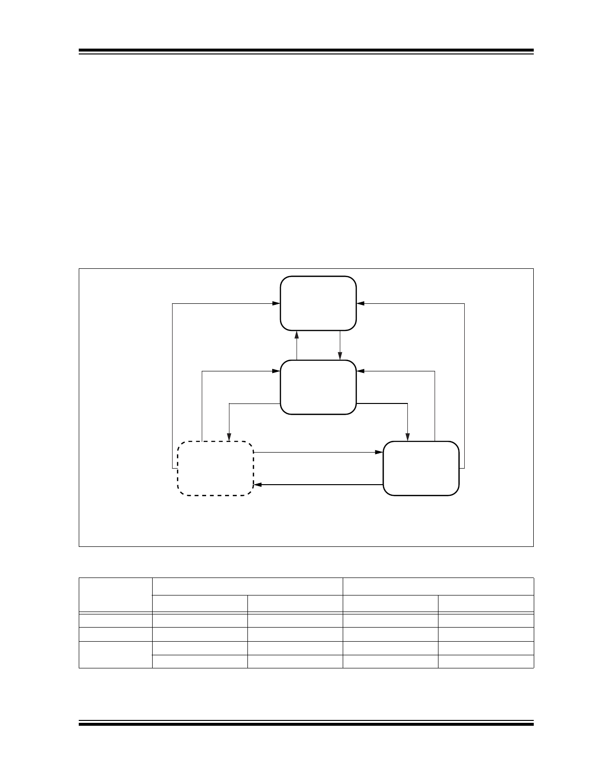
Operating Modes
Each of the transceivers supports three operating
modes: Unpowered, Standby and Normal. Additionally,
there is the internal Silent mode, which is not externally
accessible. This mode is a Receive Only mode, which
means the CAN drivers are deactivated and only data
from the bus can be received.
The operating modes can be selected via the STBY
pins (STBY1 and STBY2). See
Figure 1-1
and
Table 1-1
for a description of the operating modes.
FIGURE 1-1:
OPERATING MODES
STBY =
0 and
TXD =
0
V
CC
< V
uvd(VCC)
STBY =
1
STBY =
0 and
TXD =
1 and
Error =
0 and
TXD =
1
*
Error =
1
Error =
0
V
CC
< V
uvd(V
&&)
V
CC
< V
uvd
9&&
V
CC
> V
uvd9&&
Unpowered
Mode
Standby
Mode
Silent
Mode
Normal
Mode
STBY =
1
* Silent mode is externally not accessible. In this mode, the transceiver can only receive data from the bus,
but the transmitter is disabled.
TABLE 1-1:
OPERATING MODES
Mode
Inputs
Outputs
STBY
Pin TXD
CAN Driver
Pin RXD
Unpowered
X
(
1
)
X
(
1
)
Recessive
Recessive
Standby
High
X
(
1
)
Recessive
Active
(
2
)
Normal
Low
Low
Dominant
Low
Low
High
Recessive
High
Note 1:
Irrelevant.
2:
Reflects the bus only for wake-up.
ATA6565
DS20005782B-page 4
2017 Microchip Technology Inc.
1.1.1
NORMAL MODE
A low level on the STBY pin, together with a high level on
the TXD pin, selects the Normal mode. In this mode, the
transceiver is able to transmit and receive data via the
CANH and CANL bus lines (see the
Block Diagram
).
The output driver stage is active and drives data from the
TXD input to the CAN bus. The High-Speed Comparator
(HSC) converts the analog data on the bus lines into
digital data, which is output to pin RXD. The bus biasing
is set to V
VCC
/2 and the undervoltage monitoring of V
VCC
is active.
The slope of the output signals on the bus lines is con-
trolled and optimized in a way that ensures the lowest
possible Electromagnetic Emission (EME).
To switch the device to Normal Operating mode, set the
STBY pin to low and the TXD pin to high (see
Table 1-1
and
Figure 1-2
). The STBY pin provides a pull-up
resistor to VCC, thus ensuring a defined level if the pin
is open.
Please note that the device cannot enter Normal mode
as long as TXD is at ground level.
The switching into Normal mode is depicted in
Figure 1-2
.
FIGURE 1-2:
SWITCHING FROM STANDBY MODE TO NORMAL MODE
STBY
TXD
Standby Mode
t
del(stby-norm)
=
47 μs max
Normal Mode
t
t
t
Operation
Mode
2017 Microchip Technology Inc.
DS20005782B-page 5
ATA6565
1.1.2
STANDBY MODE
A high level on the STBY pin selects Standby mode. In
this mode, the transceiver is not able to transmit or
correctly receive data via the bus lines. The transmitter
and the High-Speed Comparator (HSC) are switched off
to reduce current consumption.
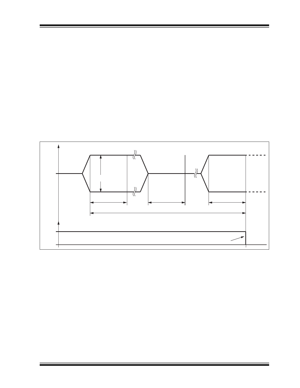
1.1.2.1
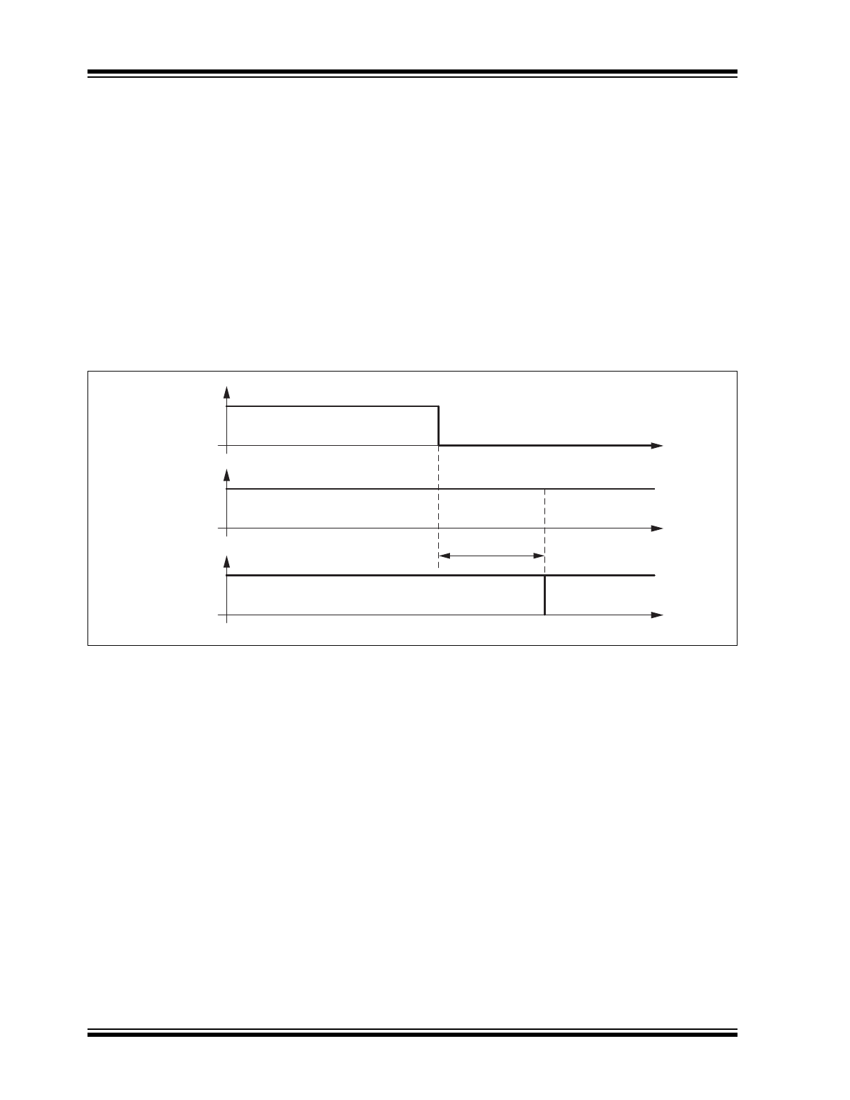
Remote Wake-up via the CAN Bus
In Standby mode, the bus lines are biased to ground to
reduce current consumption to a minimum. The device
monitors the bus lines for a valid wake-up pattern, as
specified in the ISO 11898-2: 2016. This filtering helps
to avoid spurious wake-up events which would be
triggered by scenarios, such as a dominant clamped
bus or by a dominant phase due to noise, spikes on the
bus, automotive transients or EMI.
The wake-up pattern consists of at least two consecu-
tive dominant bus levels for a duration of at least t
Filter
,
each separated by a recessive bus level with a duration
of at least t
Filter
. Dominant or recessive bus levels
shorter than t
Filter
are always ignored. The complete
dominant-recessive-dominant pattern, as shown in
Figure 1-3
, must be received within the bus wake-up
time-out time, t
Wake
, to be recognized as a valid
wake-up pattern. Otherwise, the internal wake-up logic
is reset and then the complete wake-up pattern must
be retransmitted to trigger a wake-up event. The RXD
pin remains at a high level until a valid wake-up event
has been detected.
During Normal mode, at a VCC undervoltage condition
or when the complete wake-up pattern is not received
within t
Wake
, no wake-up is signaled at the RXD pin.
FIGURE 1-3:
TIMING OF THE BUS WAKE-UP PATTERN (WUP) IN STANDBY MODE
When a valid CAN wake-up pattern is detected on the
bus, the RXD pin switches to low to signal a wake-up
request. A transition to Normal mode is not triggered
until the STBY pin is forced back to low by the
microcontroller.
1.2
Fail-Safe Features
1.2.1
TXD DOMINANT TIME-OUT
FUNCTION
A TXD dominant time-out timer is started when the TXD
pin is set to low. If the low state on the TXD pin persists
for longer than t
to(dom)TXD
, the transmitter is disabled,
releasing the bus lines to the recessive state. This func-
tion prevents a hardware and/or software application
failure from driving the bus lines to a permanent domi-
nant state (blocking all network communications). The
TXD dominant time-out timer is reset when the TXD pin
is set to high. If the low state on the TXD pin was longer
than t
to(dom)TXD
, then the TXD pin has to be set to high
≥ 4 µs in order to reset the TXD dominant time-out timer.
1.2.2
INTERNAL PULL-UP STRUCTURE
AT THE TXD AND STBY INPUT PINS
The TXD and STBY pins have an internal pull-up to
VCC. This ensures a safe, defined state in case one or
both pins are left floating. Pull-up currents flow in these
pins in all states, meaning all pins should be in a high
state during Standby mode to minimize the current
consumption.
1.2.3
UNDERVOLTAGE DETECTION ON
PIN VCC
If V
VCC
drops below its undervoltage detection level,
V
uvd(VCC)
(see
Section 2.0 “Electrical Characteris-
tics”
), the transceiver switches off and disengages from
the bus until V
VCC
has recovered. The low-power
t
dom
= t
)LOWHU
V
Diff
t
dom
= t
)LOWHU
t
rec
= t
)LOWHU
WW
:DNH
dominant
recessive
Bus Wake-up
is Signaled
CANH
CANL
RXD
dominant
ATA6565
DS20005782B-page 6
2017 Microchip Technology Inc.
wake-up comparator is only switched off during a VCC
undervoltage. The logic state of the STBY pin is ignored
until the VCC voltage has recovered.
1.2.4
BUS WAKE-UP ONLY AT
DEDICATED WAKE-UP PATTERN
Due to the implementation of the wake-up filtering, the
transceiver does not wake-up when the bus is in a long
dominant phase; it only wakes up at a dedicated wake-up
pattern, as specified in the ISO 11898-2: 2016. This
means for a valid wake-up, at least two consecutive
dominant bus levels for a duration of at least, t
Filter
, each
separated by a recessive bus level with a duration of at
least, t
Filter
, must be received via the bus. Dominant or
recessive bus levels shorter than t
Filter
are always
ignored. The complete dominant-recessive-dominant
pattern, as shown in
Figure 1-3
, must be received within
the bus wake-up time-out time, t
Wake
, to be recognized
as a valid wake-up pattern. This filtering leads to a higher
robustness against EMI and transients, and therefore,
significantly reduces the risk of an unwanted bus
wake-up.
1.2.5
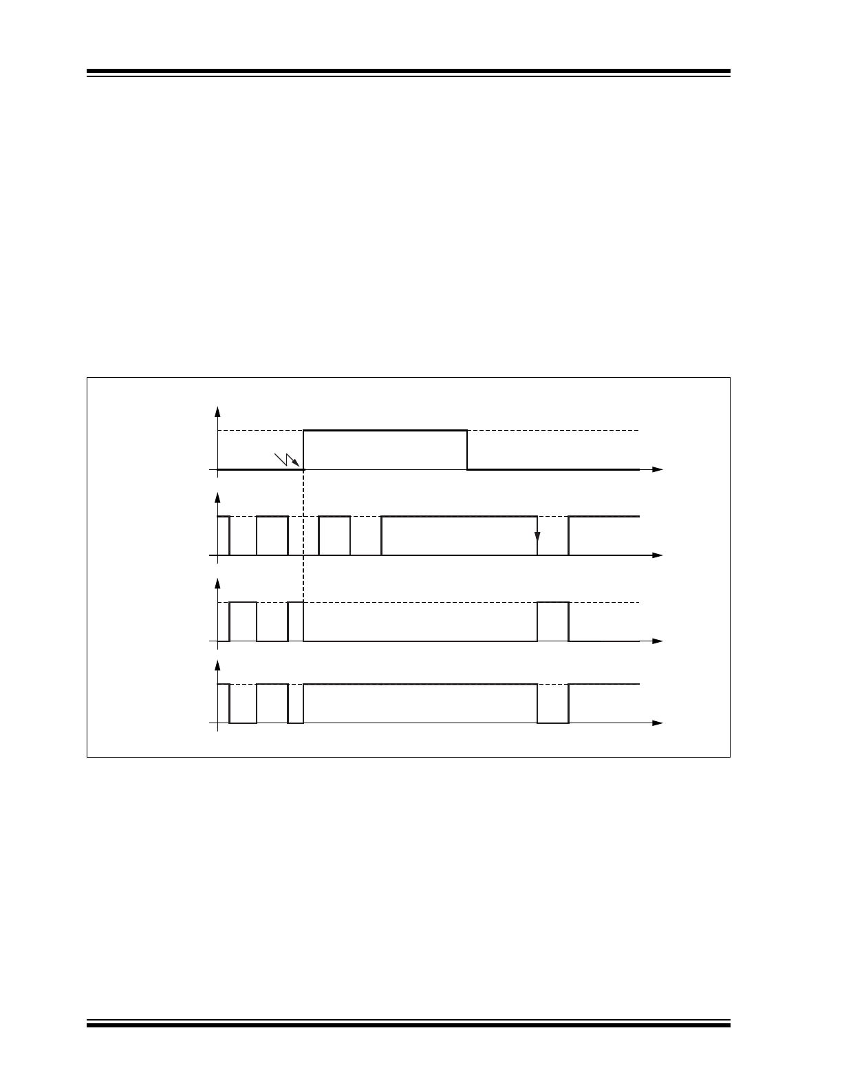
OVERTEMPERATURE
PROTECTION
The output drivers are protected against overtemperature
conditions. If the junction temperature exceeds the shut-
down junction temperature, T
Jsd
, the output drivers are
disabled until the junction temperature drops below T
Jsd
and pin TXD is at a high level again. This TXD condition
ensures that output driver oscillations, due to temperature
drift, are avoided.
FIGURE 1-4:
RELEASE OF TRANSMISSION AFTER OVERTEMPERATURE CONDITION
Failure
Overtemp
GND
TXD
Overtemperature
R
D
R
t
t
t
OT
BUS V
DIFF
(CANH-CANL)
V
VCC
R
D
D
t
RXD
V
VCC
GND
2017 Microchip Technology Inc.
DS20005782B-page 7
ATA6565
1.2.6
SHORT-CIRCUIT PROTECTION OF
THE BUS PINS
The CANH and CANL bus outputs are short-circuit
protected, either against GND or a positive supply volt-
age. A current-limiting circuit protects the transceiver
against damage. If the device is heating up due to a
continuous short on CANH or CANL, the internal
overtemperature protection switches the bus transmitter
off.
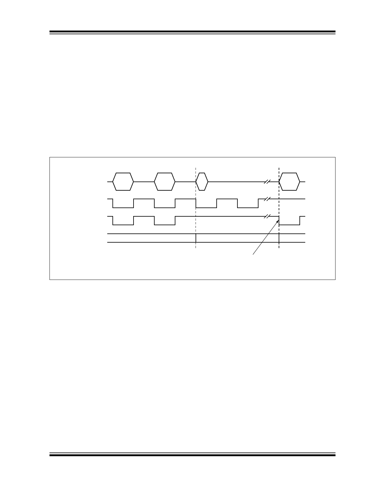
1.2.7
RXD RECESSIVE CLAMPING
This fail-safe feature prevents the controller from sending
data on the bus if its RXD is clamped to high (e.g., reces-
sive). That is, if the RXD pin cannot signalize a dominant
bus condition (e.g., because it is shorted to VCC), the
transmitter is disabled to avoid possible data collisions on
the bus. In Normal mode, the device permanently com-
pares the state of the High-Speed Comparator (HSC)
with the state of the RXD pin. If the HSC indicates a
dominant bus state for more than t
RC_det
, without the
RXD pin doing the same, a recessive clamping situation
is detected and the transceiver is forced into Silent mode.
This Fail-Safe mode is released by either entering
Standby or Unpowered mode, or if the RXD pin is
showing a dominant (e.g., low) level again.
FIGURE 1-5:
RXD RECESSIVE CLAMPING DETECTION
CAN
TXD
RXD
Operation
Mode
Normal
Normal
Silent
If the clamping condition is removed and a
dominant bus is detected, the transceiver
goes back to normal mode.
If the clamping condition is removed and a
dominant bus is detected, the transceiver
goes back to Normal mode.

ATA6565
DS20005782B-page 8
2017 Microchip Technology Inc.
1.3
Pin Description
The descriptions of the pins are listed in
Table 1-2
.
TABLE 1-2:
PIN FUNCTION TABLE
Pin Number
Pin Name
Description
1
TXD1
Transmit Data Input 1
2
GND1
Ground 1, Internally Connected to GND2
3
VCC1
Supply Voltage of Transceiver 1
4
RXD1
Receive Data Output 1; Reads out Data from the Bus Lines of Transceiver 1
5
TXD2
Transmit Data Input 2
6
GND2
Ground 2, Internally Connected to GND1
7
VCC2
Supply Voltage of Transceiver 2
8
RXD2
Receive Data Output 2; Reads out Data from the Bus Lines of Transceiver 2
9
CANL2
Low-Level CAN Bus Line 2
10
CANH2
High-Level CAN Bus Line 2
11
STBY2
Standby Mode Control Input of Transceiver 2
12
CANL1
Low-Level CAN Bus Line 1
13
CANH1
High-Level CAN Bus Line 1
14
STBY1
Standby Mode Control Input of Transceiver 1
15
EP
(
1
)
Exposed Thermal Pad: Heat Slug, Internally Connected to the GND Pins
Note 1:
Only for the VDFN package
2017 Microchip Technology Inc.
DS20005782B-page 9
ATA6565
Typical Application
13
14
1
11
2
3
6
CANH1
V
&&
7
V
CC2
100 nF
22 μF
(1)
V
DD
Microcontroller
GND
ATA6565
CANH1
STBY1
TXD1
4
5
8
RXD1
RXD2
TXD2
STBY2
CANL1
V
BAT
+
12
10
9
CANL1
GND1
(2)
GND2
(2)
CANH2
CANH2
CANL2
CANL2
GND
5V
12V

ATA6565
DS20005782B-page 10
2017 Microchip Technology Inc.
NOTES: