
2017 Microchip Technology Inc.
DS20005790B-page 1
ATA6562/3
Features
• Fully ISO 11898-2, ISO 11898-2: 2016 and
SAE J2962-2 Compliant
• CAN FD Ready
• Communication Speed up to 5 Mbps
• Low Electromagnetic Emission (EME) and High
Electromagnetic Immunity (EMI)
• Differential Receiver with Wide Common Mode
Range
• ATA6562: Silent Mode
• Remote Wake-Up Capability via CAN Bus -
Wake-Up on Pattern (WUP), as Specified in
ISO 11898-2: 2016, 3.8 µs Activity Filter Time
• Functional Behavior Predictable under All Supply
Conditions
• Transceiver Disengages from the Bus When Not
Powered Up
• RXD Recessive Clamping Detection
• High Electrostatic Discharge (ESD) Handling
Capability on the Bus Pins
• Bus Pins Protected Against Transients in
Automotive Environments
• Transmit Data (TXD) Dominant Time-Out
Function
• Undervoltage Detection on VCC and VIO Pins
• CANH/CANL Short-Circuit and Overtemperature
Protected
• Fulfills the OEM “Hardware Requirements for LIN,
CAN and FlexRay Interfaces in Automotive Appli-
cations, Rev. 1.3"
• Qualified According to AEC-Q100
• Two Ambient Temperature Grades Available:
- ATA6562-GAQW1, ATA6563-GAQW1,
ATA6562-GBQW1 and ATA6563-GBQW1 up
to T
amb
= +125°C
- ATA6562-GAQW0, ATA6563-GAQW0,
ATA6562-GBQW0 and ATA6563-GBQW0 up
to T
amb
= +150°C
• Packages: SOIC8, VDFN8 with Wettable Flanks
(Moisture Sensitivity Level 1)
Applications
Classical CAN and CAN FD networks in Automotive,
Industrial, Aerospace, Medical and Consumer
applications.
General Description
The ATA6562/ATA6563 is a high-speed CAN
transceiver that provides an interface between a
controller area network (CAN) protocol controller and
the physical two-wire CAN bus.
The transceiver is designed for high-speed (up to
5 Mbps) CAN applications in the automotive industry,
providing differential transmit and receive capability to
(a microcontroller with) a CAN protocol controller. It
offers improved electromagnetic compatibility (EMC)
and electrostatic discharge (ESD) performance, as well
as features such as:
• Ideal passive behavior to the CAN bus when the
supply voltage is off
• Direct interfacing to microcontrollers with supply
voltages from 3V to 5V (ATA6563)
Three operating modes together with the dedicated
fail-safe features make the ATA6562/ATA6563 an
excellent choice for all types of high-speed CAN
networks, especially in nodes requiring low-power
mode with wake-up capability via the CAN bus.
Package Types
ATA6563
3 x 3 VDFN* with
wettable flanks
ATA6562
SOIC
VCC
GND
RXD
CANH
CANL
1
2
3
4
8
7
6
5 NSIL
STBY
TXD
ATA6563
SOIC
VCC
GND
RXD
CANH
CANL
1
2
3
4
8
7
6
5 VIO
STBY
TXD
ATA6562
3 x 3 VDFN* with
wettable flanks
VCC
GND
RXD
CANH
CANL
NSIL
STBY
TXD
1
2
3
4
8
7
6
5
*Includes Exposed Thermal Pad (EP); see
Table 1-2
.
VCC
GND
RXD
CANH
CANL
VIO
STBY
TXD
1
2
3
4
8
7
6
5
High-Speed CAN Transceiver with Standby Mode
ATA6562/3
DS20005790B-page 2
2017 Microchip Technology Inc.
ATA6562/ATA6563 Family Members
Device
VIO Pin
NSIL
Grade 0
Grade 1
VDFN8
SOIC8
Description
ATA6562-GAQW0
X
X
X
Standby mode and Silent mode
ATA6562-GAQW1
X
X
X
Standby mode and Silent mode
ATA6562-GBQW0
X
X
X
Standby mode and Silent mode
ATA6562-GBQW1
X
X
X
Standby mode and Silent mode
ATA6563-GAQW0
X
X
X
Standby mode, VIO - pin for
compatibility with 3.3V and 5V
microcontroller
ATA6563-GAQW1
X
X
X
Standby mode, VIO - pin for
compatibility with 3.3V and 5V
microcontroller
ATA6563-GBQW0
X
X
X
Standby mode, VIO-pin for
compatibility with 3.3V and 5V
microcontroller
ATA6563-GBQW1
X
X
X
Standby mode, VIO - pin for
compatibility with 3.3V and 5V
microcontroller
Note:
For ordering information, see the
Product Identification System
section.
2017 Microchip Technology Inc.
DS20005790B-page 3
ATA6562/3
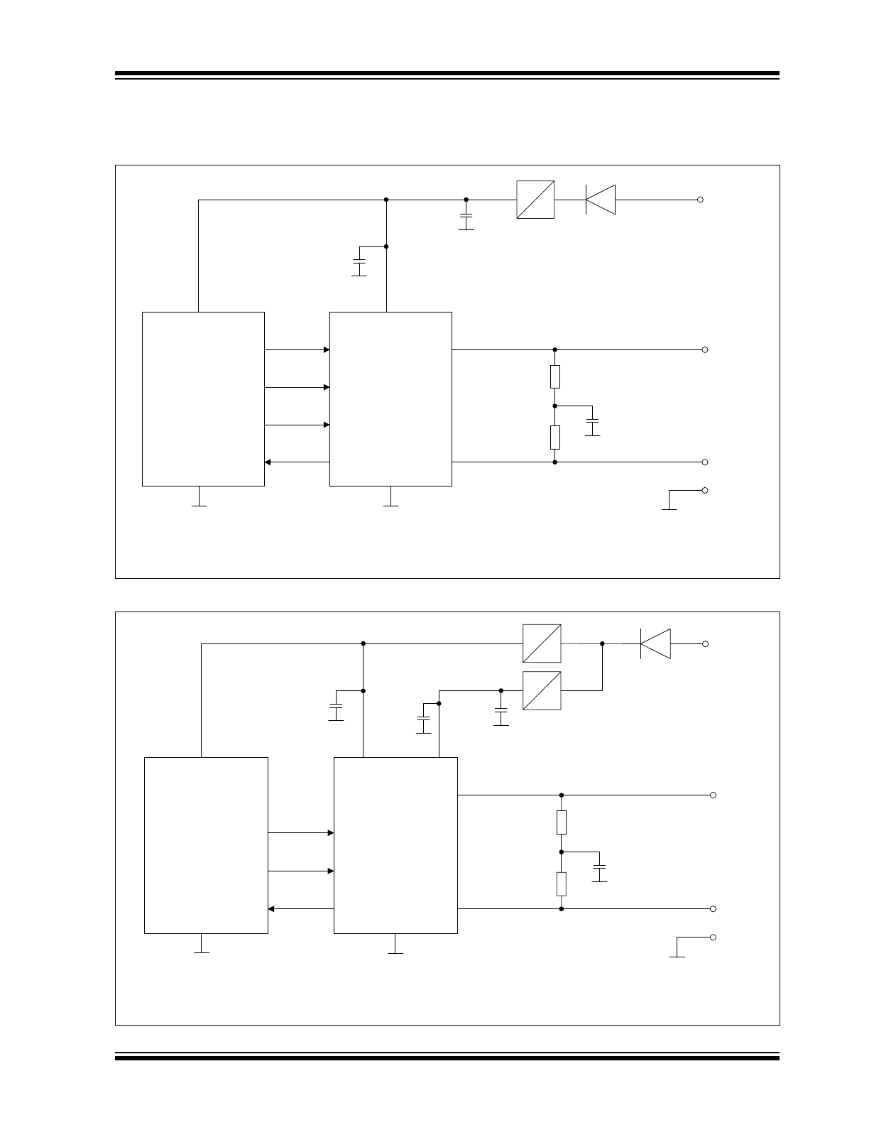
Functional Block Diagram
Notes:
1. Pin 5: ATA6563: VIO
ATA6562: NSIL (the VIO line and the VCC line are internally connected)
2. HSC: High-speed comparator
3. WUC: Wake-up comparator
Temperature
Protection
TXD
Time-Out-
Timer
Control Unit
MUX
Slope Control
and
Driver
Wake-up
Filter
CANH
CANL
TXD
GND
VCC
RXD
STBY
VIO
NSIL
VIO
(1)
VIO
(1)
VIO
(
VCC
HSC
(2)
WUC
(3)
VIO
(1)
1
8
4
2
6
7
3
5
(1)
5
(1)
ATA6562/3
DS20005790B-page 4
2017 Microchip Technology Inc.
1.0
FUNCTIONAL DESCRIPTION
The ATA6562/ATA6563 is a stand-alone dual
high-speed CAN transceiver compliant with the
ISO 11898-2, ISO 11898-2: 2016, ISO 11898-5 and
SAE J2962-2 CAN standards. It provides a very low
current consumption in Standby mode and wake-up
capability via the CAN bus. There are two versions
available, only differing in the function of pin 5:
• ATA6562: The pin 5 is the control input for Silent
mode NSIL, allowing the ATA6562 to only receive
data but not send data via the bus. The output
driver stage is disabled. The VIO line and the
VCC line are internally connected, this sets the
signal levels of the TXD, RXD, STBY, and NSIL
pins to levels compatible with 5V microcontrollers.
• ATA6563: The pin 5 is the VIO pin and should be
connected to the microcontroller supply voltage.
This allows direct interfacing to microcontrollers
with supply voltages down to 3V and adjusts the
signal levels of the TXD, RXD, and STBY pins to
the I/O levels of the microcontroller. The I/O ports
are supplied by the VIO pin.
1.1
Operating Modes
Each of the transceivers supports three operating
modes: Unpowered, Standby and Normal. The
ATA6562 additionally has the Silent mode. These
modes can be selected via the STBY and NSIL pin.
See
Figure 1-1
and
Table 1-1
for a description of the
operating modes.
FIGURE 1-1:
OPERATING MODES
1.1.1
NORMAL MODE
A low level on the STBY pin together with a high level
on pin TXD selects the Normal mode. In this mode the
transceiver is able to transmit and receive data via the
CANH and CANL bus lines (see
Functional Block
Diagram
). The output driver stage is active and drives
data from the TXD input to the CAN bus. The
high-speed comparator (HSC) converts the analog
Note
: For the ATA6563 NSIL is internally set to “1”.
Unpowered
Mode
Standby
Mode
V
CC
< V
uvd(VCC)
V
CC
< V
uvd(VCC)
Silent
Mode
V
CC
> V
uvd(VCC)
V
CC
< V
uvd(VCC)
STBY = 1
STBY = 0 and
(NSIL = 0 or
TXD
= 0)
Normal
Mode
STBY = 0 and
NSIL = 1 and
TXD
= 1 and
Error = 0
STBY = 1
NSIL = 1 and TXD
= 1 and Error = 0
NSIL = 0 or TXD
= 1
ATA6562
Unpowered
Mode
Standby
Mode
V
CC
< V
uvd(VCC)
or
V
IO
< V
uvd(VIO)
Silent
Mode *
STBY = 1
STBY = 0 and
TXD
= 0
Normal
Mode
STBY = 0 and
TXD
= 1 and
Error = 0
STBY = 1
TXD
= 1 and Error = 0
TXD
= 1
ATA6563
V
CC
< V
uvd(VCC)
or
V
IO
< V
uvd(VIO)
V
CC
< V
uvd(VCC)
or
V
IO
< V
uvd(VIO)
V
CC
> V
uvd(VCC)
or
V
IO
> V
uvd(VIO)
* Silent Mode is externally not accessible
TABLE 1-1:
OPERATING MODES
Mode
Inputs
Outputs
STBY
NSIL
PIN TXD
CAN Driver
Pin RXD
Unpowered
X
(
3
)
X
(
3
)
X
(
3
)
Recessive
Recessive
Standby
HIGH
X
(
3
)
X
(
3
)
Recessive
Active
(
4
)
Silent (only for ATA6562)
LOW
LOW
X
(
3
)
Recessive
Active
(
1
)
Normal
LOW
HIGH
(
2
)
LOW
Dominant
LOW
LOW
HIGH
(
2
)
HIGH
Recessive
HIGH
Note 1:
LOW if the CAN bus is dominant, HIGH if the CAN bus is recessive.
2:
Internally pulled up if not bonded out.
3:
Irrelevant
4:
Reflects the bus only for wake-up
2017 Microchip Technology Inc.
DS20005790B-page 5
ATA6562/3
data on the bus lines into digital data which is output to
pin RXD. The bus biasing is set to V
VCC
/2 and the
undervoltage monitoring of VCC is active.
The slope of the output signals on the bus lines is
controlled and optimized in a way that guarantees the
lowest possible electromagnetic emission (EME).
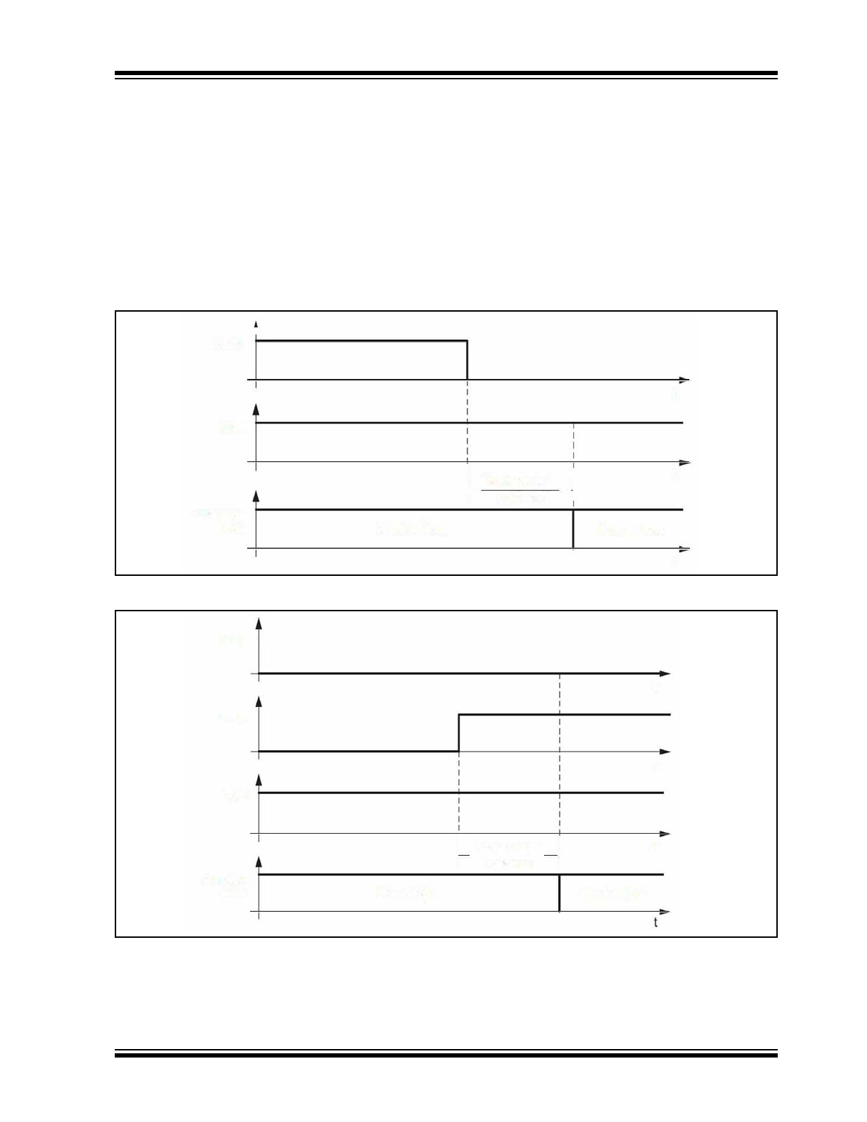
To switch the device in normal operating mode, set the
STBY pin to low and the TXD pin to high (see
Table 1-1
and
Figure 1-2
). The STBY pin provides a pull-up
resistor to VIO, thus ensuring a defined level if the pin
is open.
Please note that the device cannot enter Normal mode
as long as TXD is at ground level.
The switching into Normal mode is depicted in the
following two figures.
FIGURE 1-2:
SWITCHING FROM STANDBY MODE TO NORMAL MODE (NSIL = HIGH)
FIGURE 1-3:
SWITCHING FROM SILENT MODE TO NORMAL MODE
1.1.2
SILENT MODE (ONLY WITH THE
ATA6562)
A low level on the NSIL pin (available on pin 5) and on
the STBY pin selects Silent mode. This receive-only
mode can be used to test the connection of the bus
medium. In Silent mode the ATA6562 can still receive
data from the bus, but the transmitter is disabled and
therefore no data can be sent to the CAN bus. The bus
pins are released to recessive state. All other IC
/
#$)!/
!/
)-/ !/
/
)'*, "%//
/
.(/+/
!&/ !/
0
0
'(-%#0
%0
#-0%0
0
-+
$&)
0
0
0
/,0".0
0
%*"0 %0
ATA6562/3
DS20005790B-page 6
2017 Microchip Technology Inc.
functions, including the high-speed comparator (HSC),
continue to operate as they do in Normal mode. Silent
mode can be used to prevent a faulty CAN controller
from disrupting all network communications.
1.1.3
STANDBY MODE
A high level on the STBY pin selects Standby mode. In
this mode the transceiver is not able to transmit or cor-
rectly receive data via the bus lines. The transmitter
and the high-speed comparator (HSC) are switched off
to reduce current consumption.
For ATA6562 only: In the event the NSIL input pin is set
to low in Standby mode, the internal pull-up resistor
causes an additional quiescent current from VIO to
GND. Microchip recommends setting the NSIL pin to
high in Standby mode.
1.1.3.1
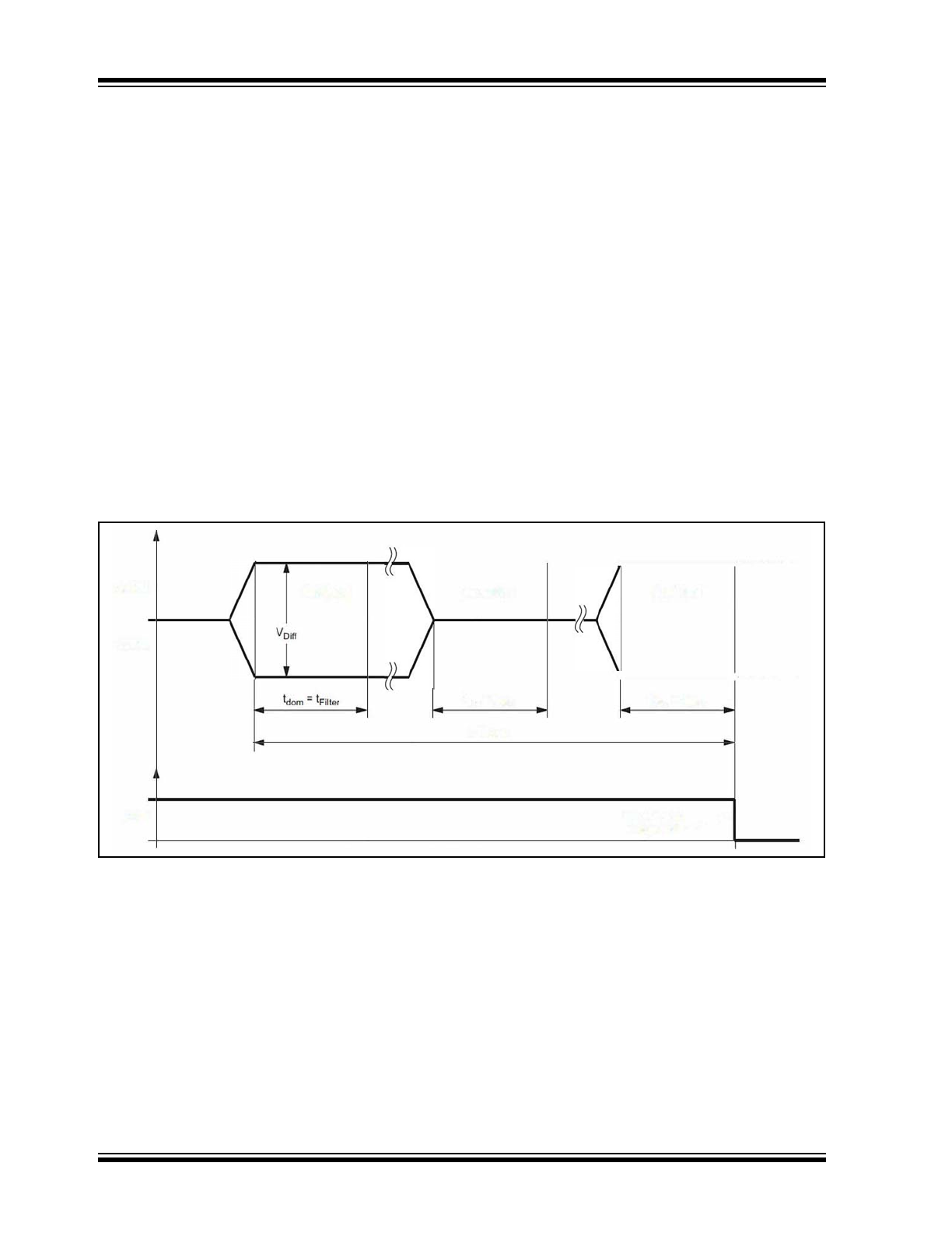
Remote Wake-up via the CAN Bus
In Standby mode the bus lines are biased to ground to
reduce current consumption to a minimum. The
ATA6562/ATA6563 monitors the bus lines for a valid
wake-up pattern as specified in the ISO 11898-2: 2016.
This filtering helps to avoid spurious wake-up events,
which would be triggered by scenarios such as a dom-
inant clamped bus or by a dominant phase due to
noise, spikes on the bus, automotive transients or EMI.
The wake-up pattern consists of at least two
consecutive dominant bus levels for a duration of at
least t
Filter
, each separated by a recessive bus level
with a duration of at least t
Filter
. Dominant or recessive
bus levels shorter than t
Filter
are always being ignored.
The complete dominant-recessive-dominant pattern as
shown in
Figure 1-4
, must be received within the bus
wake-up time-out time t
Wake
to be recognized as a valid
wake-up pattern. Otherwise, the internal wake-up logic
is reset and then the complete wake-up pattern must
be retransmitted to trigger a wake-up event. Pin RXD
remains at high level until a valid wake-up event has
been detected.
During Normal mode, at a VCC undervoltage condition
or when the complete wake-up pattern is not received
within t
Wake
, no wake-up is signalled at the RXD pin.
FIGURE 1-4:
TIMING OF THE BUS WAKE-UP PATTERN (WUP) IN STANDBY MODE
When a valid CAN wake-up pattern is detected on the
bus, the RXD pin switches to low to signal a wake-up
request. A transition to Normal mode is not triggered
until the STBY pin is forced back to low by the micro-
controller.
1.2
Fail-safe Features
1.2.1
TXD DOMINANT TIME-OUT
FUNCTION
A TXD dominant time-out timer is started when the
TXD pin is set to low. If the low state on the TXD pin
persists for longer than t
to(dom)TXD
, the transmitter is
disabled, releasing the bus lines to recessive state.
This function prevents a hardware and/or software
application failure from driving the bus lines to a perma-
nent dominant state (blocking all network communica-
tions). The TXD dominant time-out timer is reset when
the the TXD pin is set to high. If the low state on the
TXD pin was longer than t
to(dom)TXD
, then the TXD pin
has to be set to high longer 4 µs in order to reset the
TXD dominant time-out timer..
1.2.2
INTERNAL PULL-UP STRUCTURE
AT THE TXD AND STBY INPUT PINS
The TXD and STBY pins have an internal pull-up to
VIO. This ensures a safe, defined state in case one or
both pins are left floating. Pull-up currents flow in these
2017 Microchip Technology Inc.
DS20005790B-page 7
ATA6562/3
pins in all states, meaning all pins should be in high
state during Standby mode to minimize the current con-
sumption.
1.2.3
UNDERVOLTAGE DETECTION ON
PIN VCC
If V
VCC
or V
VIO
drops below its undervoltage detection
levels (V
uvd(VCC)
and V
uvd(VIO)
)(see
Section 2.0, Elec-
trical Characteristics
), the transceiver switches off and
disengages from the bus until V
VCC
and V
VIO
has
recovered. The low-power wake-up comparator is only
switched off during a VCC and VIO undervoltage. The
logic state of the STBY pin is ignored until the V
VCC
voltage or V
VIO
voltage has recovered.
1.2.4
BUS WAKE UP ONLY AT
DEDICATED WAKE-UP PATTERN
Due to the implementation of the wake-up filtering the
ATA6562/ATA6563 does not wake-up when the bus is
in a long dominant phase, it only wakes up at a dedi-
cated wake-up pattern as specified in the ISO
11898-2: 2016. This means for a valid wake-up at least
two consecutive dominant bus levels for a duration of
at least t
Filter
, each separated by a recessive bus level
with a duration of at least t
Filter
must be received via the
bus. Dominant or recessive bus levels shorter than t
Fil-
ter
are always being ignored. The complete domi-
nant-recessive-dominant pattern as shown in
Figure 1-4
, must be received within the bus wake-up
time-out time t
Wake
to be recognized as a valid wake-up
pattern. This filtering leads to a higher robustness
against EMI and transients and reduces therefore the
risk of an unwanted bus wake- up significantly.
1.2.5
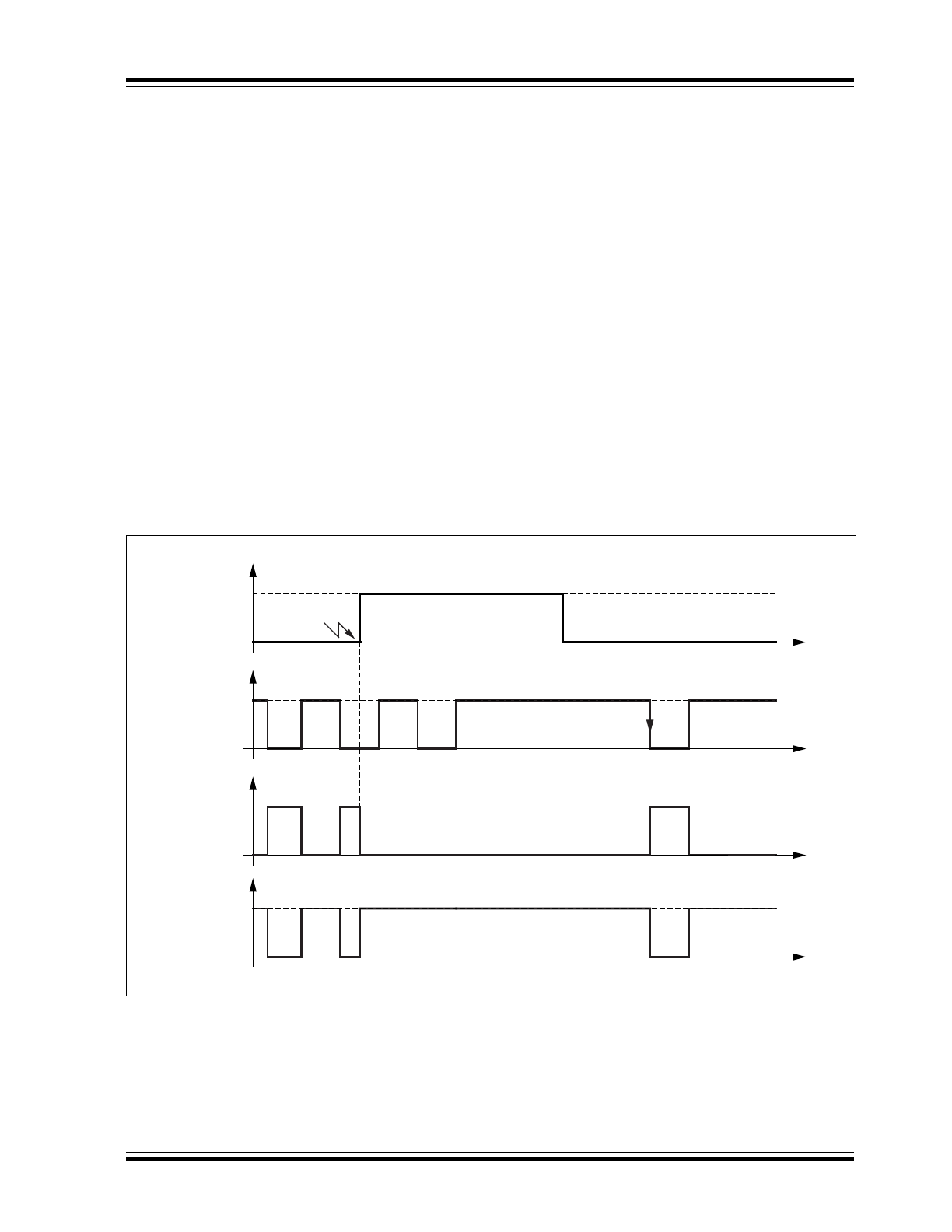
OVERTEMPERATURE
PROTECTION
The output drivers are protected against overtempera-
ture conditions. If the junction temperature exceeds the
shutdown junction temperature, T
Jsd
, the output drivers
are disabled until the junction temperature drops below
T
Jsd
and pin TXD is at high level again. The TXD con-
dition ensures that output driver oscillations due to tem-
perature drift are avoided.
FIGURE 1-5:
RELEASE OF TRANSMISSION AFTER OVERTEMPERATURE CONDITION
1.2.6
SHORT-CIRCUIT PROTECTION OF
THE BUS PINS
The CANH and CANL bus outputs are short-circuit pro-
tected, either against GND or a positive supply voltage.
A current-limiting circuit protects the transceiver
against damage. If the device is heating up due to a
continuous short on CANH or CANL, the internal over-
temperature protection switches the bus transmitter off.
Failure
Overtemp
GND
TXD
Overtemperature
R
D
R
t
t
t
OT
BUS V
DIFF
(CANH-CANL)
VIO
R
D
D
t
t
RXD
VIO
GND
ATA6562/3
DS20005790B-page 8
2017 Microchip Technology Inc.
1.2.7
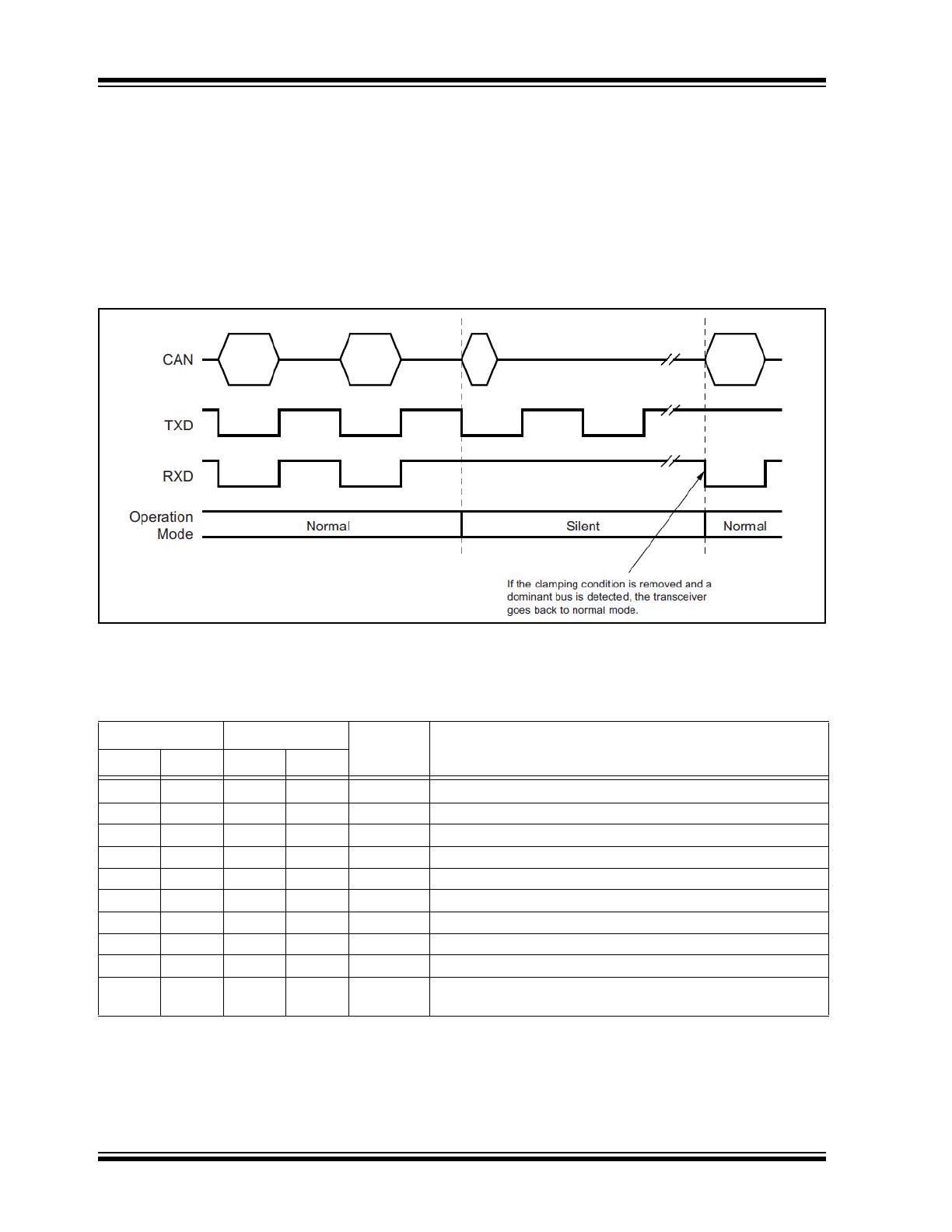
RXD RECESSIVE CLAMPING
This fail-safe feature prevents the controller from
sending data on the bus if its RXD is clamped to HIGH
(e.g., recessive). That is, if the RXD pin cannot
signalize a dominant bus condition because it is e.g,
shorted to VCC, the transmitter within
ATA6562/ATA6563 is disabled to avoid possible data
collisions on the bus. In Normal and Silent mode (only
ATA6562), the device permanently compares the state
of the high-speed comparator (HSC) with the state of
the RXD pin. If the HSC indicates a dominant bus state
for more than t
RC_det
without the RXD pin doing the
same, a recessive clamping situation is detected and
the transceiver is forced into Silent mode. This
Fail-safe mode is released by either entering Standby
or Unpowered mode or if the RXD pin is showing a
dominant (e.g., low) level again.
FIGURE 1-6:
RXD RECESSIVE CLAMPING DETECTION
1.3
Pin Description
The descriptions of the pins are listed in
Table 1-2
.
TABLE 1-2:
PIN FUNCTION TABLE
ATA6562
ATA6563
Pin Name
Description
SOIC8
VDFN8
SOIC8
VDFN8
1
1
1
1
TXD
Transmit data input
2
2
2
2
GND
Ground1 supply
3
3
3
3
VCC
Supply voltage
4
4
4
4
RXD
Receive data output; reads out data from the bus lines
—
—
5
5
VIO
Supply voltage for I/O level adapter
5
5
—
—
NSIL
Silent mode control input (low active);
6
6
6
6
CANL
Low-level CAN bus line
7
7
7
7
CANH
High-level CAN bus line
8
8
8
8
STBY
Standby mode control input
—
9
—
9
EP
Exposed Thermal Pad: Heat slug, internally connected to the
GND pin.
2017 Microchip Technology Inc.
DS20005790B-page 9
ATA6562/3
1.4
Typical Application
Typical Application ATA6562
Typical Application ATA6563
Note: For VDFN8 package: EP (heatslug) must always be connected to GND.
Microcontroller
ATA6562
VDD
GND
GND
1
2
3
4
NSIL
STBY
8
7
6
5
TXD
RXD
CANH
CANL
CANH
CANL
BAT
VCC
100 nF
22 µF
(1)
5V
12V
+
GND
(1) The size of this capacitor depends on the used external voltage regulator
Note: For VDFN8 package: EP (heatslug) must always be connected to GND.
Microcontroller
ATA6563
VDD
GND
GND
1
2
3
4
7
6
5
TXD
RXD
CANH
CANL
CANH
CANL
BAT
VCC
100 nF
22 µF
(1)
3.3V
12V
+
GND
(1) The size of this capacitor depends on the used external voltage regulator
STBY
8
VIO
100 nF
5V
12V
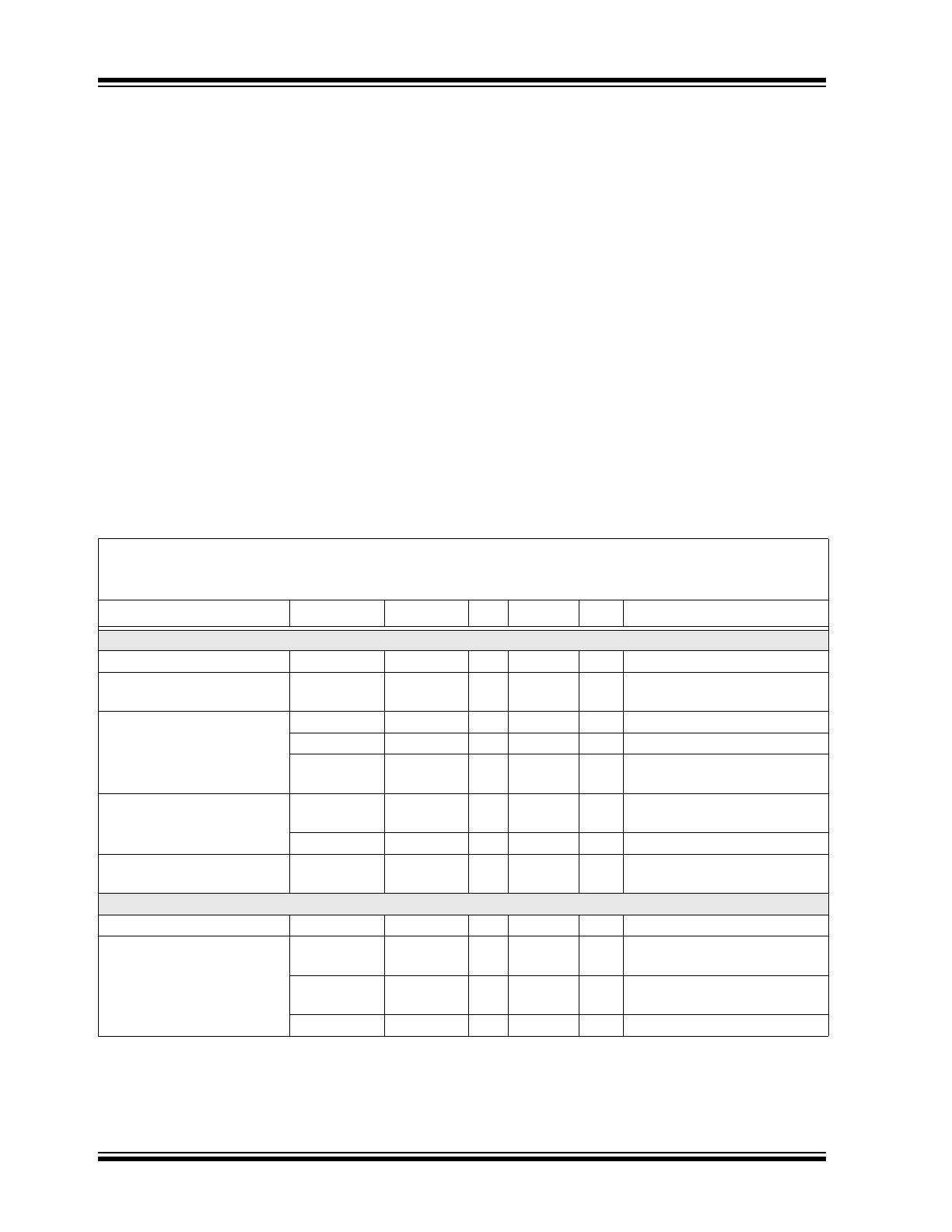
ATA6562/3
DS20005790B-page 10
2017 Microchip Technology Inc.
2.0
ELECTRICAL CHARACTERISTICS
Absolute Maximum Ratings
(†)
DC Voltage at CANH, CANL (V
CANH
, V
CANL
) ................................................................................................–27 to +42V
Transient Voltage at CANH, CANL (according to ISO 7637 part 2) (V
CANH
, V
CANL
) .................................–150 to +100V
Max. differential bus voltage (V
Diff
)...................................................................................................................–5 to +18V
DC voltage on all other pins (V
X
) .................................................................................................................–0.3 to +5.5V
ESD according to IBEE CAN EMC - Test specification following IEC 61000-4-2 — Pin CANH, CANL ..................±8 kV
ESD (HBM following STM5.1 with 1.5 kΩ/100 pF) - Pins CANH, CANL to GND.................................................... ±6 kV
Component Level ESD (HBM according to ANSI/ESD STM5.1, JESD22-A114, AEC-Q100 (002) ........................±4 kV
CDM ESD STM 5.3.1 ..............................................................................................................................................±750V
ESD machine model AEC-Q100-RevF(003) ...........................................................................................................±200V
Virtual Junction Temperature (T
vJ
) .............................................................................................................–40 to +175°C
Storage Temperature Range (T
stg
) .........................................................................................................-55°C to +150°C
† Notice:
Stresses above those listed under “Maximum Ratings” may cause permanent damage to the device. This is
a stress rating only and functional operation of the device at those or any other conditions above those indicated in the
operation listings of this specification is not implied. Exposure to maximum rating conditions for extended periods may
affect device reliability.
TABLE 2-1:
ELECTRICAL CHARACTERISTICS
Electrical Specifications:
The values below are valid for each of the two identical integrated CAN transceivers.
Grade 1: T
amb
= -40°C to +125°C and Grade 0: T
amb
= -40°C to +150°C; V
VCC
= 4.5V to 5.5V; R
L
= 60Ω, C
L
= 100 pF
unless specified otherwise; all voltages are defined in relation to ground; positive currents flow into the IC.
Parameters
Sym.
Min.
Typ.
Max.
Units
Conditions
Supply, Pin VCC
Supply Voltage
V
VCC
4.5
—
5.5
V
Supply Current in Silent
Mode
I
VCC_sil
1.9
2.5
3.0
mA
Silent mode, V
TXD
= V
VIO
Supply Current in Normal
Mode
I
VCC_rec
2
—
5
mA
recessive, V
TXD
= V
VIO
I
VCC_dom
30
50
70
mA
dominant, V
TXD
= 0V
I
VCC_short
—
—
85
mA
short between CANH and
CANL(
Note 1
)
Supply Current in Standby
Mode
I
VCC_STBY
—
—
12
µA
VCC = VIO,
V
TXD
= V
NSIL
= V
VIO
I
VCC_STBY
—
7
—
µA
T
a
= 25°C (
Note 3
)
Undervoltage Detection
Threshold on Pin VCC
V
uvd(VCC)
2.75
—
4.5
V
I/O Level Adapter Supply, Pin VIO (only with the ATA6563)
Supply voltage on pin VIO
V
VIO
2.8
—
5.5
V
Supply current on pin VIO
I
VIO_rec
10
80
250
µA
Normal and Silent mode
recessive, V
TXD
= V
VIO
I
VIO_dom
50
350
500
µA
Normal and Silent mode
dominant, V
TXD
= 0V
I
VIO_STBY
—
—
1
µA
Standby mode
Note 1:
100% correlation tested
2:
Characterized on samples
3:
Design parameter