
2016 Microchip Technology Inc.
DS20005597A-page 1
AT9933
Features
• Constant Current LED Driver
• Steps Input Voltage Up or Down
• Low Electromagnetic Interference (EMI)
• Variable Frequency Operation
• Internal 75V Linear Regulator
• Input and Output Current Sensing
• Input Current Limit
• Enable and Pulse-width Modulation (PWM)
Dimming
• Ambient Temperature Rating of up to 125°C
Applications
• LED Lighting Applications
General Description
The AT9933 is a variable frequency PWM controller IC,
designed to control an LED lamp driver using a
low-noise boost-buck (Ćuk) topology. It uses
patent-pending Hysteretic Current-mode control to
regulate both the input and the output currents. This
enables superior input surge immunity without the
necessity for complex loop compensation. Input
current control enables current limiting during Startup,
Input Undervoltage and Output Overload conditions.
The AT9933 provides a low-frequency PWM dimming
input that can accept an external control signal with a
duty cycle of 0%–100% and a high dimming ratio.
This AT9933-based LED driver is ideal for LED lamps.
The part is rated for up to 125°C ambient temperatures.
Package Type
REF
CS2
VDD
PWMD
VIN
CS1
GND
GATE
8
7
6
5
1
2
3
4
8-lead SOIC
(Top View)
See
Table 2-1
for pin information.
Hysteretic Boost-Buck (Ćuk) LED Driver IC
AT9933
DS20005597A-page 2
2016 Microchip Technology Inc.
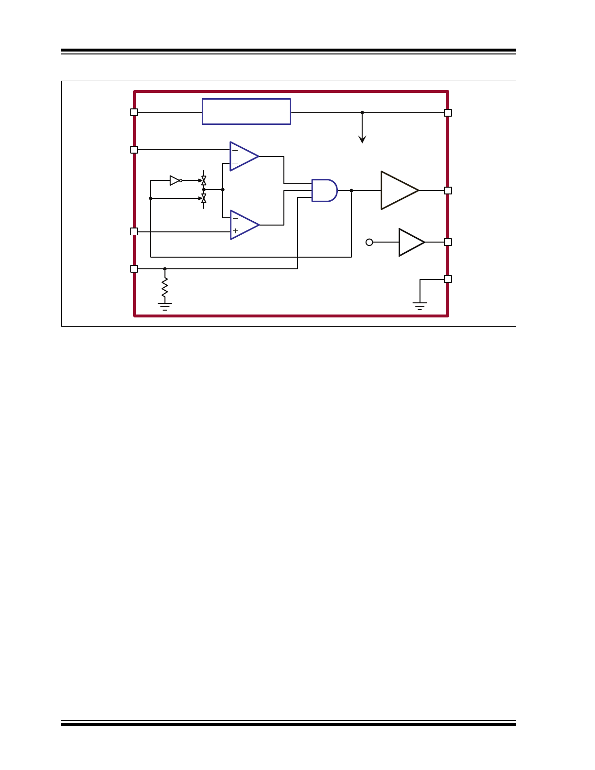
Functional Block Diagram
Regulator
7.5V
VIN
CS1
CS2
PWMD
GATE
VDD
REF
GND
1.25V
AT9933
Input Comparator
Output Comparator
0mV
100mV
2016 Microchip Technology Inc.
DS20005597A-page 3
AT9933
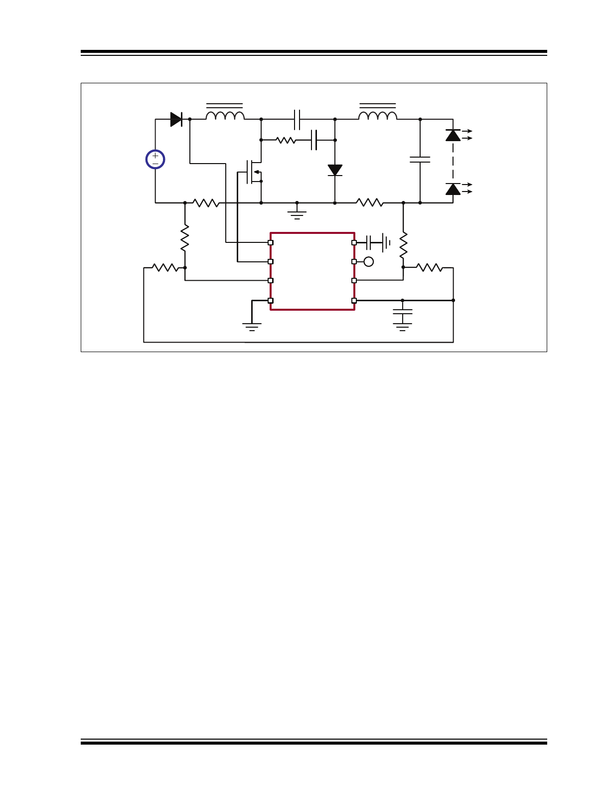
Typical Application
VIN
GATE
CS1
GND
VDD
PWMD
CS2
REF
VDC
L
1
L
2
C
1
Q
1
D
1
R
CS1
R
S2
R
REF2
R
REF1
R
S1
C
2
D
2
(optional)
-
VO
+
C
3
R
CS2
D
3
R
D
C
D
AT9933
Circuit
AT9933
DS20005597A-page 4
2016 Microchip Technology Inc.
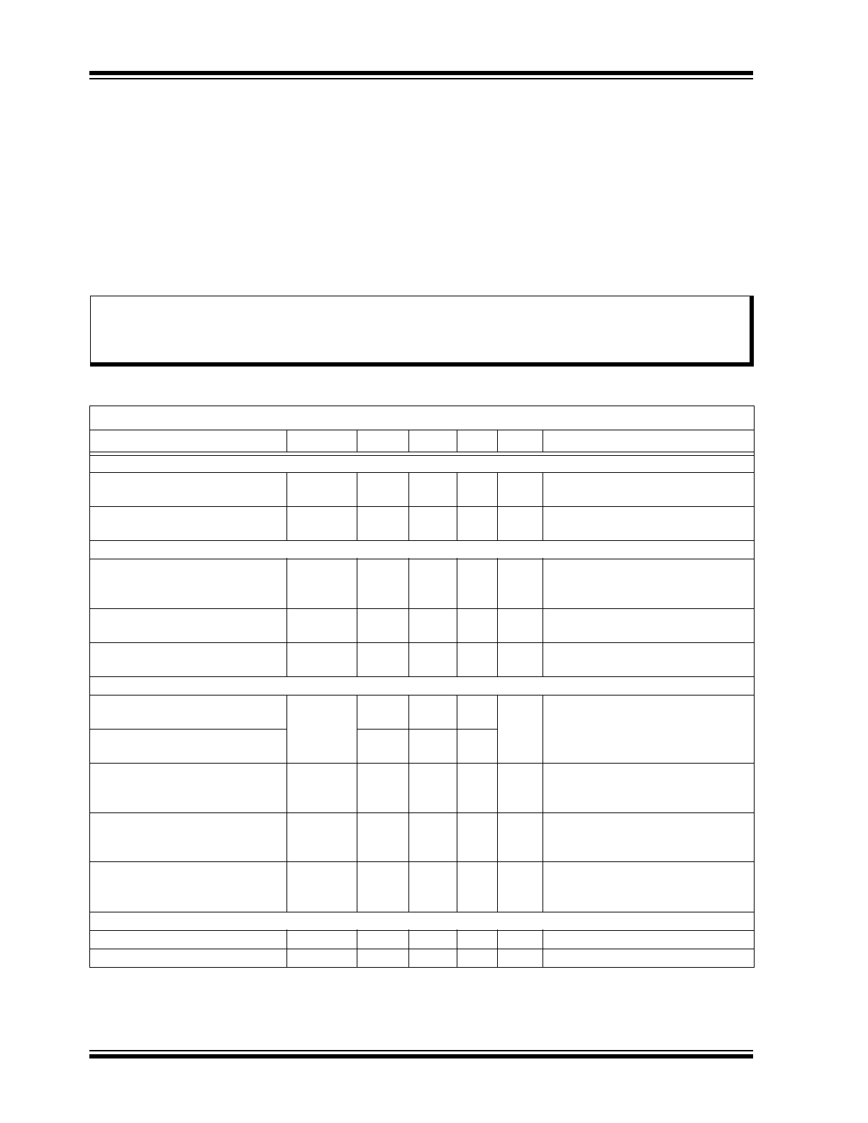
1.0
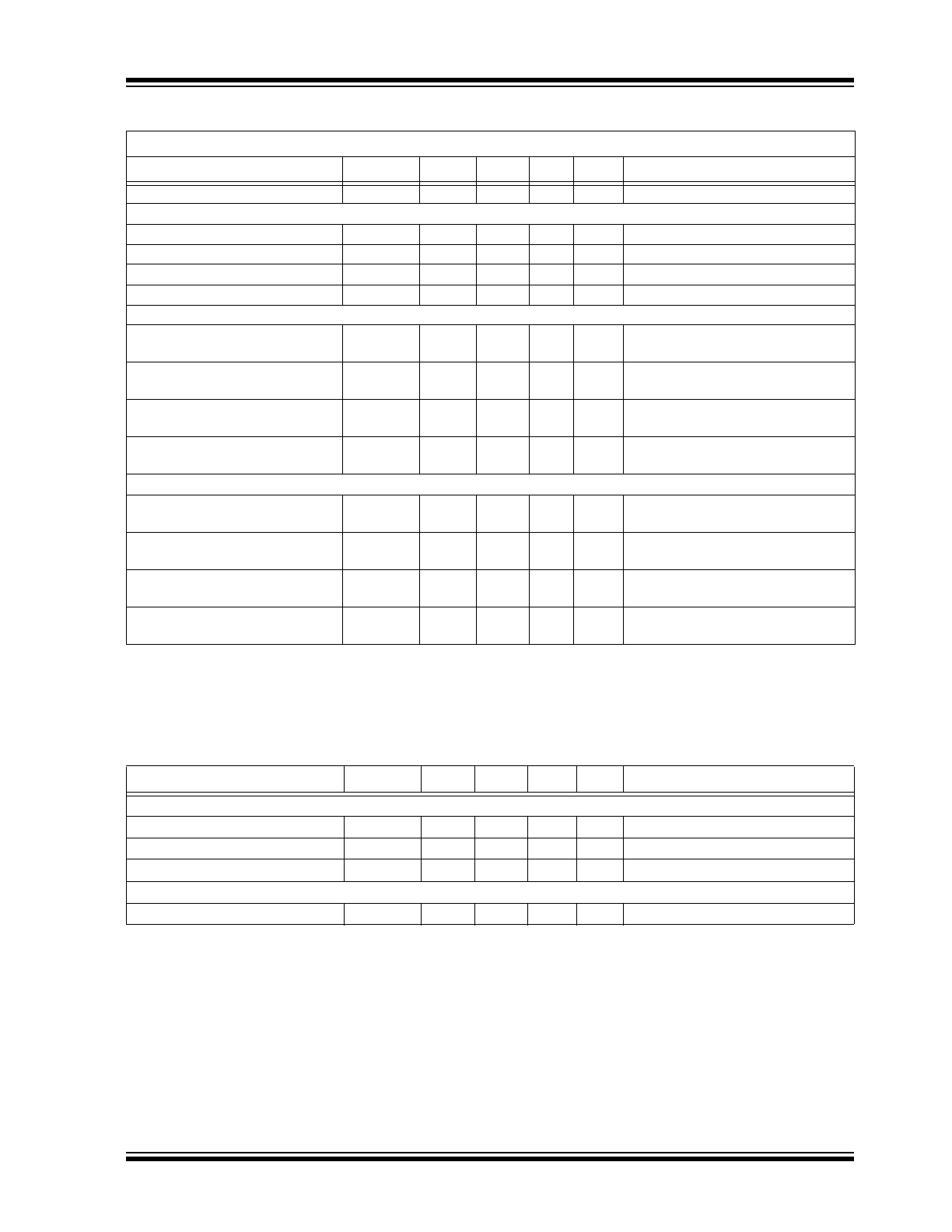
ELECTRICAL CHARACTERISTICS
Absolute Maximum Ratings†
V
IN
to GND ................................................................................................................................................–0.5V to +75V
CS1, CS2, PWMD and GATE to GND ............................................................................................. –0.3V to V
DD
+0.3V
V
DD(MAX)
................................................................................................................................................................. +12V
Operating Temperature Range............................................................................................................. –40°C to +125°C
Junction Temperature.......................................................................................................................................... +150°C
Storage Temperature Range ............................................................................................................... –65°C to +150°C
Continuous Power Dissipation (T
A
= +25°C):
8-lead SOIC ............................................................................................................................................ 700 mW
† Notice: Stresses above those listed under “Absolute Maximum Ratings” may cause permanent damage to the
device. This is a stress rating only, and functional operation of the device at those or any other conditions above those
indicated in the operational sections of this specification is not intended. Exposure to maximum rating conditions for
extended periods may affect device reliability.
ELECTRICAL CHARACTERISTICS
Electrical Specifications: Specifications are at T
A
= 25°C, V
IN
= Open and V
DD
= 7.5V unless otherwise noted.
Parameter
Sym.
Min.
Typ.
Max.
Unit
Conditions
INPUT
Input DC Supply Voltage Range
V
INDC
Note 3
—
75
V
DC input voltage
(
Note 1
and
Note 2
)
Shutdown Mode Supply Current
I
INSD
—
0.5
1
mA
PWMD connected to GND,
V
IN
= 12V (
Note 2
)
INTERNAL REGULATOR
Internally Regulated Voltage
V
DD
7
7.5
9
V
V
IN
= 8V–75V, I
DD(EXT)
= 0,
500 pF capacitor at GATE,
PWMD = GND (
Note 1
)
V
DD
Undervoltage Lockout
Threshold
UVLO
6.35
6.7
7.05
V
V
DD
rising (
Note 1
)
V
DD
Undervoltage Lock-out
Hysteresis
∆UVLO
—
500
—
mV
REFERENCE
REF Pin Voltage
0°C < T
A
< +85°C
V
REF
1.212
1.25
1.288
V
REF bypassed with a 0.1 µF
capacitor to GND, I
REF
= 0,
PWMD = 5V
REF Pin Voltage
–40°C < T
A
< +125°C
1.187
1.25
1.312
Line Regulation of Reference
Voltage
V
REFLINE
0
—
20
mV
REF bypassed with a 0.1 µF capac-
itor to GND, I
REF
= 0,
V
DD
= 7V–9V, PWMD = 5V
Reference Output Current Range
I
REF
–0.01
—
500
µA
REF bypassed with a 0.1 µF capac-
itor to GND, I
REF
= 0, V
DD
= 7V–9V,
PWMD = 5V
Load Regulation of Reference
Voltage
V
REFLOAD
0
—
10
mV
REF bypassed with a 0.1 µF capac-
itor to GND, I
REF
= 0 µA–500 µA,
PWMD = 5V
PWM DIMMING
PWMD Input Low Voltage
V
PWMD(LO)
—
—
0.8
V
V
DD
= 7V–9V (
Note 1
)
PWMD Input High Voltage
V
PWMD(HI)
2
—
—
V
V
DD
= 7V–9V (
Note 1
)
Note 1:
Specifications apply over the full operating ambient temperature range of –40ºC < T
A
< +125ºC.
2: Also limited by package power dissipation limit, whichever is lower
3: Depends on the current drawn by the part. See
Section 4.0 “Application Information”
2016 Microchip Technology Inc.
DS20005597A-page 5
AT9933
PWMD Pull-down Resistance
R
PWMD
50
100
150
kΩ
V
PWMD
= 5V
GATE DRIVER
GATE Short Circuit Current
I
SOURCE
0.165
—
—
A
V
GATE
= 0V
GATE Sinking Current
I
SINK
0.165
—
—
A
V
GATE
= V
DD
GATE Output Rise Time
T
RISE
—
30
50
ns
C
GATE
= 500 pF
GATE Output Fall Time
T
FALL
—
30
50
ns
C
GATE
= 500 pF
INPUT CURRENT SENSE COMPARATOR
Voltage required to turn on GATE V
TURNON1
85
100
115
mV
C
S2
= 200 mV, C
S1
increasing,
GATE goes LOW to HIGH (
Note 1
)
Voltage required to turn off GATE
V
TURN-
OFF1
–15
0
15
mV
C
S2
= 200 mV, C
S1
decreasing,
GATE goes HIGH to LOW (
Note 1
)
Delay to Output (Turn-on)
T
D1,ON
—
150
250
ns
C
S2
= 200 mV,
C
S1
= 50 mV to +200 mV step
Delay to Output (Turn-off)
T
D1,OFF
—
150
250
ns
C
S2
= 200 mV,
C
S1
= 50 mV to –100 mV step
OUTPUT CURRENT SENSE COMPARATOR
Voltage required to turn on GATE V
TURNON2
85
100
115
mV
C
S1
= 200 mV, C
S2
increasing,
GATE goes LOW to HIGH (
Note 1
)
Voltage required to turn off GATE
V
TURN-
OFF2
–15
0
15
mV
C
S1
= 200 mV, C
S2
decreasing,
GATE goes HIGH to LOW (
Note 1
)
Delay to Output (Turn-on)
T
D2,ON
—
150
250
ns
C
S1
= 200 mV,
C
S2
= 50 mV to +200 mV step
Delay to Output (Turn-off)
T
D2,OFF
—
150
250
ns
C
S1
= 200 mV,
C
S2
= 50 mV to –100 mV step
TEMPERATURE SPECIFICATIONS
Parameter
Sym.
Min.
Typ.
Max.
Unit
Conditions
TEMPERATURE RANGE
Operating Temperature
T
A
–40
—
+125
°C
Junction Temperature
T
J
—
—
+150
°C
Storage Temperature
T
S
–65
—
+150
°C
PACKAGE THERMAL RESISTANCE
8-lead SOIC
JA
—
+101
—
°C/W
Note 1
Note 1: Mounted on a FR-4 board, 25 mm x 25 mm x 1.57 mm
ELECTRICAL CHARACTERISTICS (CONTINUED)
Electrical Specifications: Specifications are at T
A
= 25°C, V
IN
= Open and V
DD
= 7.5V unless otherwise noted.
Parameter
Sym.
Min.
Typ.
Max.
Unit
Conditions
Note 1:
Specifications apply over the full operating ambient temperature range of –40ºC < T
A
< +125ºC.
2: Also limited by package power dissipation limit, whichever is lower
3: Depends on the current drawn by the part. See
Section 4.0 “Application Information”

AT9933
DS20005597A-page 6
2016 Microchip Technology Inc.
2.0
PIN DESCRIPTION
The details on the pins of AT9933 are listed on
Table 2-1
. Refer to
Package Type
for the location of
the pins.
TABLE 2-1:
PIN FUNCTION TABLE
Pin Number
Pin Name
Description
1
VIN
This pin is the input of an 8V–75V voltage regulator.
2
CS1
This pin is used to sense the input and output currents of the boost-buck converter. It is
a non-inverting input of the internal comparator.
3
GND
This is the ground return for all the internal circuitry. This pin must be electrically
connected to the ground of the power train.
4
GATE
This pin is the output gate driver for an external N-channel power Metal-oxide
Semiconductor Field-effect Transistor (MOSFET).
5
PWMD
When this pin is left open or pulled to GND, the gate driver is disabled. Pulling the pin to
a voltage greater than 2V will enable the gate driver output.
6
VDD
This is a power supply pin for all internal circuits. It must be bypassed to GND with a
low-ESR capacitor greater than 0.1 µF.
7
CS2
This pin is used to sense the input and output currents of the boost-buck converter. It is
a non-inverting input of the internal comparator.
8
REF
This pin provides accurate reference voltage. It must be bypassed with a
0.01 µF–0.1 µF capacitor to GND.
2016 Microchip Technology Inc.
DS20005597A-page 7
AT9933
3.0
DETAILED DESCRIPTION
3.1
Power Topology
The AT9933 is optimized to drive a Continuous
Conduction Mode (CCM) boost-buck DC/DC converter
topology commonly referred to as Ćuk converter.
(Refer to
Typical Application Circuit
.) This power
converter topology offers numerous advantages useful
for driving high-brightness light-emitting diodes (HB
LED). These advantages include step-up or step-down
voltage conversion ratio and low input and output
current ripple. The output load is decoupled from the
input voltage with a capacitor, making the driver
inherently failure-safe for the output load.
The AT9933 offers a simple and effective control
technique for a boost-buck LED driver. It uses two
Hysteretic mode controllers—one for the input and one
for the output. The outputs of these two hysteretic
comparators are ANDED and used to drive the external
FET. This control scheme gives accurate current
control and constant output current in the presence of
input voltage transients without the need for
complicated loop design.
3.2
Input Voltage Regulator
The AT9933 can be powered directly from its V
IN
pin
that can withstand a maximum voltage of up to 75V.
When a voltage is applied to the V
IN
pin, the AT9933
seeks to regulate a constant 7.5V (typical) at the V
DD
pin. The regulator also has a built-in undervoltage
lockout which shuts off the IC when the voltage at the
V
DD
pin falls below the UVLO threshold.
The V
DD
pin must be bypassed by a low-ESR capacitor
(≥0.1 μF) to provide a low-impedance path for the high
frequency current of the output gate driver.
The input current drawn from the V
IN
pin is the sum of
the 1 mA current drawn by the internal circuit and the
current drawn by the gate driver, which in turn depends
on the switching frequency and the gate charge of the
external FET. Refer to
Equation 3-1
.
EQUATION 3-1:
I
IN
1mA Q
G
f
S
+
=
In the above equation, f
S
is the switching frequency,
and Q
G
is the gate charge of the external FET which
can be obtained from the data sheet of the FET.
3.3
Minimum Input Voltage at V
IN
Pin
The minimum input voltage at which the converter will
start and stop depends on the minimum voltage drop
required for the linear regulator. The internal linear
regulator will control the voltage at the V
DD
pin when
V
IN
is between 8V and 75V. However, when the V
IN
is
less than 8V, the converter will still function as long as
the V
DD
is greater than the undervoltage lockout. Thus,
under certain conditions, the converter will be able to
start at V
IN
voltages of less than 8V. The start/stop
voltages at the V
IN
pin can be determined using the
maximum voltage drop across the linear regulator as a
function of the current drawn. The data for ambient
temperatures 25ºC and 125ºC are shown in
Figure 3-1
below:
3.5
3.0
2.5
2.0
1.5
1.0
0.5
0
0 1 2 3 4 5 6 7
I
IN
(mA)
Voltage Drop
(V
)
125
O
C
25
O
C
FIGURE 3-1:
Maximum Voltage Drop vs.
Input Current.
Assume an ambient temperature of 125°C. Provided
that the IC is driving a 15 nC gate charge FET at
300 kHz, the total input current is estimated to be
5.5 mA (using
Equation 3-1
). At this input current, the
maximum voltage drop from
Figure 3-1
can be
approximately estimated to be V
DROP
= 2.7V. However,
before the IC starts switching, the current drawn will be
1 mA. At this current level, the voltage drop is
approximately V
DROP1
= 0.5V. Thus, the start/stop V
IN
voltages can be computed as shown in
Equation 3-2
and
Equation 3-3
:
EQUATION 3-2:
V
IN START
–
UVLO
MAX
V
DROP1
+
=
6.95V 0.5V
+
=
7.45V
=
EQUATION 3-3:
V
IN STOP
–
UVLO
MAX
UVLO V
DROP
+
–
=
6.95V 0.5V
–
2.7V
+
=
9.15V
=
Note:
Since the gate driver draws too much cur-
rent in this situation, V
IN-START
is less than
V
IN-STOP
. The control IC will oscillate
between on and off if the input voltage is
between the start and stop voltages. In
these circumstances, it is recommended
that the input voltage be kept higher than
V
IN-STOP
. The IC will operate normally if
the input voltage is kept higher than 9.2V.

AT9933
DS20005597A-page 8
2016 Microchip Technology Inc.
In case of input transients that reduce the input voltage
below 8V (e.g. Cold Crank condition in an automotive
system), the V
IN
pin of the AT9933 can be connected to
the MOSFET drain through a switching diode using a
small (1 nF) capacitor between V
IN
and GND as long as
the drain voltage does not exceed 75V. Since the drain
of the FET is at a voltage equal to the sum of the input
and output voltages, the IC will still be operational when
the input goes below 8V. Therefore, a larger capacitor
is needed at the V
DD
pin to supply power to the IC when
the MOSFET is switched on.
In this case, V
DD UVLO
cannot be relied upon to turn off
the IC at low input voltages when input current levels
can get too large. In such cases, the input current limit
must be chosen to ensure that the input current is set
to a safe level.
3.4
Reference
An internally trimmed voltage reference of 1.25V is
provided at the REF pin. The reference can supply a
maximum output current of 500 µA to drive external
resistor dividers.
This reference can be used to set the current
thresholds of the two comparators as shown in the
Typical Application Circuit
section.
3.5
Current Comparators
The AT9933 features two identical comparators with a
built-in 100 mV hysteresis. When the GATE is low, the
inverting terminal is connected to 100 mV, but when the
GATE is high, it is connected to GND. One comparator
is used for the input current control and the other for the
output current control.
The input side hysteretic controller is in operation
during Start-up, Overload and Input Undervoltage
conditions. This ensures that the input current never
exceeds the designed value. During normal operation,
the input current is less than the programmed current.
Therefore, the output of the input side comparator will
be high. The output of the AND gate will then be
dictated by the output current controller.
The output side hysteretic comparator controls the
external MOSFET during Steady state operation of the
circuit. This comparator turns the MOSFET on and off
based on the LED current.
3.6
PWM Dimming
PWM Dimming can be achieved by applying a
TTL-compatible square wave signal to the PWM pin.
When the PWMD pin is pulled high, the gate driver is
enabled and the circuit operates normally. When the
PWMD pin is left open or connected to GND, the gate
driver is disabled and the external MOSFET turns off.
The signal at the PWMD pin inhibits the driver only and
the IC need not go through the entire start-up cycle
each time, ensuring a quick response time for the
output current. The recommended PWM dimming
frequency range is from 100 Hz to a few kilohertz.
The flying capacitor in the Ćuk converter (C1) is initially
charged to the input voltage VDC (through diodes D
1
and D
2
). When the circuit is turned on and reaches
Steady state, the voltage across C1 will be VDC+VO. In
the absence of diode D
2
, when the circuit is turned off,
capacitor C
1
will discharge through the LEDs and the
input voltage source VDC. Thus, during PWM dimming,
if capacitor C
1
has to be charged and discharged each
cycle, the transient response of the circuit will be
limited. By adding diode D
2
, the voltage across
capacitor C
1
is held at VDC+VO even when the circuit
is turned off, enabling the circuit to return quickly to its
Steady state (and bypassing the start-up stage) upon
being enabled.
2016 Microchip Technology Inc.
DS20005597A-page 9
AT9933
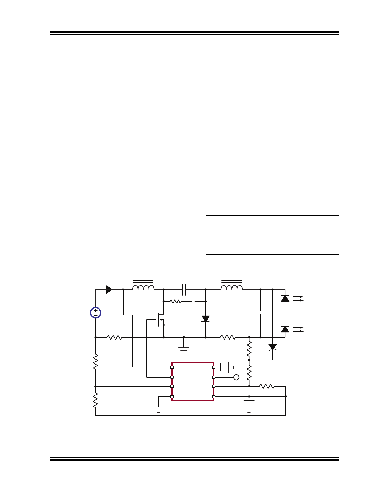
4.0
APPLICATION INFORMATION
4.1
Overvoltage Protection
Overvoltage protection can be added by splitting the
output side resistor R
S2
into two components and
adding a Zener diode D
3
. (Refer to
Figure 4-1
below.)
When there is an Open LED condition, the diode D
3
will
clamp the output voltage and the Zener diode current
will be regulated by the sum of R
S2A
and R
CS2
.
4.2
Damping Circuit
The Ćuk converter is inherently unstable when the
output current is being controlled. An uncontrolled input
current will lead to an undamped oscillation between L
1
and C
1
, causing excessively high voltages across
capacitor C
1
. To prevent these oscillations, a damping
circuit consisting of R
D
and C
D
is applied across the
capacitor C
1
. This damping circuit will stabilize the
circuit and help in the proper operation of the converter.
4.3
Design and Operation of the
Boost-buck Converter
For details on the design for a boost-buck converter
using the AT9933 and the calculation of the damping
components, refer to Application Notes AN-H51 and
AN-H58.
4.4
Design Example
The choice of the resistor dividers to set the input and
output current levels is illustrated by means of the
design example given below.
The parameters of the power circuit are:
V
IN MIN
9.01V
=
V
IN MAX
16V
=
V
O
28V
=
I
O
0.35A
=
f
S MIN
300kHz
=
Using these parameters, the values of the power stage
inductors and capacitor can be computed. (See figures
below.) Refer to Application Note AN-H51 for more
details.
L
1
82
H
=
L
2
150
H
=
C
1
0.22
F
=
The input and output currents for this design are:
I
IN MAX
1.6A
=
I
IN
0.21A
=
I
O
350mA
=
I
O
87.5mA
=
VIN
GATE
CS1
GND
VDD
PWMD
CS2
REF
VDC
L
1
L
2
C
1
Q
1
D1
R
CS1
R
S2A
R
REF2
R
REF1
R
S1
C
2
D
2
(optional)
-
VO
+
C
3
R
CS2
C
O
R
D
C
D
AT9933
R
S2B
D
3
FIGURE 4-1:
Design Example Circuit.

AT9933
DS20005597A-page 10
2016 Microchip Technology Inc.
4.5
Current Limits
The current sense resistor R
CS2
, combined with the
other resistors R
S2
and R
REF2
, determines the output
current limits.
The resistors can be chosen using
Equation 4-1
and
Equation 4-2
.
EQUATION 4-1:
I R
CS
1.2V
R
S
R
REF
-------------
0.05V
–
=
Where I is the current (either I
O
or I
IN
) and ∆I is the
peak-to-peak ripple in the current (either
∆I
O
or
∆I
IN
).
EQUATION 4-2:
I R
CS
0.1V
R
S
R
REF
-------------
0.1V
+
=
Where I is the current (either I
O
or I
IN
) and ∆I is the
peak-to-peak ripple in the current (either
∆I
O
or
∆I
IN
).
For the input side, the current level used in the
equations should be larger than the maximum input
current, so that it does not interfere with the normal
operation of the circuit. The peak input current can be
computed as shown in
Equation 4-3
.
EQUATION 4-3:
I
IN PK
I
IN MAX
I
IN
2
----------
+
=
1.706A
=
Assuming a 30% peak-to-peak ripple when the
converter is in Input Current Limit mode, the minimum
value of the input current is calculated as seen in
Equation 4-4
.
EQUATION 4-4:
I
LIM MIN
0.85 I
IN LIM
=
Setting
I
LIM MIN
1.05 I
IN PK
=
The current level to limit the converter can then be
computed. See equation
Equation 4-5
.
EQUATION 4-5:
I
IN LIM
1.05
0.85
----------
I
IN PK
=
2.1A
=
Using I
O
= 350 mA and ∆I
O
= 87.5 mA in
Equation 4-1
and
Equation 4-2
, R
CS2
= 1.78Ω and
R
S2
/R
REF2
= 0.5625.
Before the design of the output side is complete,
overvoltage protection has to be included in the design.
For this application, choose a 33V Zener diode. This is
the voltage at which the output will clamp in case of an
Open LED condition. For a 350 mW diode, the
maximum current rating at 33V works out to about
10 mA. Using a 2.5 mA current level during Open LED
conditions, and assuming the same R
S2
/R
REF2
ratio,
the Zener current limiting resistor can be determined as
illustrated in
Equation 4-6
.
EQUATION 4-6:
R
CS
R
S2A
+
120
=
Choose the following values for the resistors:
R
CS2
= 1.65Ω, 1/4W, 1%
R
REF2
= 10 kΩ, 1/8W, 1%
R
S2A
= 100Ω, 1/8W, 1%
R
S2B
= 5.23 kΩ, 1/8W, 1%
The current sense resistor needs to be at least a 1/4W,
1% resistor.
Similarly, using I
IN
= 2.1A and ∆I
IN
= 0.3 x I
IN
= 0.63 in
Equation 4-1
and
Equation 4-2
, the following values
can be determined:
R
S1
R
REF1
---------------
0.442
=
P
RCS1
I
2
IN LIM
R
CS1
=
Choose the following values for the resistors:
R
CS1
= parallel combination of three 0.68Ω, 1/2W, 5%
resistors
R
REF1
= 10kΩ, 1/8W, 1%
R
S1
= 4.42kΩ, 1/8W, 1%
R
CS1
0.228
=
1W
=