
2016 Microchip Technology Inc.
DS20005595A-page 1
AT9919
Features
• Hysteretic Control with High-side Current Sensing
• Wide Input Voltage Range: 4.5V to 40V
• >90% Efficiency
• Typical ±5% LED Current Accuracy
• Up to 2 MHz Switching Frequency
• Adjustable Constant LED Current
• Analog or Pulse-With Modulation (PWM) Control
Signal for PWM Dimming
• Overtemperature Protection
• –40ºC to +125ºC Operating Temperature Range
Applications
• LED Lighting Applications
General Description
The AT9919 is a PWM controller IC designed to drive
high-brightness LEDs using a buck topology. It
operates from an input voltage of 4.5 VDC to 40 VDC
and employs hysteretic control with a high-side current
sense resistor to set the constant output current.
The operating frequency range can be set by selecting
the proper inductor. Operation at high switching
frequency is possible since the hysteretic control
maintains accuracy even at high frequencies. This
permits the use of small inductors and capacitors,
minimizing space and cost in the overall system.
LED brightness control is achieved with PWM dimming
from an analog or PWM input signal. Unique PWM
circuitry allows true constant color with a high dimming
range. The dimming frequency is programmed using a
single external capacitor.
The AT9919 comes in a small, 8-lead DFN package
and is qualified for LED lighting applications.
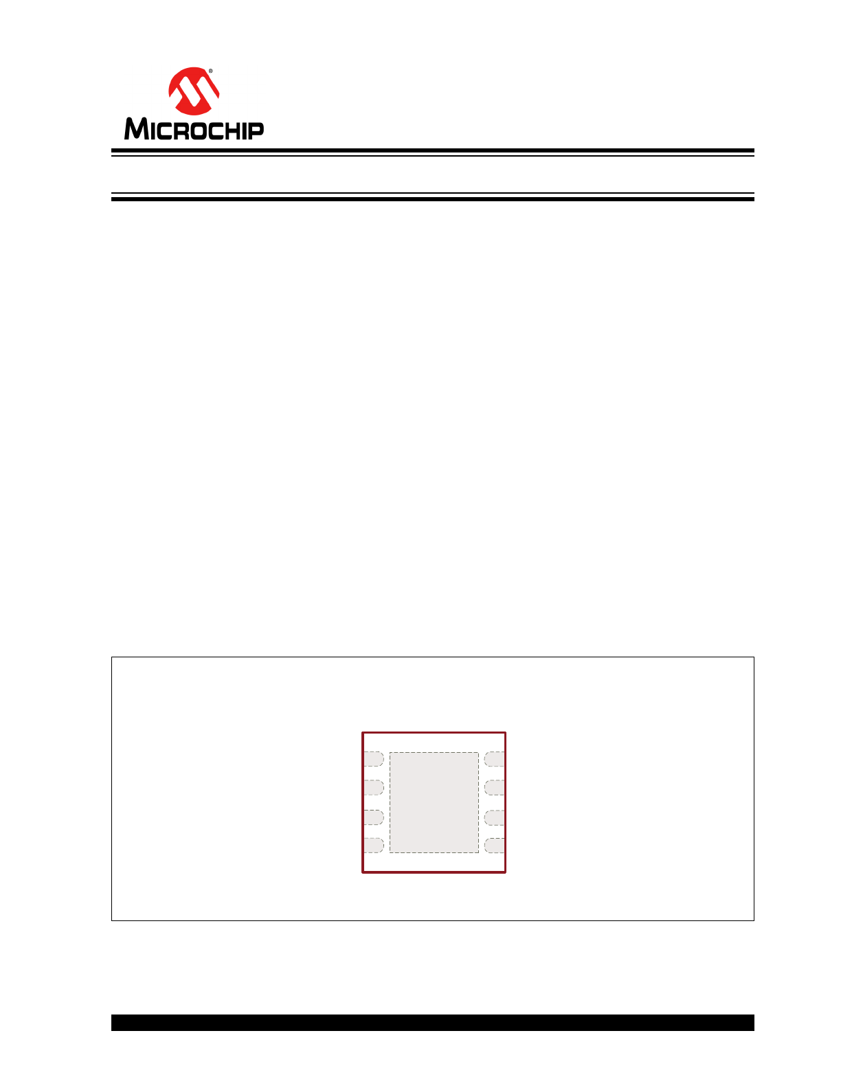
Package Type
8-lead DFN
(Top View)
See
Table 2-1
for pin information.
8
1
2
3
4
7
6
5
CS
VIN
GATE
RAMP
ADIM
GND
VDD
DIM
GND
Hysteretic Buck High-Brightness LED Driver with High-Side Current Sensing
AT9919
DS20005595A-page 2
2016 Microchip Technology Inc.
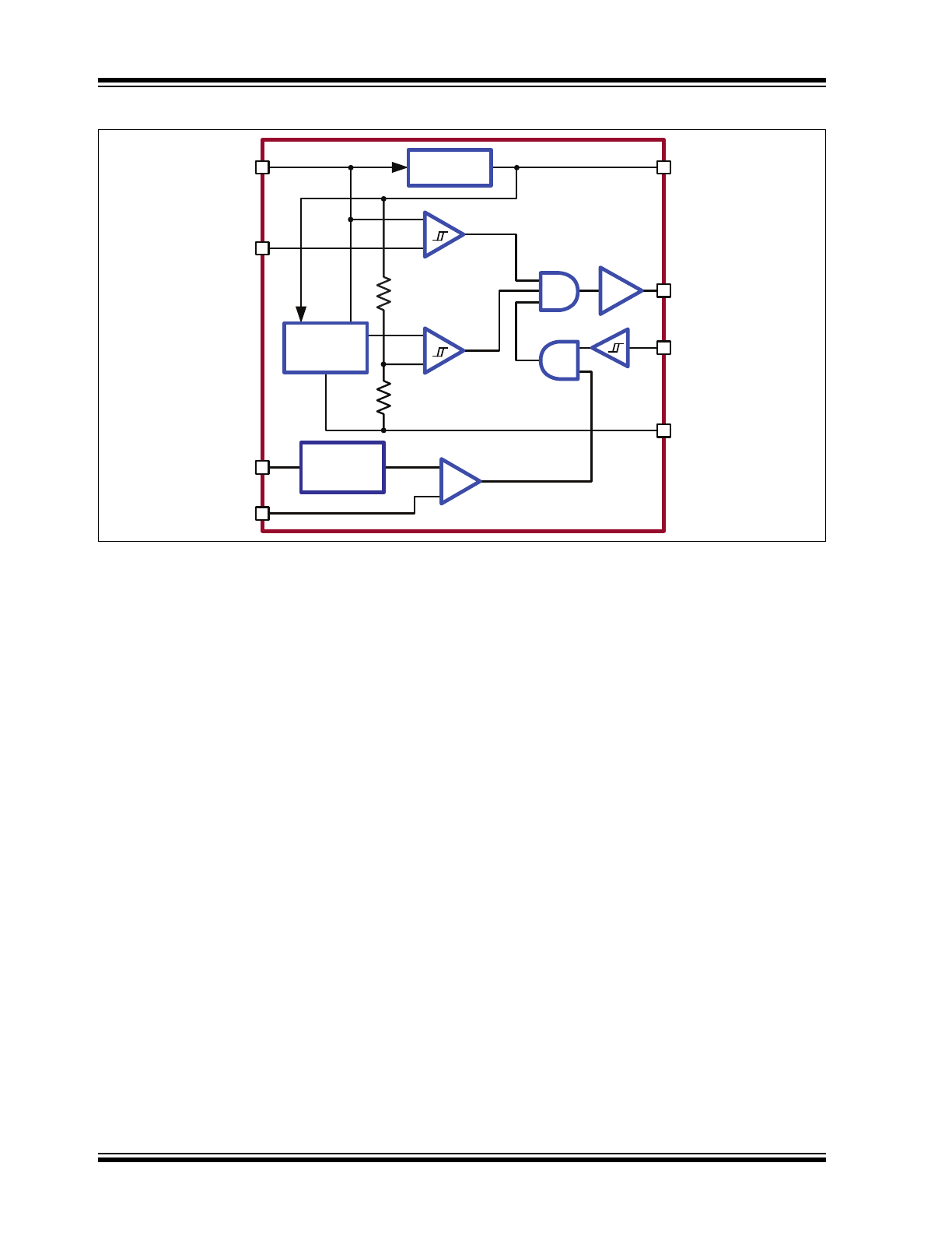
Functional Block Diagram
CURRENT
SENSE
COMPARATOR
UVLO
COMPARATOR
GATE
DRIVER
VIN
VDD
CS
RAMP
ADIM
GND
DIM
GATE
AT9919
PWM RAMP
0.1~1.9V
-
+
+
-
BANDGAP
REF
+
-
REGULATOR
2016 Microchip Technology Inc.
DS20005595A-page 3
AT9919
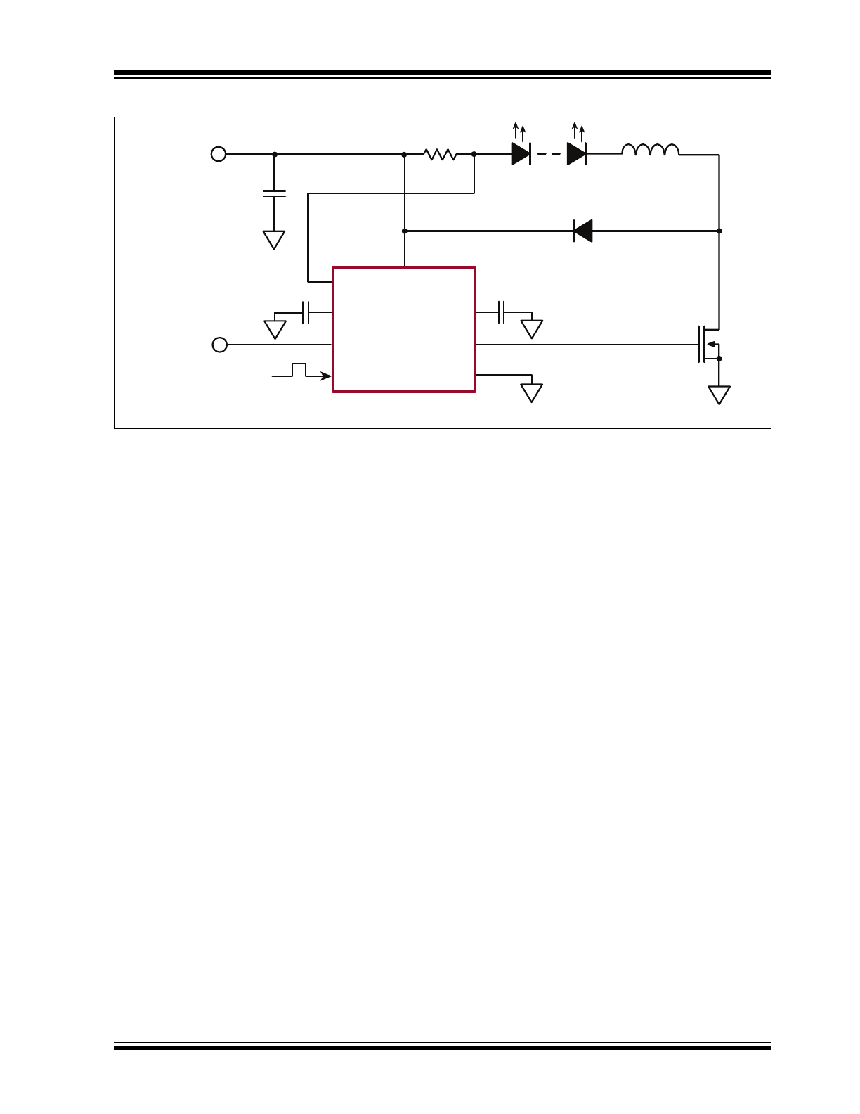
Typical Application
C
IN
0 - 2.0V
AT9919
VIN
VDD
GATE
GND
CS
RAMP
ADIM
DIM
R
SENSE
L
Circuit

AT9919
DS20005595A-page 4
2016 Microchip Technology Inc.
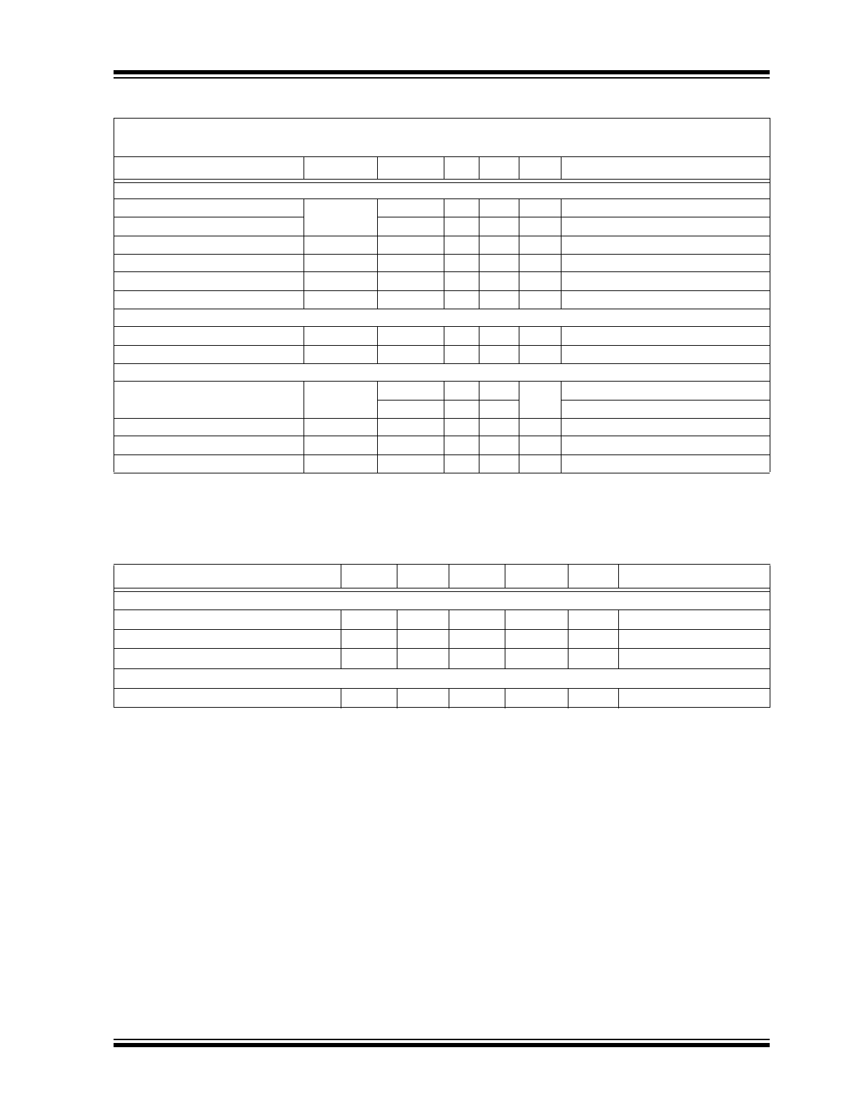
1.0
ELECTRICAL CHARACTERISTICS
Absolute Maximum Ratings†
V
IN
and CS to GND ...................................................................................................................................–0.3V to +45V
V
DD
, GATE, RAMP, DIM, ADIM to GND......................................................................................................–0.3V to +6V
CS to V
IN
.....................................................................................................................................................–1V to +0.3V
Operating Temperature Range............................................................................................................. –40°C to +125°C
Junction Temperature.............................................................................................................................................150°C
Storage Temperature Range ...................................................................................................................–65°C to 150°C
Continuous Power Dissipation (T
A
= +25°C) .......................................................................................................... 1.6W
† Notice: Stresses above those listed under “Absolute Maximum Ratings” may cause permanent damage to the
device. This is a stress rating only, and functional operation of the device at those or any other conditions above those
indicated in the operational sections of this specification is not intended. Exposure to maximum rating conditions for
extended periods may affect device reliability.
ELECTRICAL CHARACTERISTICS
Electrical Specifications: V
IN
= 12V, V
DIM
= V
DD
, V
RAMP
= GND, C
VDD
= 1 µF, R
CS
= 0.5Ω, T
A
= T
J
= –40ºC to
+125ºC (
Note 1
) unless otherwise noted.
Parameter
Sym.
Min.
Typ. Max.
Unit
Conditions
Input DC Supply Voltage Range
V
IN
4.5
—
40
V
DC input voltage
Internally Regulated Voltage
V
DD
4.5
—
5.5
V
V
IN
= 6V to 40V
Supply Current
I
IN
—
—
1.5
mA
GATE open
Shutdown Supply Current
I
IN, SDN
—
—
900
µA
DIM < 0.7V
Current Limit
I
IN, LIM
—
30
—
mA
V
IN
= 4.5V, V
DD
= 0V
—
8
—
V
IN
= 4.5V, V
DD
= 4V
Oscillator Frequency
f
OSC
—
—
2
MHz
V
DD
Undervoltage Lockout
Threshold
UVLO
—
—
4.5
V
V
DD
rising
V
DD
Undervoltage Lockout
Hysteresis
UVLO
HYST
—
500
—
mV
V
DD
falling
SENSE COMPARATOR
Sense Voltage Threshold High
V
CS(HI)
198
230
257
mV
(V
IN
– V
CS
) rising
Sense Voltage Threshold Low
V
CS(LO)
147
170
195
mV
(V
IN
– V
CS
) falling
Average Reference Voltage
V
CS(AVG)
186
200
214
mV
V
CS(AVG)
= 0.5V
CS(HI)
+ 0.5V
CS(LO)
Propagation Delay to Output
High
t
DPDH
—
70
—
ns
Falling edge of
V
IN
– V
CS
= V
RS(LO)
– 70 mV
Propagation Delay to Output
Low
t
DPDL
—
70
—
ns
Rising edge of
V
IN
– V
CS
= V
RS(HI)
+ 70 mV
Current Sense Input Current
I
CS
—
—
1
µA
V
IN
– V
CS
= 200 mV
Current Sense Threshold
Hysteresis
V
CS(HYST)
—
56
80
mV
DIM INPUT
Pin DIM Input High Voltage
V
IH
2.2
—
—
V
Pin DIM Input Low Voltage
V
IL
—
—
0.7
V
Turn-on Time
t
ON
—
100
—
ns
DIM rising edge to
V
GATE
= 0.5 x V
DD
, C
GATE
= 2 nF
Turn-off Time
t
OFF
—
100
—
ns
DIM falling edge to
V
GATE
= 0.5 x V
DD
, C
GATE
= 2 nF
Note 1:
Limits obtained by design and characterization.
2: For design guidance only
2016 Microchip Technology Inc.
DS20005595A-page 5
AT9919
GATE DRIVER
GATE Current, Source
I
GATE
0.3
0.5
—
A
V
GATE
= GND (
Note 2
)
GATE Current, Sink
0.7
1
—
A
V
GATE
= V
DD
(
Note 2
)
GATE Output Rise Time
T
RISE
—
40
55
ns
C
GATE
= 2 nF
GATE Output Fall Time
T
FALL
—
17
25
ns
C
GATE
= 2 nF
GATE High Output Voltage
V
GATE(HI)
V
DD
– 0.5
—
—
V
I
GATE
= 10 mA
GATE Low Output Voltage
V
GATE(LO)
—
—
0.5
V
I
GATE
= –10 mA
OVERTEMPERATURE PROTECTION
Over Temperature Trip Limit
T
OT
128
140
—
ºC
Note 2
Temperature Hysteresis
∆T
HYST
—
60
—
ºC
Note 2
ANALOG CONTROL OF PWM DIMMING
Dimming Frequency
f
RAMP
130
—
300
Hz
C
RAMP
= 47 nF
550
—
1250
C
RAMP
= 10 nF
RAMP Threshold, Low
V
LOW
—
0.1
—
V
RAMP Threshold, High
V
HIGH
1.8
—
2.1
V
ADIM Offset Voltage
V
OS
–35
—
+35
mV
TEMPERATURE SPECIFICATIONS
Parameter
Sym.
Min.
Typ.
Max.
Unit
Conditions
TEMPERATURE RANGE
Operating Temperature
T
A
–40
—
+125
°C
Junction Temperature
T
J
—
—
+150
°C
Storage Temperature
T
S
–65
—
+150
°C
PACKAGE THERMAL RESISTANCE
8-lead DFN
JA
—
+37
—
°C/W
ELECTRICAL CHARACTERISTICS (CONTINUED)
Electrical Specifications: V
IN
= 12V, V
DIM
= V
DD
, V
RAMP
= GND, C
VDD
= 1 µF, R
CS
= 0.5Ω, T
A
= T
J
= –40ºC to
+125ºC (
Note 1
) unless otherwise noted.
Parameter
Sym.
Min.
Typ. Max.
Unit
Conditions
Note 1:
Limits obtained by design and characterization.
2: For design guidance only

AT9919
DS20005595A-page 6
2016 Microchip Technology Inc.
2.0
PIN DESCRIPTION
The details on the pins of AT9919 are listed on
Table 2-1
. Refer to
Package Type
for the location of
pins.
TABLE 2-1:
PIN FUNCTION TABLE
Pin Number
Pin Name
Description
1
CS
Current sense input. Senses LED string current.
2
VIN
Input voltage 4.5V to 40V DC
3
RAMP
Analog PWM dimming ramp output
4
ADIM
Analog 0V~2V signal input for analog control of PWM dimming
5
DIM
PWM signal input
6
VDD
Internally regulated supply voltage. Connect a capacitor from VDD to ground.
7
GND
Device ground
8
GATE
Drives GATE of the external MOSFET
TAB
GND
Must be wired to pin 7 on PCB
2016 Microchip Technology Inc.
DS20005595A-page 7
AT9919
3.0
APPLICATION INFORMATION
3.1
General Description
The AT9919 is a step-down constant-current
high-brightness LED (HB LED) driver. The device
operates from a 4.5V to 40V input voltage range and
provides the gate drive output to an external N-channel
MOSFET. A high-side current sense resistor sets the
output current, and a dedicated PWM dimming input
(DIM) allows for a wide range of dimming duty ratios.
The PWM dimming could also be achieved by applying
a DC voltage between 0V and 2V to the analog
dimming input (ADIM). In this case, the dimming
frequency can be programmed using a single capacitor
at the RAMP pin. The high-side current sensing
scheme minimizes the number of external components
while delivering LED current with a ±8% accuracy,
using a 1% sense resistor.
3.2
Undervoltage Lockout (UVLO)
The AT9919 includes a 3.7V UVLO with 500 mV
hysteresis. When V
IN
falls below 3.7V, GATE goes low,
turning off the external N-channel MOSFET. GATE
goes high once V
IN
is 4.5V or higher.
3.3
5V Regulator
V
DD
is the output of a 5V regulator capable of sourcing
8 mA. Bypass V
DD
to GND with a 1 µF capacitor.
3.4
DIM Input
The AT9919 allows dimming with a PWM signal at the
DIM input. A logic level below 0.7V at DIM forces the
GATE
OUTPUT
low, turning off the LED current. To turn
on the LED current, the logic level at DIM must be at
least 2.2V.
3.5
ADIM and RAMP Inputs
The PWM dimming scheme can also be implemented
by applying an analog control signal to the ADIM pin. If
an analog control signal of 0V~2.0V is applied to ADIM,
the device compares this analog input to a voltage
ramp to pulse width modulate the LED current.
Connecting an external capacitor to RAMP programs
the PWM dimming ramp frequency. See
Equation 3-1
.
EQUATION 3-1:
f
PWM
1
C
RAMP
120k
-----------------------------------------
=
The DIM and ADIM inputs can be used simultaneously.
In such case, a f
PWM(MAX)
lower than the frequency of
the dimming signal at DIM
must be selected. The
smaller dimming duty cycle of ADIM and DIM will
determine the GATE signal.
When the analog control of PWM dimming feature is
not used, RAMP must be wired to GND and ADIM
should be connected to V
DD
.
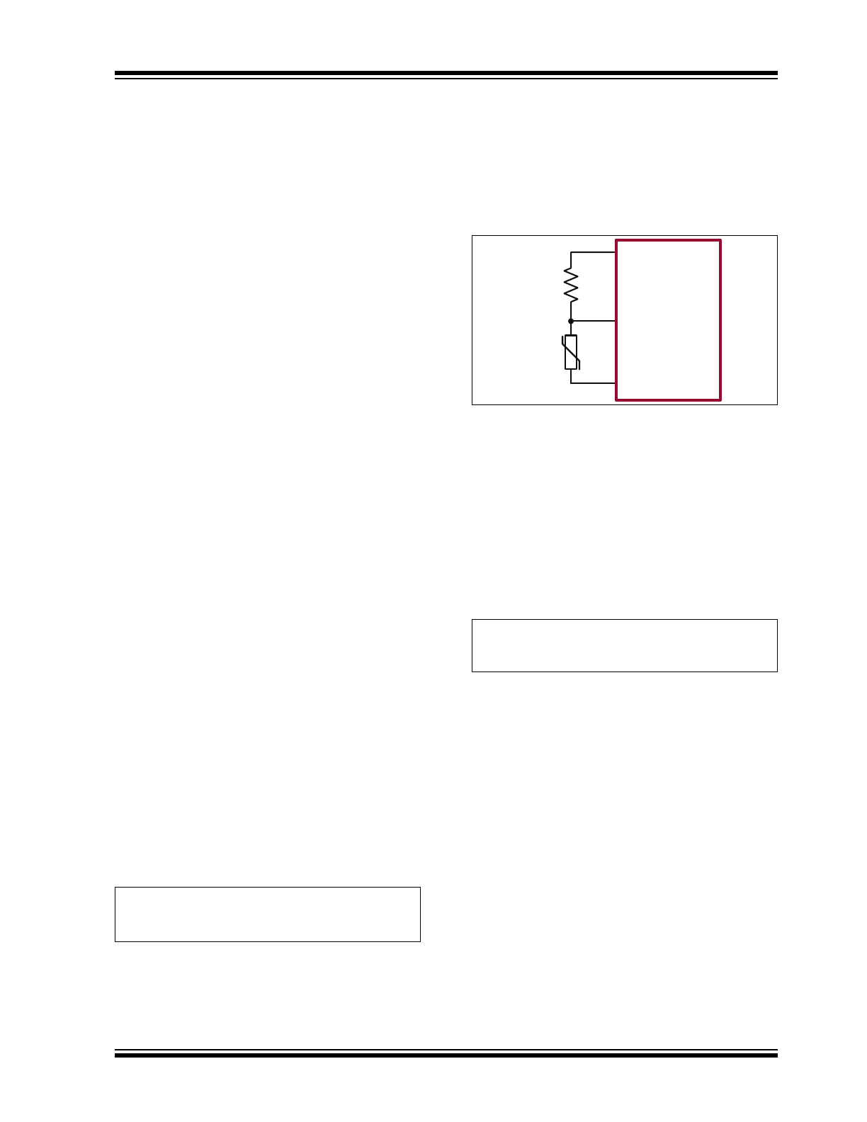
One possible application of the ADIM feature may
include protection of the LED load from
overtemperature by connecting an NTC thermistor to
ADIM as shown in
Figure 3-1
.
NTC
VDD
ADIM
GND
AT9919
FIGURE 3-1:
Overtemperature Protection
using ADIM Pin.
3.6
Setting LED Current with the
External Resistor (R
SENSE
)
The output current in the LED is determined by the
external current sense resistor (R
SENSE
) connected
between V
IN
and CS. Disregarding the effect of the
propagation delays, the sense resistor can be
calculated as seen in
Equation 3-2
.
EQUATION 3-2:
R
SENSE
1
2
---
V
RS HI
V
RS LO
+
I
LED
---------------------------------------------
200mV
I
LED
-----------------
=
3.7
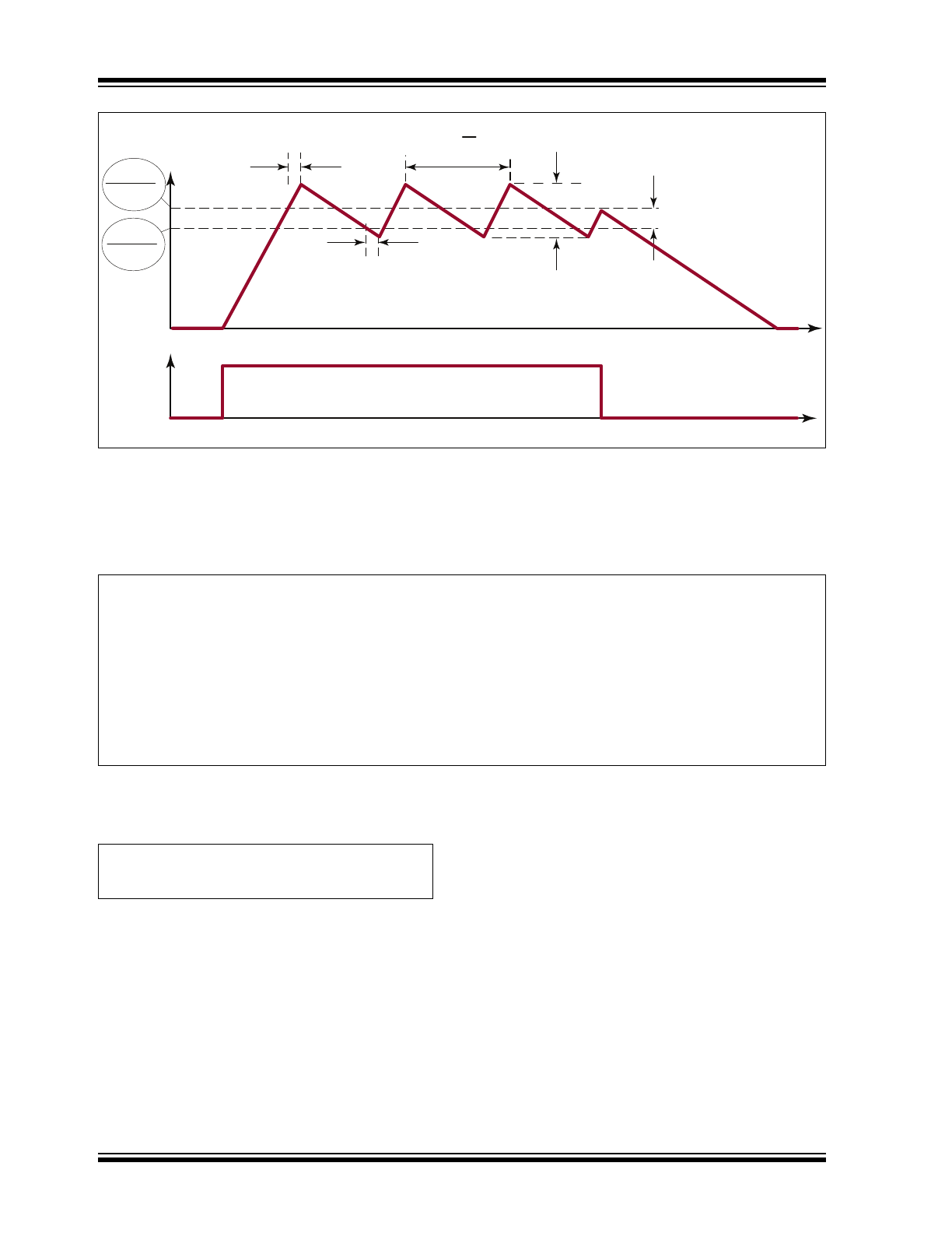
Selecting Buck Inductor (L)
The AT9919 regulates the LED output current using an
input comparator with hysteresis. (See
Figure 3-2
.) As
the current through the inductor ramps up, and the
voltage across the sense resistor reaches the upper
threshold, the voltage at GATE goes low, turning off the
external MOSFET. The MOSFET turns on again when
the inductor current ramps down through the
freewheeling diode until the voltage across the sense
resistor equals the lower threshold.
AT9919
DS20005595A-page 8
2016 Microchip Technology Inc.
FIGURE 3-2:
Inductor Current Waveform.
t
t
I
LED
V
DIM
V
RS(HI)
R
SENSE
V
RS(LO)
R
SENSE
t
DPDL
t
DPDH
T
S
=
1
f
S
ΔI
ΔI
O
Equation 3-3
shows how to determine the inductor
value for a desired operating frequency (f
S
)
.
EQUATION 3-3:
L
V
IN
V
OUT
–
V
OUT
f
S
V
IN
I
O
------------------------------------------------------
V
IN
V
OUT
–
t
DPDL
I
O
-------------------------------------------------------
–
V
OUT
t
DPDH
I
O
------------------------------
–
=
Where:
I
O
V
RS HI
V
RS LO
–
R
SENSE
--------------------------------------------
=
and t
DPDL
and t
DPDH
are the propagation delays.
Note that the current ripple (∆I) in the inductor (L) is greater than ∆I
O
.
The current ripple in the inductor (L) can be calculated
with
Equation 3-4
.
EQUATION 3-4:
I
I
O
V
IN
V
OUT
–
t
DPDL
L
-------------------------------------------------------
V
OUT
t
DPDH
L
------------------------------
+
+
=
For proper inductor selection, note that the maximum
switching frequency occurs at the highest V
IN
and
V
OUT
= V
IN
/2.
3.8
MOSFET Selection
MOSFET selection is based on the maximum input
operating voltage V
IN
, output current I
LED
and
operating switching frequency. Choose a MOSFET that
has a higher breakdown voltage than the maximum
operation voltage, low R
DS(ON)
and low total charge for
better efficiency. MOSFET threshold voltage must be
adequate when operated at the low end of the input
voltage operating range.
3.9
Freewheeling Diode Selection
The forward voltage of the freewheeling diode should
be as low as possible for better efficiency. A Schottky
diode is a good choice as long as the breakdown
voltage is high enough to withstand the maximum
operating voltage. The forward current rating of the
diode must be at least equal to the maximum LED
current.
3.10
LED Current Ripple
The LED current ripple is equal to the inductor current
ripple. In cases when a lower LED current ripple is
needed, a capacitor can be placed across the LED
terminals.

2016 Microchip Technology Inc.
DS20005595A-page 9
AT9919
3.11
PCB Layout Guidelines
Careful PCB layout is critical to achieving low switching
losses and stable operation. Use a multilayer board
whenever possible for better noise immunity. Minimize
ground noise by connecting high-current ground
returns, the input bypass capacitor ground lead and the
output filter ground lead to a single point (star ground
configuration). The fast di/dt loop is composed of the
input capacitor C
IN
, the freewheeling diode and the
MOSFET. To minimize noise interaction, this loop area
should be as small as possible. Place R
SENSE
as close
as possible to the input filter and V
IN
. For better noise
immunity, a Kelvin connection is strongly
recommended between CS and R
SENSE
. Connect the
exposed tab of the IC to a large area ground plane for
improved power dissipation.
AT9919
DS20005595A-page 10
2016 Microchip Technology Inc.
4.0
PACKAGING INFORMATION
4.1
Package Marking Information
Legend: XX...X
Product Code or Customer-specific information
Y
Year code (last digit of calendar year)
YY
Year code (last 2 digits of calendar year)
WW
Week code (week of January 1 is week ‘01’)
NNN
Alphanumeric traceability code
Pb-free JEDEC
®
designator for Matte Tin (Sn)
*
This package is Pb-free. The Pb-free JEDEC designator ( )
can be found on the outer packaging for this package.
Note:
In the event the full Microchip part number cannot be marked on one line, it will
be carried over to the next line, thus limiting the number of available
characters for product code or customer-specific information. Package may or
not include the corporate logo.
3
e
3
e
8-lead DFN
Example
NNN
YYWW
XXXX
373
1612
9919