
Features
•
High-performance, Low-power AVR
®
8-bit Microcontroller
•
Advanced RISC Architecture
– 133 Powerful Instructions – Most Single Clock Cycle Execution
– 32 x 8 General Purpose Working Registers + Peripheral Control Registers
– Fully Static Operation
– Up to 16 MIPS Throughput at 16 MHz
– On-chip 2-cycle Multiplier
•
Non volatile Program and Data Memories
– 32K/64K/128K Bytes of In-System Reprogrammable Flash (AT90CAN32/64/128)
• Endurance: 10,000 Write/Erase Cycles
– Optional Boot Code Section with Independent Lock Bits
• Selectable Boot Size: 1K Bytes, 2K Bytes, 4K Bytes or 8K Bytes
• In-System Programming by On-Chip Boot Program (CAN, UART, ...)
• True Read-While-Write Operation
– 1K/2K/4K Bytes EEPROM (Endurance: 100,000 Write/Erase Cycles) (AT90CAN32/64/128)
– 2K/4K/4K Bytes Internal SRAM (AT90CAN32/64/128)
– Up to 64K Bytes Optional External Memory Space
– Programming Lock for Software Security
•
JTAG (IEEE std. 1149.1 Compliant) Interface
– Boundary-scan Capabilities According to the JTAG Standard
– Programming Flash (Hardware ISP), EEPROM, Lock & Fuse Bits
– Extensive On-chip Debug Support
•
CAN Controller 2.0A & 2.0B - ISO 16845 Certified
(1)
– 15 Full Message Objects with Separate Identifier Tags and Masks
– Transmit, Receive, Automatic Reply and Frame Buffer Receive Modes
– 1Mbits/s Maximum Transfer Rate at 8 MHz
– Time stamping, TTC & Listening Mode (Spying or Autobaud)
•
Peripheral Features
– Programmable Watchdog Timer with On-chip Oscillator
– 8-bit Synchronous Timer/Counter-0
• 10-bit Prescaler
• External Event Counter
• Output Compare or 8-bit PWM Output
– 8-bit Asynchronous Timer/Counter-2
• 10-bit Prescaler
• External Event Counter
• Output Compare or 8-Bit PWM Output
• 32Khz Oscillator for RTC Operation
– Dual 16-bit Synchronous Timer/Counters-1 & 3
• 10-bit Prescaler
• Input Capture with Noise Canceler
• External Event Counter
• 3-Output Compare or 16-Bit PWM Output
• Output Compare Modulation
– 8-channel, 10-bit SAR ADC
• 8 Single-ended Channels
• 7 Differential Channels
• 2 Differential Channels With Programmable Gain at 1x, 10x, or 200x
– On-chip Analog Comparator
– Byte-oriented Two-wire Serial Interface
– Dual Programmable Serial USART
– Master/Slave SPI Serial Interface
• Programming Flash (Hardware ISP)
•
Special Microcontroller Features
– Power-on Reset and Programmable Brown-out Detection
– Internal Calibrated RC Oscillator
– 8 External Interrupt Sources
– 5 Sleep Modes: Idle, ADC Noise Reduction, Power-save, Power-down & Standby
– Software Selectable Clock Frequency
– Global Pull-up Disable
•
I/O and Packages
– 53 Programmable I/O Lines
– 64-lead TQFP and 64-lead QFN
•
Operating Voltages: 2.7 - 5.5V
•
Operating temperature: Industrial (-40°C to +85°C)
•
Maximum Frequency: 8 MHz at 2.7V, 16 MHz at 4.5V
Note:
1.
Details on
section 19.4.3 on page 242
.
Rev. 7679HS–CAN–08/08
8-bit
Microcontroller
with
32K/64K/128K
Bytes of
ISP Flash
and
CAN Controller
AT90CAN32
AT90CAN64
AT90CAN128
Summary

2
7679HS–CAN–08/08
AT90CAN32/64/128
1.
Description
1.1
Comparison Between AT90CAN32, AT90CAN64 and AT90CAN128
AT90CAN32, AT90CAN64 and AT90CAN128 are hardware and software compatible. They dif-
fer only in memory sizes as shown in
Table 1-1
.
1.2
Part Description
The AT90CAN32/64/128 is a low-power CMOS 8-bit microcontroller based on the AVR
enhanced RISC architecture. By executing powerful instructions in a single clock cycle, the
AT90CAN32/64/128 achieves throughputs approaching 1 MIPS per MHz allowing the system
designer to optimize power consumption versus processing speed.
The AVR core combines a rich instruction set with 32 general purpose working registers. All 32
registers are directly connected to the Arithmetic Logic Unit (ALU), allowing two independent
registers to be accessed in one single instruction executed in one clock cycle. The resulting
architecture is more code efficient while achieving throughputs up to ten times faster than con-
ventional CISC microcontrollers.
The AT90CAN32/64/128 provides the following features: 32K/64K/128K bytes of In-System Pro-
grammable Flash with Read-While-Write capabilities, 1K/2K/4K bytes EEPROM, 2K/4K/4K
bytes SRAM, 53 general purpose I/O lines, 32 general purpose working registers, a CAN con-
troller, Real Time Counter (RTC), four flexible Timer/Counters with compare modes and PWM, 2
USARTs, a byte oriented Two-wire Serial Interface, an 8-channel 10-bit ADC with optional differ-
ential input stage with programmable gain, a programmable Watchdog Timer with Internal
Oscillator, an SPI serial port, IEEE std. 1149.1 compliant JTAG test interface, also used for
accessing the On-chip Debug system and programming and five software selectable power sav-
ing modes.
The Idle mode stops the CPU while allowing the SRAM, Timer/Counters, SPI/CAN ports and
interrupt system to continue functioning. The Power-down mode saves the register contents but
freezes the Oscillator, disabling all other chip functions until the next interrupt or Hardware
Reset. In Power-save mode, the asynchronous timer continues to run, allowing the user to main-
tain a timer base while the rest of the device is sleeping. The ADC Noise Reduction mode stops
the CPU and all I/O modules except Asynchronous Timer and ADC, to minimize switching noise
during ADC conversions. In Standby mode, the Crystal/Resonator Oscillator is running while the
rest of the device is sleeping. This allows very fast start-up combined with low power
consumption.
The device is manufactured using Atmel’s high-density nonvolatile memory technology. The On-
chip ISP Flash allows the program memory to be reprogrammed in-system through an SPI serial
interface, by a conventional nonvolatile memory programmer, or by an On-chip Boot program
running on the AVR core. The boot program can use any interface to download the application
program in the application Flash memory. Software in the Boot Flash section will continue to run
while the Application Flash section is updated, providing true Read-While-Write operation. By
Table 1-1.
Memory Size Summary
Device
Flash
EEPROM
RAM
AT90CAN32
32K Bytes
1K Byte
2K Bytes
AT90CAN64
64K Bytes
2K Bytes
4K Bytes
AT90CAN128
128K Bytes
4K Byte
4K Bytes

3
7679HS–CAN–08/08
AT90CAN32/64/128
combining an 8-bit RISC CPU with In-System Self-Programmable Flash on a monolithic chip,
the Atmel AT90CAN32/64/128 is a powerful microcontroller that provides a highly flexible and
cost effective solution to many embedded control applications.
The AT90CAN32/64/128 AVR is supported with a full suite of program and system development
tools including: C compilers, macro assemblers, program debugger/simulators, in-circuit emula-
tors, and evaluation kits.
1.3
Disclaimer
Typical values contained in this datasheet are based on simulations and characterization of
other AVR microcontrollers manufactured on the same process technology. Min and Max values
will be available after the device is characterized.
4
7679HS–CAN–08/08
AT90CAN32/64/128
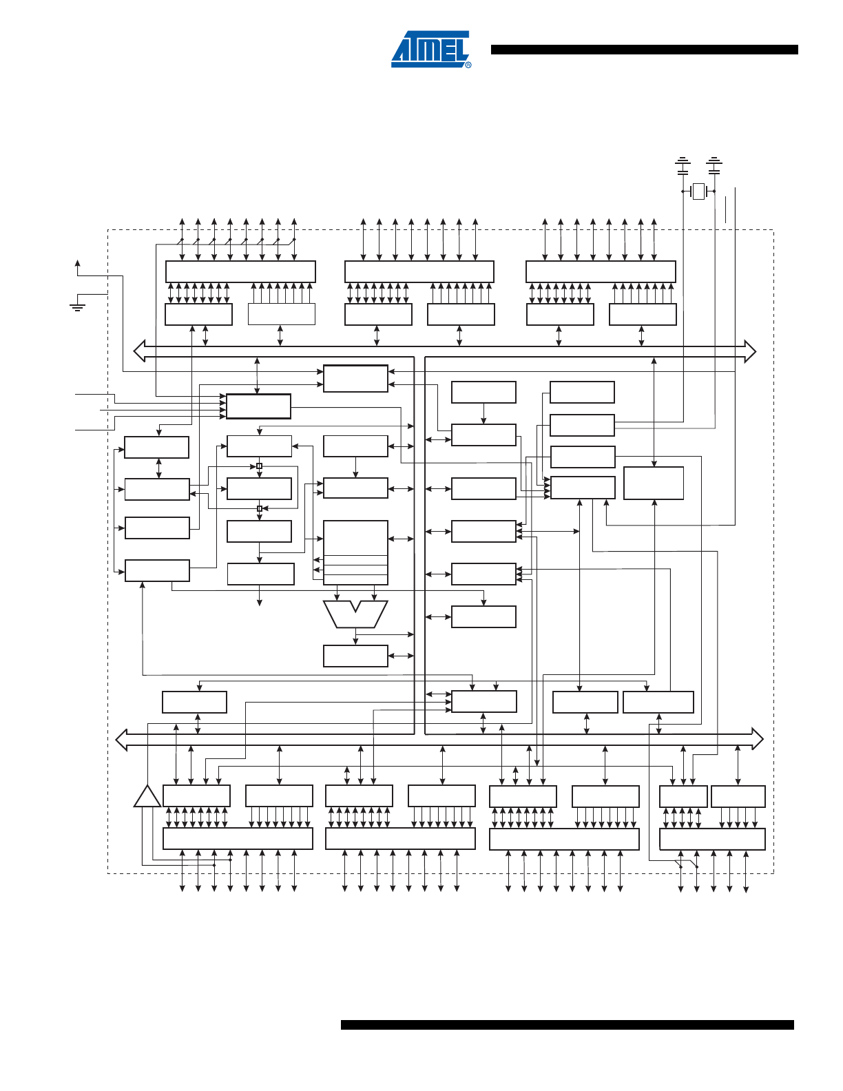
1.4
Block Diagram
Figure 1-1.
Block Diagram
PROGRAM
COUNTER
STACK
POINTER
PROGRAM
FLASH
MCU CONTROL
REGISTER
SRAM
GENERAL
PURPOSE
REGISTERS
INSTRUCTION
REGISTER
TIMER/
COUNTERS
INSTRUCTION
DECODER
DATA DIR.
REG. PORTB
DATA DIR.
REG. PORTE
DATA DIR.
REG. PORTA
DATA DIR.
REG. PORTD
DATA REGISTER
PORTB
DATA REGISTER
PORTE
DATA REGISTER
PORTA
DATA REGISTER
PORTD
INTERRUPT
UNIT
EEPROM
SPI
USART0
STATUS
REGISTER
Z
Y
X
ALU
PORTB DRIVERS
PORTE DRIVERS
PORTA DRIVERS
PORTF DRIVERS
PORTD DRIVERS
PORTC DRIVERS
PB7 - PB0
PE7 - PE0
PA7 - PA0
PF7 - PF0
RESET
VCC
AGND
GND
AREF
XT
AL1
XT
AL2
CONTROL
LINES
+
-
ANALOG
COMP
ARA
T
O
R
PC7 - PC0
INTERNAL
OSCILLATOR
WATCHDOG
TIMER
8-BIT DATA BUS
AVCC
USART1
TIMING AND
CONTROL
OSCILLATOR
OSCILLATOR
CALIB. OSC
DATA DIR.
REG. PORTC
DATA REGISTER
PORTC
ON-CHIP DEBUG
JTAG TAP
PROGRAMMING
LOGIC
BOUNDARY-
SCAN
DATA DIR.
REG. PORTF
DATA REGISTER
PORTF
ADC
POR - BOD
RESET
PD7 - PD0
DATA DIR.
REG. PORTG
DATA REG.
PORTG
PORTG DRIVERS
PG4 - PG0
TWO-WIRE SERIAL
INTERFACE
CAN
CONTROLLER
5
7679HS–CAN–08/08
AT90CAN32/64/128
1.5
Pin Configurations
Figure 1-2.
Pinout AT90CAN32/64/128 - TQFP
PC0 (A8)
VCC
GND
PF0 (ADC0)
PF7 (ADC7 / TDI)
PF1 (ADC1)
PF2 (ADC2)
PF3 (ADC3)
PF4 (ADC4 / TCK)
PF5 (ADC5 / TMS)
PF6 (ADC6 / TDO)
AREF
GND
AVCC
17
61
60
18
59
20
58
19
21
57
22
56
23
55
24
54
25
53
26
52
27
51
29
28
50
49
32
31
30
(RXD0 / PDI) PE0
(TXD0 / PDO) PE1
(XCK0 / AIN0) PE2
(OC3A / AIN1) PE3
(OC3B / INT4) PE4
(OC3C / INT5) PE5
(T3 / INT6) PE6
(ICP3 / INT7) PE7
(SS) PB0
(SCK) PB1
(MOSI) PB2
(MISO) PB3
(OC2A) PB4
(OC0A / OC1C) PB7
(TOSC2 ) PG3
(OC1B) PB6
(TOSC1 ) PG4
(OC1A) PB5
PC1 (A9)
(T0) PD7
PC2 (A10)
PC3 (A11)
PC4 (A12)
PC5 (A13)
PC6 (A14)
PC7 (A15 / CLKO)
PA7 (AD7)
PG2 (ALE)
PA6 (AD6)
PA5 (AD5)
PA4 (AD4)
PA3 (AD3)
PA0 (AD0)
PA1 (AD1)
PA2 (AD2)
(RXCAN / T1) PD6
(TXCAN / XCK1) PD5
(ICP1) PD4
(TXD1 / INT3) PD3
(RXD1 / INT2) PD2
(SDA / INT1) PD1
(SCL / INT0) PD0
XTAL1
XTAL2
RESET
GND
VCC
PG1 (RD)
PG0 (WR)
2
3
1
4
5
6
7
8
9
10
11
12
13
14
16
15
64
63
62
47
46
48
45
44
43
42
41
40
39
38
37
36
35
33
34
(2)
(2)
NC = Do not connect (May be used in future devices)
(1)
Timer2 Oscillator
(2)
NC
(1)
(64-lead TQFP top view)
INDEX CORNER
6
7679HS–CAN–08/08
AT90CAN32/64/128
Figure 1-3.
Pinout AT90CAN32/64/128 - QFN
Note:
The large center pad underneath the QFN package is made of metal and internally connected to
GND. It should be soldered or glued to the board to ensure good mechanical stability. If the center
pad is left unconnected, the package might loosen from the board.
1.6
Pin Descriptions
1.6.1
VCC
Digital supply voltage.
1.6.2
GND
Ground.
NC = Do not connect (May be used in future devices)
(1)
Timer2 Oscillator
(2)
PC0 (A8)
VCC
GND
PF0 (ADC0)
PF7 (ADC7 / TDI)
PF1 (ADC1)
PF2 (ADC2)
PF3 (ADC3)
PF4 (ADC4 / TCK)
PF5 (ADC5 / TMS)
PF6 (ADC6 / TDO)
AREF
GND
AVCC
(RXD0 / PDI) PE0
(TXD0 / PDO) PE1
(XCK0 / AIN0) PE2
(OC3A / AIN1) PE3
(OC3B / INT4) PE4
(OC3C / INT5) PE5
(T3 / INT6) PE6
(ICP3 / INT7) PE7
(SS) PB0
(SCK) PB1
(MOSI) PB2
(MISO) PB3
(OC2A) PB4
(OC0A / OC1C) PB7
(TOSC2 ) PG3
(OC1B) PB6
(TOSC1 ) PG4
(OC1A) PB5
PC1 (A9)
(T0) PD7
PC2 (A10)
PC3 (A11)
PC4 (A12)
PC5 (A13)
PC6 (A14)
PC7 (A15 / CLKO)
PA7 (AD7)
PG2 (ALE)
PA6 (AD6)
PA5 (AD5)
PA4 (AD4)
PA3 (AD3)
PA0 (AD0)
PA1 (AD1)
PA2 (AD2)
(RXCAN / T1) PD6
(TXCAN / XCK1) PD5
(ICP1) PD4
(TXD1 / INT3) PD3
(RXD1 / INT2) PD2
(SDA / INT1) PD1
(SCL / INT0) PD0
XTAL1
XTAL2
RESET
GND
VCC
PG1 (RD)
PG0 (WR)
2
3
1
4
5
6
7
8
9
10
11
12
13
14
16
33
15
47
46
48
45
44
43
42
41
40
39
38
37
36
35
34
(2)
(2)
NC
(1)
17
18
20
19
21
22
23
24
25
26
27
29
28
32
31
30
52
51
50
49
64
63
62
53
61
60
59
58
57
56
55
54
(64-lead QFN top view)
INDEX CORNER

7
7679HS–CAN–08/08
AT90CAN32/64/128
1.6.3
Port A (PA7..PA0)
Port A is an 8-bit bi-directional I/O port with internal pull-up resistors (selected for each bit). The
Port A output buffers have symmetrical drive characteristics with both high sink and source
capability. As inputs, Port A pins that are externally pulled low will source current if the pull-up
resistors are activated. The Port A pins are tri-stated when a reset condition becomes active,
even if the clock is not running.
Port A also serves the functions of various special features of the AT90CAN32/64/128 as listed
on
page 74
.
1.6.4
Port B (PB7..PB0)
Port B is an 8-bit bi-directional I/O port with internal pull-up resistors (selected for each bit). The
Port B output buffers have symmetrical drive characteristics with both high sink and source
capability. As inputs, Port B pins that are externally pulled low will source current if the pull-up
resistors are activated. The Port B pins are tri-stated when a reset condition becomes active,
even if the clock is not running.
Port B also serves the functions of various special features of the AT90CAN32/64/128 as listed
on
page 76
.
1.6.5
Port C (PC7..PC0)
Port C is an 8-bit bi-directional I/O port with internal pull-up resistors (selected for each bit). The
Port C output buffers have symmetrical drive characteristics with both high sink and source
capability. As inputs, Port C pins that are externally pulled low will source current if the pull-up
resistors are activated. The Port C pins are tri-stated when a reset condition becomes active,
even if the clock is not running.
Port C also serves the functions of special features of the AT90CAN32/64/128 as listed on
page
78
.
1.6.6
Port D (PD7..PD0)
Port D is an 8-bit bi-directional I/O port with internal pull-up resistors (selected for each bit). The
Port D output buffers have symmetrical drive characteristics with both high sink and source
capability. As inputs, Port D pins that are externally pulled low will source current if the pull-up
resistors are activated. The Port D pins are tri-stated when a reset condition becomes active,
even if the clock is not running.
Port D also serves the functions of various special features of the AT90CAN32/64/128 as listed
on
page 80
.
1.6.7
Port E (PE7..PE0)
Port E is an 8-bit bi-directional I/O port with internal pull-up resistors (selected for each bit). The
Port E output buffers have symmetrical drive characteristics with both high sink and source
capability. As inputs, Port E pins that are externally pulled low will source current if the pull-up
resistors are activated. The Port E pins are tri-stated when a reset condition becomes active,
even if the clock is not running.
Port E also serves the functions of various special features of the AT90CAN32/64/128 as listed
on
page 83
.
1.6.8
Port F (PF7..PF0)
Port F serves as the analog inputs to the A/D Converter.

8
7679HS–CAN–08/08
AT90CAN32/64/128
Port F also serves as an 8-bit bi-directional I/O port, if the A/D Converter is not used. Port pins
can provide internal pull-up resistors (selected for each bit). The Port F output buffers have sym-
metrical drive characteristics with both high sink and source capability. As inputs, Port F pins
that are externally pulled low will source current if the pull-up resistors are activated. The Port F
pins are tri-stated when a reset condition becomes active, even if the clock is not running.
Port F also serves the functions of the JTAG interface. If the JTAG interface is enabled, the pull-
up resistors on pins PF7(TDI), PF5(TMS), and PF4(TCK) will be activated even if a reset occurs.
1.6.9
Port G (PG4..PG0)
Port G is a 5-bit I/O port with internal pull-up resistors (selected for each bit). The Port G output
buffers have symmetrical drive characteristics with both high sink and source capability. As
inputs, Port G pins that are externally pulled low will source current if the pull-up resistors are
activated. The Port G pins are tri-stated when a reset condition becomes active, even if the clock
is not running.
Port G also serves the functions of various special features of the AT90CAN32/64/128 as listed
on
page 88
.
1.6.10
RESET
Reset input. A low level on this pin for longer than the minimum pulse length will generate a
reset. The minimum pulse length is given in characteristics. Shorter pulses are not guaranteed
to generate a reset. The I/O ports of the AVR are immediately reset to their initial state even if
the clock is not running. The clock is needed to reset the rest of the AT90CAN32/64/128.
1.6.11
XTAL1
Input to the inverting Oscillator amplifier and input to the internal clock operating circuit.
1.6.12
XTAL2
Output from the inverting Oscillator amplifier.
1.6.13
AVCC
AVCC is the supply voltage pin for the A/D Converter on Port F. It should be externally con-
nected to V
CC
, even if the ADC is not used. If the ADC is used, it should be connected to V
CC
through a low-pass filter.
1.6.14
AREF
This is the analog reference pin for the A/D Converter.
2.
About Code Examples
This documentation contains simple code examples that briefly show how to use various parts of
the device. These code examples assume that the part specific header file is included before
compilation. Be aware that not all C compiler vendors include bit definitions in the header files
and interrupt handling in C is compiler dependent. Please confirm with the C compiler documen-
tation for more details.
9
7679HS–CAN–08/08
AT90CAN32/64/128
3.
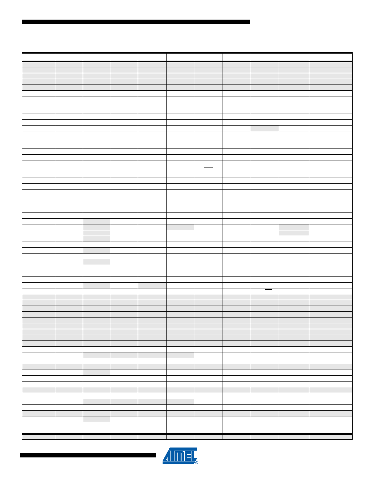
Register Summary
Address
Name
Bit 7
Bit 6
Bit 5
Bit 4
Bit 3
Bit 2
Bit 1
Bit 0
Page
(0xFF)
Reserved
(0xFE)
Reserved
(0xFD)
Reserved
(0xFC)
Reserved
(0xFB)
Reserved
(0xFA)
CANMSG
MSG 7
MSG 6
MSG 5
MSG 4
MSG 3
MSG 2
MSG 1
MSG 0
page 266
(0xF9)
CANSTMH
TIMSTM15
TIMSTM14
TIMSTM13
TIMSTM12
TIMSTM11
TIMSTM10
TIMSTM9
TIMSTM8
page 266
(0xF8)
CANSTML
TIMSTM7
TIMSTM6
TIMSTM5
TIMSTM4
TIMSTM3
TIMSTM2
TIMSTM1
TIMSTM0
page 266
(0xF7)
CANIDM1
IDMSK28
IDMSK27
IDMSK26
IDMSK25
IDMSK24
IDMSK23
IDMSK22
IDMSK21
page 265
(0xF6)
CANIDM2
IDMSK20
IDMSK19
IDMSK18
IDMSK17
IDMSK16
IDMSK15
IDMSK14
IDMSK13
page 265
(0xF5)
CANIDM3
IDMSK12
IDMSK11
IDMSK10
IDMSK9
IDMSK8
IDMSK7
IDMSK6
IDMSK5
page 265
(0xF4)
CANIDM4
IDMSK4
IDMSK3
IDMSK2
IDMSK1
IDMSK0
RTRMSK
–
IDEMSK
page 265
(0xF3)
CANIDT1
IDT28
IDT27
IDT26
IDT25
IDT24
IDT23
IDT22
IDT21
page 263
(0xF2)
CANIDT2
IDT20
IDT19
IDT18
IDT17
IDT16
IDT15
IDT14
IDT13
page 263
(0xF1)
CANIDT3
IDT12
IDT11
IDT10
IDT9
IDT8
IDT7
IDT6
IDT5
page 263
(0xF0)
CANIDT4
IDT4
IDT3
IDT2
IDT1
IDT0
RTRTAG
RB1TAG
RB0TAG
page 263
(0xEF)
CANCDMOB
CONMOB1
CONMOB0
RPLV
IDE
DLC3
DLC2
DLC1
DLC0
page 262
(0xEE)
CANSTMOB
DLCW
TXOK
RXOK
BERR
SERR
CERR
FERR
AERR
page 261
(0xED)
CANPAGE
MOBNB3
MOBNB2
MOBNB1
MOBNB0
AINC
INDX2
INDX1
INDX0
page 260
(0xEC)
CANHPMOB
HPMOB3
HPMOB2
HPMOB1
HPMOB0
CGP3
CGP2
CGP1
CGP0
page 260
(0xEB)
CANREC
REC7
REC6
REC5
REC4
REC3
REC2
REC1
REC0
page 260
(0xEA)
CANTEC
TEC7
TEC6
TEC5
TEC4
TEC3
TEC2
TEC1
TEC0
page 260
(0xE9)
CANTTCH
TIMTTC15
TIMTTC14
TIMTTC13
TIMTTC12
TIMTTC11
TIMTTC10
TIMTTC9
TIMTTC8
page 260
(0xE8)
CANTTCL
TIMTTC7
TIMTTC6
TIMTTC5
TIMTTC4
TIMTTC3
TIMTTC2
TIMTTC1
TIMTTC0
page 260
(0xE7)
CANTIMH
CANTIM15
CANTIM14
CANTIM13
CANTIM12
CANTIM11
CANTIM10
CANTIM9
CANTIM8
page 259
(0xE6)
CANTIML
CANTIM7
CANTIM6
CANTIM5
CANTIM4
CANTIM3
CANTIM2
CANTIM1
CANTIM0
page 259
(0xE5)
CANTCON
TPRSC7
TPRSC6
TPRSC5
TPRSC4
TPRSC3
TPRSC2
TRPSC1
TPRSC0
page 259
(0xE4)
CANBT3
–
PHS22
PHS21
PHS20
PHS12
PHS11
PHS10
SMP
page 258
(0xE3)
CANBT2
–
SJW1
SJW0
–
PRS2
PRS1
PRS0
–
page 258
(0xE2)
CANBT1
–
BRP5
BRP4
BRP3
BRP2
BRP1
BRP0
–
page 257
(0xE1)
CANSIT1
–
SIT14
SIT13
SIT12
SIT11
SIT10
SIT9
SIT8
page 257
(0xE0)
CANSIT2
SIT7
SIT6
SIT5
SIT4
SIT3
SIT2
SIT1
SIT0
page 257
(0xDF)
CANIE1
–
IEMOB14
IEMOB13
IEMOB12
IEMOB11
IEMOB10
IEMOB9
IEMOB8
page 257
(0xDE)
CANIE2
IEMOB7
IEMOB6
IEMOB5
IEMOB4
IEMOB3
IEMOB2
IEMOB1
IEMOB0
page 257
(0xDD)
CANEN1
–
ENMOB14
ENMOB13
ENMOB12
ENMOB11
ENMOB10
ENMOB9
ENMOB8
page 256
(0xDC)
CANEN2
ENMOB7
ENMOB6
ENMOB5
ENMOB4
ENMOB3
ENMOB2
ENMOB1
ENMOB0
page 256
(0xDB)
CANGIE
ENIT
ENBOFF
ENRX
ENTX
ENERR
ENBX
ENERG
ENOVRT
page 255
(0xDA)
CANGIT
CANIT
BOFFIT
OVRTIM
BXOK
SERG
CERG
FERG
AERG
page 254
(0xD9)
CANGSTA
–
OVRG
–
TXBSY
RXBSY
ENFG
BOFF
ERRP
page 253
(0xD8)
CANGCON
ABRQ
OVRQ
TTC
SYNTTC
LISTEN
TEST
ENA/STB
SWRES
page 252
(0xD7)
Reserved
(0xD6)
Reserved
(0xD5)
Reserved
(0xD4)
Reserved
(0xD3)
Reserved
(0xD2)
Reserved
(0xD1)
Reserved
(0xD0)
Reserved
(0xCF)
Reserved
(0xCE)
UDR1
UDR17
UDR16
UDR15
UDR14
UDR13
UDR12
UDR11
UDR10
page 195
(0xCD)
UBRR1H
–
–
–
–
UBRR111
UBRR110
UBRR19
UBRR18
page 199
(0xCC)
UBRR1L
UBRR17
UBRR16
UBRR15
UBRR14
UBRR13
UBRR12
UBRR11
UBRR10
page 199
(0xCB)
Reserved
(0xCA)
UCSR1C
–
UMSEL1
UPM11
UPM10
USBS1
UCSZ11
UCSZ10
UCPOL1
page 198
(0xC9)
UCSR1B
RXCIE1
TXCIE1
UDRIE1
RXEN1
TXEN1
UCSZ12
RXB81
TXB81
page 197
(0xC8)
UCSR1A
RXC1
TXC1
UDRE1
FE1
DOR1
UPE1
U2X1
MPCM1
page 195
(0xC7)
Reserved
(0xC6)
UDR0
UDR07
UDR06
UDR05
UDR04
UDR03
UDR02
UDR01
UDR00
page 195
(0xC5)
UBRR0H
–
–
–
–
UBRR011
UBRR010
UBRR09
UBRR08
page 199
(0xC4)
UBRR0L
UBRR07
UBRR06
UBRR05
UBRR04
UBRR03
UBRR02
UBRR01
UBRR00
page 199
(0xC3)
Reserved
(0xC2)
UCSR0C
–
UMSEL0
UPM01
UPM00
USBS0
UCSZ01
UCSZ00
UCPOL0
page 197
(0xC1)
UCSR0B
RXCIE0
TXCIE0
UDRIE0
RXEN0
TXEN0
UCSZ02
RXB80
TXB80
page 196
(0xC0)
UCSR0A
RXC0
TXC0
UDRE0
FE0
DOR0
UPE0
U2X0
MPCM0
page 195
(0xBF)
Reserved
10
7679HS–CAN–08/08
AT90CAN32/64/128
(0xBE)
Reserved
(0xBD)
Reserved
(0xBC)
TWCR
TWINT
TWEA
TWSTA
TWSTO
TWWC
TWEN
–
TWIE
page 212
(0xBB)
TWDR
TWDR7
TWDR6
TWDR5
TWDR4
TWDR3
TWDR2
TWDR1
TWDR0
page 214
(0xBA)
TWAR
TWAR6
TWAR5
TWAR4
TWAR3
TWAR2
TWAR1
TWAR0
TWGCE
page 214
(0xB9)
TWSR
TWS7
TWS6
TWS5
TWS4
TWS3
–
TWPS1
TWPS0
page 213
(0xB8)
TWBR
TWBR7
TWBR6
TWBR5
TWBR4
TWBR3
TWBR2
TWBR1
TWBR0
page 212
(0xB7)
Reserved
(0xB6)
ASSR
–
–
–
EXCLK
AS2
TCN2UB
OCR2UB
TCR2UB
page 160
(0xB5)
Reserved
(0xB4)
Reserved
(0xB3)
OCR2A
OCR2A7
OCR2A6
OCR2A5
OCR2A4
OCR2A3
OCR2A2
OCR2A1
OCR2A0
page 159
(0xB2)
TCNT2
TCNT27
TCNT26
TCNT25
TCNT24
TCNT23
TCNT22
TCNT21
TCNT20
page 159
(0xB1)
Reserved
(0xB0)
TCCR2A
FOC2A
WGM20
COM2A1
COM2A0
WGM21
CS22
CS21
CS20
page 164
(0xAF)
Reserved
(0xAE)
Reserved
(0xAD)
Reserved
(0xAC)
Reserved
(0xAB)
Reserved
(0xAA)
Reserved
(0xA9)
Reserved
(0xA8)
Reserved
(0xA7)
Reserved
(0xA6)
Reserved
(0xA5)
Reserved
(0xA4)
Reserved
(0xA3)
Reserved
(0xA2)
Reserved
(0xA1)
Reserved
(0xA0)
Reserved
(0x9F)
Reserved
(0x9E)
Reserved
(0x9D)
OCR3CH
OCR3C15
OCR3C14
OCR3C13
OCR3C12
OCR3C11
OCR3C10
OCR3C9
OCR3C8
page 141
(0x9C)
OCR3CL
OCR3C7
OCR3C6
OCR3C5
OCR3C4
OCR3C3
OCR3C2
OCR3C1
OCR3C0
page 141
(0x9B)
OCR3BH
OCR3B15
OCR3B14
OCR3B13
OCR3B12
OCR3B11
OCR3B10
OCR3B9
OCR3B8
page 141
(0x9A)
OCR3BL
OCR3B7
OCR3B6
OCR3B5
OCR3B4
OCR3B3
OCR3B2
OCR3B1
OCR3B0
page 141
(0x99)
OCR3AH
OCR3A15
OCR3A14
OCR3A13
OCR3A12
OCR3A11
OCR3A10
OCR3A9
OCR3A8
page 141
(0x98)
OCR3AL
OCR3A7
OCR3A6
OCR3A5
OCR3A4
OCR3A3
OCR3A2
OCR3A1
OCR3A0
page 141
(0x97)
ICR3H
ICR315
ICR314
ICR313
ICR312
ICR311
ICR310
ICR39
ICR38
page 142
(0x96)
ICR3L
ICR37
ICR36
ICR35
ICR34
ICR33
ICR32
ICR31
ICR30
page 142
(0x95)
TCNT3H
TCNT315
TCNT314
TCNT313
TCNT312
TCNT311
TCNT310
TCNT39
TCNT38
page 140
(0x94)
TCNT3L
TCNT37
TCNT36
TCNT35
TCNT34
TCNT33
TCNT32
TCNT31
TCNT30
page 140
(0x93)
Reserved
(0x92)
TCCR3C
FOC3A
FOC3B
FOC3C
–
–
–
–
page 140
(0x91)
TCCR3B
ICNC3
ICES3
–
WGM33
WGM32
CS32
CS31
CS30
page 138
(0x90)
TCCR3A
COM3A1
COM3A0
COM3B1
COM3B0
COM3C1
COM3C0
WGM31
WGM30
page 135
(0x8F)
Reserved
(0x8E)
Reserved
(0x8D)
OCR1CH
OCR1C15
OCR1C14
OCR1C13
OCR1C12
OCR1C11
OCR1C10
OCR1C9
OCR1C8
page 141
(0x8C)
OCR1CL
OCR1C7
OCR1C6
OCR1C5
OCR1C4
OCR1C3
OCR1C2
OCR1C1
OCR1C0
page 141
(0x8B)
OCR1BH
OCR1B15
OCR1B14
OCR1B13
OCR1B12
OCR1B11
OCR1B10
OCR1B9
OCR1B8
page 141
(0x8A)
OCR1BL
OCR1B7
OCR1B6
OCR1B5
OCR1B4
OCR1B3
OCR1B2
OCR1B1
OCR1B0
page 141
(0x89)
OCR1AH
OCR1A15
OCR1A14
OCR1A13
OCR1A12
OCR1A11
OCR1A10
OCR1A9
OCR1A8
page 141
(0x88)
OCR1AL
OCR1A7
OCR1A6
OCR1A5
OCR1A4
OCR1A3
OCR1A2
OCR1A1
OCR1A0
page 141
(0x87)
ICR1H
ICR115
ICR114
ICR113
ICR112
ICR111
ICR110
ICR19
ICR18
page 142
(0x86)
ICR1L
ICR17
ICR16
ICR15
ICR14
ICR13
ICR12
ICR11
ICR10
page 142
(0x85)
TCNT1H
TCNT115
TCNT114
TCNT113
TCNT112
TCNT111
TCNT110
TCNT19
TCNT18
page 140
(0x84)
TCNT1L
TCNT17
TCNT16
TCNT15
TCNT14
TCNT13
TCNT12
TCNT11
TCNT10
page 140
(0x83)
Reserved
(0x82)
TCCR1C
FOC1A
FOC1B
FOC1C
–
–
–
–
–
page 139
(0x81)
TCCR1B
ICNC1
ICES1
–
WGM13
WGM12
CS12
CS11
CS10
page 138
(0x80)
TCCR1A
COM1A1
COM1A0
COM1B1
COM1B0
COM1C1
COM1C0
WGM11
WGM10
page 135
(0x7F)
DIDR1
–
–
–
–
–
–
AIN1D
AIN0D
page 272
(0x7E)
DIDR0
ADC7D
ADC6D
ADC5D
ADC4D
ADC3D
ADC2D
ADC1D
ADC0D
page 292
(0x7D)
Reserved
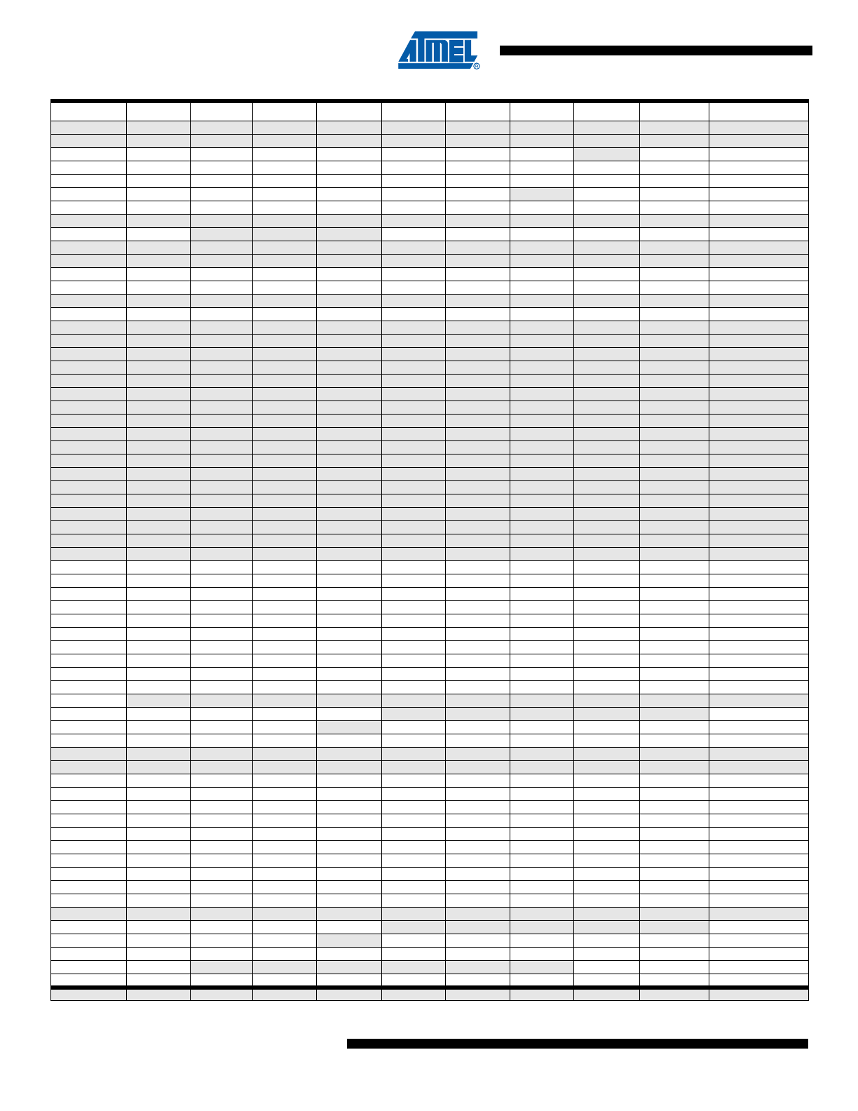
Address
Name
Bit 7
Bit 6
Bit 5
Bit 4
Bit 3
Bit 2
Bit 1
Bit 0
Page