

Features
•
High-performance, Low-power 32-bit Atmel
®
AVR
®
Microcontroller
– Compact Single-cycle RISC Instruction Set Including DSP Instructions
– Read-modify-write Instructions and Atomic Bit Manipulation
– Performance
• Up to 64DMIPS Running at 50MHz from Flash (1 Flash Wait State)
• Up to 36DMIPS Running at 25MHz from Flash (0 Flash Wait State)
– Memory Protection Unit (MPU)
• Secure Access Unit (SAU) providing User-defined Peripheral Protection
•
picoPower
®
Technology for Ultra-low Power Consumption
•
Multi-hierarchy Bus System
– High-performance Data Transfers on Separate Buses for Increased Performance
– 12 Peripheral DMA Channels Improve Speed for Peripheral Communication
•
Internal High-speed Flash
– 64Kbytes, 32Kbytes, and 16Kbytes Versions
– Single-cycle Access up to 25MHz
– FlashVault Technology Allows Pre-programmed Secure Library Support for End
User Applications
– Prefetch Buffer Optimizing Instruction Execution at Maximum Speed
– 100,000 Write Cycles, 15-year Data Retention Capability
– Flash Security Locks and User-defined Configuration Area
•
Internal High-speed SRAM, Single-cycle Access at Full Speed
– 16Kbytes (64Kbytes and 32Kbytes Flash), or 8Kbytes (16Kbytes Flash)
•
Interrupt Controller (INTC)
– Autovectored Low-latency Interrupt Service with Programmable Priority
•
External Interrupt Controller (EIC)
•
Peripheral Event System for Direct Peripheral to Peripheral Communication
•
System Functions
– Power and Clock Manager
– SleepWalking Power Saving Control
– Internal System RC Oscillator (RCSYS)
– 32KHz Oscillator
– Multipurpose Oscillator and Digital Frequency Locked Loop (DFLL)
•
Windowed Watchdog Timer (WDT)
•
Asynchronous Timer (AST) with Real-time Clock Capability
– Counter or Calendar Mode Supported
•
Frequency Meter (FREQM) for Accurate Measuring of Clock Frequency
•
Six 16-bit Timer/Counter (TC) Channels
– External Clock Inputs, PWM, Capture, and Various Counting Capabilities
•
36 PWM Channels (PWMA)
– 8-bit PWM with a Source Clock up to 150MHz
•
Four Universal Synchronous/Asynchronous Receiver/Transmitters (USART)
– Independent Baudrate Generator, Support for SPI
– Support for Hardware Handshaking
•
One Master/Slave Serial Peripheral Interfaces (SPI) with Chip Select Signals
– Up to 15 SPI Slaves can be Addressed
•
Two Master and Two Slave Two-wire Interface (TWI), 400kbit/s I
2
C-compatible
•
One 8-channel Analog-to-digital Converter (ADC) with up to 12 Bits Resolution
– Internal Temperature Sensor
32099IS–01/2012
32-bit Atmel
AVR
Microcontroller
AT32UC3L064
AT32UC3L032
AT32UC3L016
Summary

2
32099IS–01/2012
AT32UC3L016/32/64
•
Eight Analog Comparators (AC) with Optional Window Detection
•
Capacitive Touch (CAT) Module
– Hardware-assisted Atmel
®
AVR
®
QTouch
®
and Atmel
®
AVR
®
QMatrix Touch Acquisition
– Supports QTouch and QMatrix Capture from Capacitive Touch Sensors
•
QTouch Library Support
– Capacitive Touch Buttons, Sliders, and Wheels
– QTouch and QMatrix Acquisition
•
On-chip Non-intrusive Debug System
– Nexus Class 2+, Runtime Control, Non-intrusive Data and Program Trace
– aWire Single-pin Programming Trace and Debug Interface Muxed with Reset Pin
– NanoTrace Provides Trace Capabilities through JTAG or aWire Interface
•
48-pin TQFP/QFN/TLLGA (36 GPIO Pins)
•
Five High-drive I/O Pins
•
Single 1.62-3.6 V Power Supply

3
32099IS–01/2012
AT32UC3L016/32/64
1.
Description
The Atmel
®
AVR
®
AT32UC3L016/32/64 is a complete system-on-chip microcontroller based on
the AVR32 UC RISC processor running at frequencies up to 50MHz. AVR32 UC is a high-per-
formance 32-bit RISC microprocessor core, designed for cost-sensitive embedded applications,
with particular emphasis on low power consumption, high code density, and high performance.
The processor implements a Memory Protection Unit (MPU) and a fast and flexible interrupt con-
troller for supporting modern and real-time operating systems. The Secure Access Unit (SAU) is
used together with the MPU to provide the required security and integrity.
Higher computation capability is achieved using a rich set of DSP instructions.
The AT32UC3L016/32/64 embeds state-of-the-art picoPower technology for ultra-low power
consumption. Combined power control techniques are used to bring active current consumption
down to 165
µ
A/MHz, and leakage down to 9nA while still retaining a bank of backup registers.
The device allows a wide range of trade-offs between functionality and power consumption, giv-
ing the user the ability to reach the lowest possible power consumption with the feature set
required for the application.
The Peripheral Direct Memory Access (DMA) controller enables data transfers between periph-
erals and memories without processor involvement. The Peripheral DMA controller drastically
reduces processing overhead when transferring continuous and large data streams.
The AT32UC3L016/32/64 incorporates on-chip Flash and SRAM memories for secure and fast
access. The FlashVault technology allows secure libraries to be programmed into the device.
The secure libraries can be executed while the CPU is in Secure State, but not read by non-
secure software in the device. The device can thus be shipped to end customers, who will be
able to program their own code into the device to access the secure libraries, but without risk of
compromising the proprietary secure code.
The External Interrupt Controller (EIC) allows pins to be configured as external interrupts. Each
external interrupt has its own interrupt request and can be individually masked.
The Peripheral Event System allows peripherals to receive, react to, and send peripheral events
without CPU intervention. Asynchronous interrupts allow advanced peripheral operation in low
power sleep modes.
The Power Manager (PM) improves design flexibility and security. The Power Manager supports
SleepWalking functionality, by which a module can be selectively activated based on peripheral
events, even in sleep modes where the module clock is stopped. Power monitoring is supported
by on-chip Power-on Reset (POR), Brown-out Detector (BOD), and Supply Monitor (SM). The
device features several oscillators, such as Digital Frequency Locked Loop (DFLL), Oscillator 0
(OSC0), and system RC oscillator (RCSYS). Either of these oscillators can be used as source
for the system clock. The DFLL is a programmable internal oscillator from 40 to 150MHz. It can
be tuned to a high accuracy if an accurate refernce clock is running, e.g. the 32 KHz crystal
oscillator.
The Watchdog Timer (WDT) will reset the device unless it is periodically serviced by the soft-
ware. This allows the device to recover from a condition that has caused the system to be
unstable.
The Asynchronous Timer (AST) combined with the 32KHz crystal oscillator supports powerful
real-time clock capabilities, with a maximum timeout of up to 136 years. The AST can operate in
counter mode or calendar mode.

4
32099IS–01/2012
AT32UC3L016/32/64
The Frequency Meter (FREQM) allows accurate measuring of a clock frequency by comparing it
to a known reference clock.
The device includes six identical 16-bit Timer/Counter (TC) channels. Each channel can be inde-
pendently programmed to perform frequency measurement, event counting, interval
measurement, pulse generation, delay timing, and pulse width modulation.
The Pulse Width Modulation controller (PWMA) provides 8-bit PWM channels which can be syn-
chronized and controlled from a common timer. One PWM channel is available for each I/O pin
on the device, enabling applications that require multiple PWM outputs, such as LCD backlight
control. The PWM channels can operate independently, with duty cycles set independently from
each other, or in interlinked mode, with multiple channels changed at the same time.
The AT32UC3L016/32/64 also features many communication interfaces, like USART, SPI, and
TWI, for communication intensive applications. The USART supports different communication
modes, like SPI Mode and LIN Mode.
A general purpose 8-channel ADC is provided, as well as eight analog comparators (AC). The
ADC can operate in 10-bit mode at full speed or in enhanced mode at reduced speed, offering
up to 12-bit resolution. The ADC also provides an internal temperature sensor input channel.
The analog comparators can be paired to detect when the sensing voltage is within or outside
the defined reference window.
The Capacitive Touch (CAT) module senses touch on external capacitive touch sensors, using
the QTouch technology. Capacitive touch sensors use no external mechanical components,
unlike normal push buttons, and therefore demand less maintenance in the user application.
The CAT module allows up to 17 touch sensors, or up to 16 by 8 matrix sensors to be interfaced.
One touch sensor can be configured to operate autonomously without software interaction,
allowing wakeup from sleep modes when activated.
Atmel offers the QTouch library for embedding capacitive touch buttons, sliders, and wheels
functionality into AVR microcontrollers. The patented charge-transfer signal acquisition offers
robust sensing and includes fully debounced reporting of touch keys as well as Adjacent Key
Suppression
®
(AKS
®
) technology for unambiguous detection of key events. The easy-to-use
QTouch Suite toolchain allows you to explore, develop, and debug your own touch applications.
The AT32UC3L016/32/64 integrates a class 2+ Nexus 2.0 On-chip Debug (OCD) System, with
non-intrusive real-time trace and full-speed read/write memory access, in addition to basic run-
time control. The NanoTrace interface enables trace feature for aWire- or JTAG-based
debuggers. The single-pin aWire interface allows all features available through the JTAG inter-
face to be accessed through the RESET pin, allowing the JTAG pins to be used for GPIO or
peripherals.
5
32099IS–01/2012
AT32UC3L016/32/64
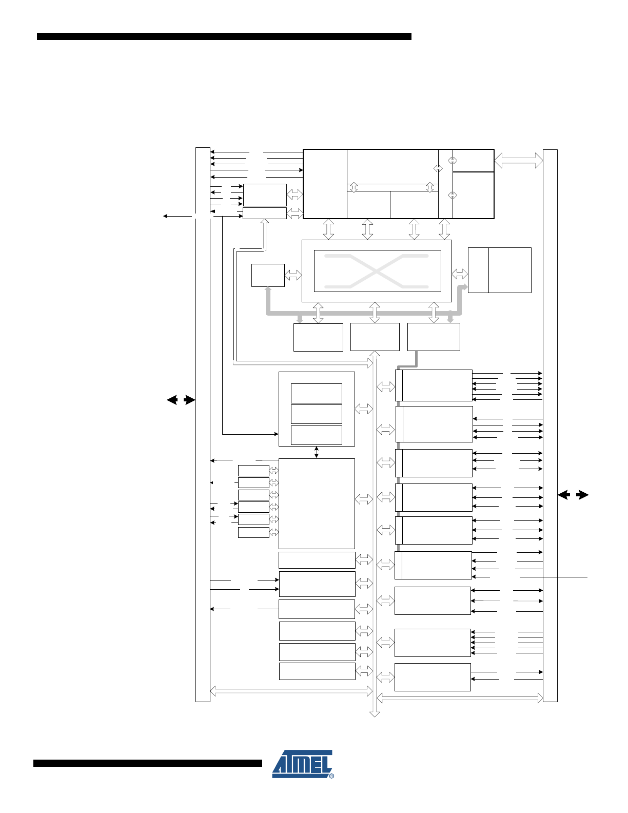
2.
Overview
2.1
Block Diagram
Figure 2-1.
Block Diagram
SYSTEM CONTROL
INTERFACE
INTERRUPT
CONTROLLER
ASYNCHRONOUS
TIMER
PERIPHERAL
DMA
CONTROLLER
HSB-PB
BRIDGE B
HSB-PB
BRIDGE A
S
M
M
M
S
S
M
EXTERNAL INTERRUPT
CONTROLLER
HIGH SPEED
BUS MATRIX
GEN
E
RA
LP
U
R
POSE
I/
Os
G
E
NERAL
PU
RP
O
SE I/O
s
PA
PB
EXTINT[5..1]
NMI
GCLK[4..0]
PA
PB
SPI
DM
A
MISO, MOSI
NPCS[3..0]
USART0
USART1
USART2
USART3
DM
A
RXD
TXD
CLK
RTS, CTS
WATCHDOG
TIMER
SCK
JTAG
INTERFACE
MCKO
MDO[5..0]
MSEO[1..0]
EVTI_N
TDO
TDI
TMS
CONFIGURATION REGISTERS BUS
64/32/16 KB
FLASH
S
FLAS
H
CON
T
ROL
LE
R
EVTO_N
AVR32UC CPU
NEXUS
CLASS 2+
OCD
INSTR
INTERFACE
DATA
INTERFACE
ME
MO
RY
I
N
T
E
R
F
A
C
E
LOCAL BUS
16/8 KB
SRAM
MEMORY PROTECTION UNIT
LOCAL BUS
INTERFACE
FREQUENCY METER
PWM CONTROLLER
PWMA[35..0]
TIMER/COUNTER 0
TIMER/COUNTER 1
A[2..0]
B[2..0]
TWI MASTER 0
TWI MASTER 1
DM
A
TWI SLAVE 0
TWI SLAVE 1
DM
A
8-CHANNEL ADC
INTERFACE
DM
A
AD[8..0]
ADVREFP
POWER MANAGER
RESET
CONTROLLER
SLEEP
CONTROLLER
CLOCK
CONTROLLER
XIN32
XOUT32
OSC32K
RCSYS
XIN0
XOUT0
OSC0
DFLL
TCK
aWire
RESET_N
CAPACITIVE TOUCH
MODULE
DM
A
CSB[16:0]
SMP
CSA[16:0]
SYNC
AC INTERFACE
ACREFN
ACAN[3..0]
ACBN[3..0]
ACBP[3..0]
ACAP[3..0]
TWCK
TWD
TWALM
TWCK
TWD
TWALM
RC32K
RC120M
GLUE LOGIC
CONTROLLER
IN[7..0]
OUT[1:0]
DATAOUT
SAU
S/M
VDIVEN
DIS
TRIGGER
ADP[1..0]
RC32OUT
CLK[2..0]

6
32099IS–01/2012
AT32UC3L016/32/64
2.2
Configuration Summary
Table 2-1.
Configuration Summary
Feature
AT32UC3L064
AT32UC3L032
AT32UC3L016
Flash
64KB
32KB
16KB
SRAM
16KB
16KB
8KB
GPIO
36
High-drive pins
5
External Interrupts
6
TWI
2
USART
4
Peripheral DMA Channels
12
Peripheral Event System
1
SPI
1
Asynchronous Timers
1
Timer/Counter Channels
6
PWM channels
36
Frequency Meter
1
Watchdog Timer
1
Power Manager
1
Secure Access Unit
1
Glue Logic Controller
1
Oscillators
Digital Frequency Locked Loop 40-150MHz (DFLL)
Crystal Oscillator 3-16MHz (OSC0)
Crystal Oscillator 32KHz (OSC32K)
RC Oscillator 120MHz (RC120M)
RC Oscillator 115kHz (RCSYS)
RC Oscillator 32kHz (RC32K)
ADC
8-channel 12-bit
Temperature Sensor
1
Analog Comparators
8
Capacitive Touch Module
1
JTAG
1
aWire
1
Max Frequency
50MHz
Packages
TQFP48/QFN48/TLLGA48
7
32099IS–01/2012
AT32UC3L016/32/64
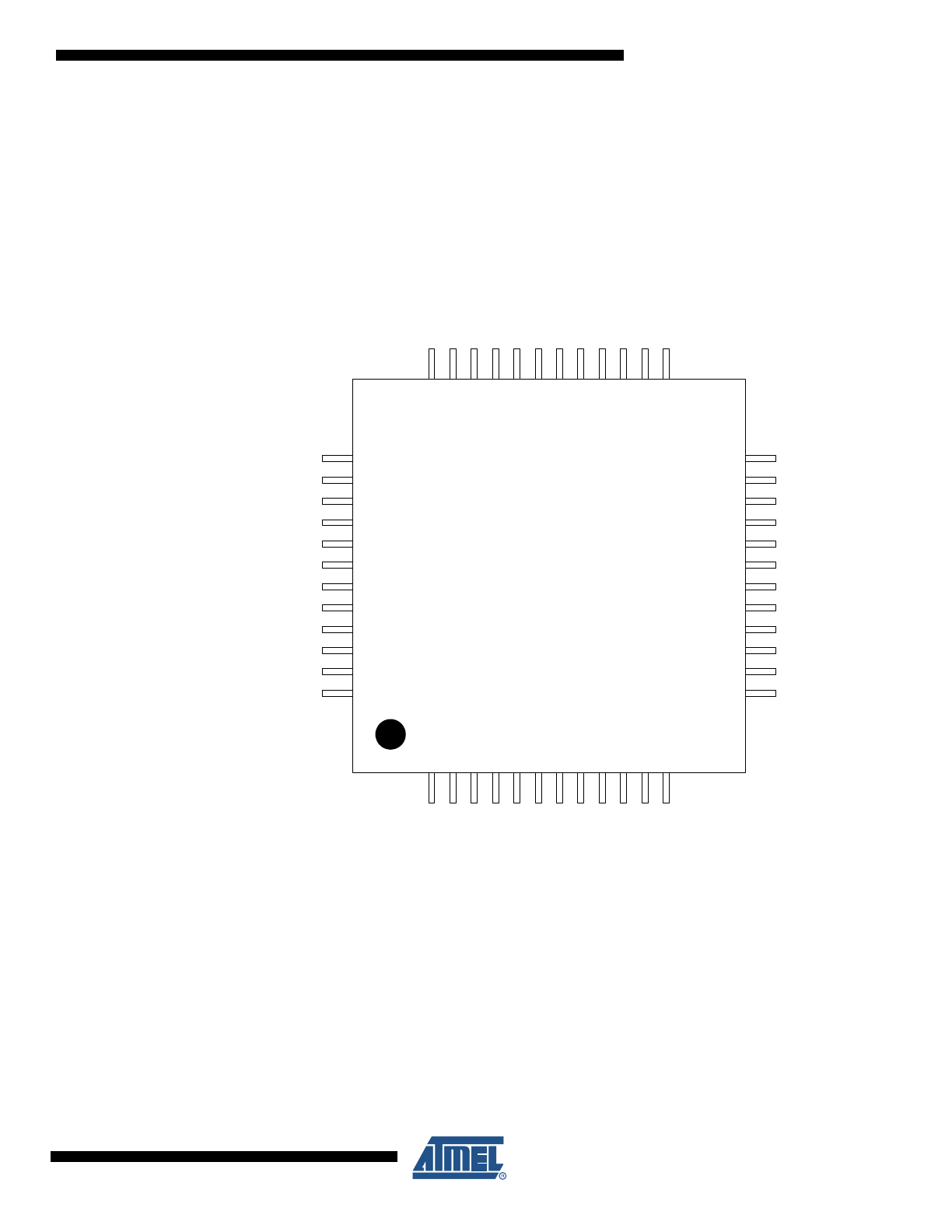
3.
Package and Pinout
3.1
Package
The device pins are multiplexed with peripheral functions as described in
Section 3.2
.
Figure 3-1.
TQFP48/QFN48 Pinout
GN
D
1
PA
09
2
PA
08
3
PA
03
4
PB
12
5
PB
00
6
PB
02
7
PB
03
8
PA
22
9
PA
06
10
PA
00
11
PA
05
12
PA02
13
PA01
14
PA07
15
PB01
16
VDDIN
17
VDDCORE
18
GND
19
PB05
20
PB04
21
RESET_N
22
PB10
23
PA21
24
PA
14
36
VD
D
A
NA
35
AD
VR
E
F
P
34
GN
DA
NA
33
PB
08
32
PB
07
31
PB
06
30
PB
09
29
PA
04
28
PA
11
27
PA
13
26
PA
20
25
PA15
37
PA16
38
PA17
39
PA19
40
PA18
41
VDDIO
42
GND
43
PB11
44
GND
45
PA10
46
PA12
47
VDDIO
48
8
32099IS–01/2012
AT32UC3L016/32/64
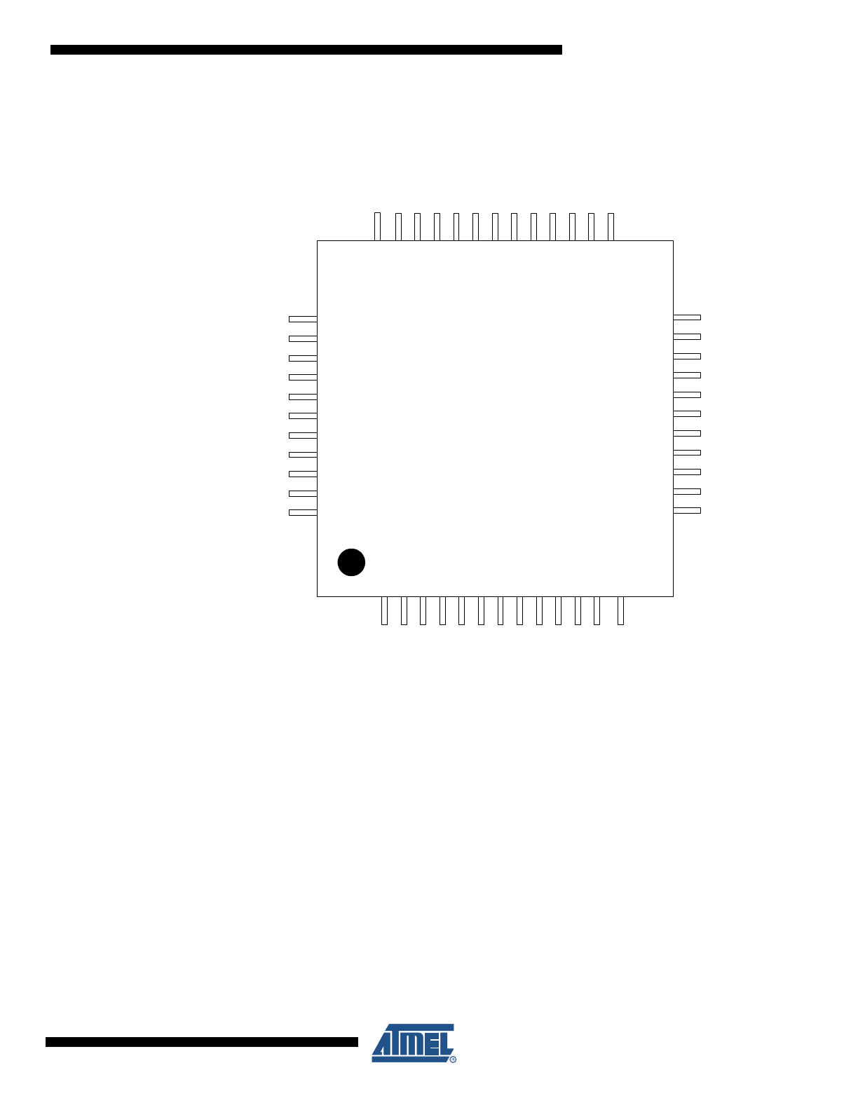
Figure 3-2.
TLLGA48 Pinout
GND
1
PA09
2
PA08
3
PA03
4
PB12
5
PB00
6
PB02
7
PB03
8
PA22
9
PA06
10
PA00
11
PA05
12
PA
02
13
PA01
14
PA07
15
PB01
16
VDDIN
17
VDDCORE
18
GND
19
PB05
20
PB04
21
RESET_N
22
PB10
23
PA21
24
PA14
36
V
DDA
N
A
35
AD
VR
EFP
34
GN
DA
NA
33
PB08
32
PB07
31
PB06
30
PB09
29
PA04
28
PA11
27
PA13
26
PA20
25
PA
15
37
PA16
38
PA17
39
PA19
40
PA18
41
VDDIO
42
GND
43
PB11
44
GND
45
PA10
46
PA12
47
VDDIO
48

9
32099IS–01/2012
AT32UC3L016/32/64
3.2
Peripheral Multiplexing on I/O lines
3.2.1
Multiplexed signals
Each GPIO line can be assigned to one of the peripheral functions.The following table describes
the peripheral signals multiplexed to the GPIO lines.
Table 3-1.
GPIO Controller Function Multiplexing
48-
pin
PIN
G
P
I
O
Supply
Pin
Type
GPIO Function
A
B
C
D
E
F
G
H
11
PA00
0
VDDIO
Normal
I/O
USART0
TXD
USART1
RTS
SPI
NPCS[2]
PWMA
PWMA[0]
SCIF
GCLK[0]
CAT
CSA[2]
14
PA01
1
VDDIO
Normal
I/O
USART0
RXD
USART1
CTS
SPI
NPCS[3]
USART1
CLK
PWMA
PWMA[1]
ACIFB
ACAP[0]
TWIMS0
TWALM
CAT
CSA[1]
13
PA02
2
VDDIO
High-
drive I/O
USART0
RTS
ADCIFB
TRIGGER
USART2
TXD
TC0
A0
PWMA
PWMA[2]
ACIFB
ACBP[0]
USART0
CLK
CAT
CSA[3]
4
PA03
3
VDDIO
Normal
I/O
USART0
CTS
SPI
NPCS[1]
USART2
TXD
TC0
B0
PWMA
PWMA[3]
ACIFB
ACBN[3]
USART0
CLK
CAT
CSB[3]
28
PA04
4
VDDIO
Normal
I/O
SPI
MISO
TWIMS0
TWCK
USART1
RXD
TC0
B1
PWMA
PWMA[4]
ACIFB
ACBP[1]
CAT
CSA[7]
12
PA05
5
VDDIO
Normal
I/O (TWI)
SPI
MOSI
TWIMS1
TWCK
USART1
TXD
TC0
A1
PWMA
PWMA[5]
ACIFB
ACBN[0]
TWIMS0
TWD
CAT
CSB[7]
10
PA06
6
VDDIO
High-
drive I/O,
5V
tolerant
SPI
SCK
USART2
TXD
USART1
CLK
TC0
B0
PWMA
PWMA[6]
SCIF
GCLK[1]
CAT
CSB[1]
15
PA07
7
VDDIO
Normal
I/O (TWI)
SPI
NPCS[0]
USART2
RXD
TWIMS1
TWALM
TWIMS0
TWCK
PWMA
PWMA[7]
ACIFB
ACAN[0]
EIC
EXTINT[0]
CAT
CSB[2]
3
PA08
8
VDDIO
High-
drive I/O
USART1
TXD
SPI
NPCS[2]
TC0
A2
ADCIFB
ADP[0]
PWMA
PWMA[8]
CAT
CSA[4]
2
PA09
9
VDDIO
High-
drive I/O
USART1
RXD
SPI
NPCS[3]
TC0
B2
ADCIFB
ADP[1]
PWMA
PWMA[9]
SCIF
GCLK[2]
EIC
EXTINT[1]
CAT
CSB[4]
46
PA10
10
VDDIO
Normal
I/O
TWIMS0
TWD
TC0
A0
PWMA
PWMA[10]
ACIFB
ACAP[1]
SCIF
GCLK[2]
CAT
CSA[5]
27
PA11
11
VDDIN
Normal
I/O
PWMA
PWMA[11]
47
PA12
12
VDDIO
Normal
I/O
USART2
CLK
TC0
CLK1
CAT
SMP
PWMA
PWMA[12]
ACIFB
ACAN[1]
SCIF
GCLK[3]
CAT
CSB[5]
26
PA13
13
VDDIN
Normal
I/O
GLOC
OUT[0]
GLOC
IN[7]
TC0
A0
SCIF
GCLK[2]
PWMA
PWMA[13]
CAT
SMP
EIC
EXTINT[2]
CAT
CSA[0]
36
PA14
14
VDDIO
Normal
I/O
ADCIFB
AD[0]
TC0
CLK2
USART2
RTS
CAT
SMP
PWMA
PWMA[14]
SCIF
GCLK[4]
CAT
CSA[6]
37
PA15
15
VDDIO
Normal
I/O
ADCIFB
AD[1]
TC0
CLK1
GLOC
IN[6]
PWMA
PWMA[15]
CAT
SYNC
EIC
EXTINT[3]
CAT
CSB[6]
38
PA16
16
VDDIO
Normal
I/O
ADCIFB
AD[2]
TC0
CLK0
GLOC
IN[5]
PWMA
PWMA[16]
ACIFB
ACREFN
EIC
EXTINT[4]
CAT
CSA[8]
39
PA17
17
VDDIO
Normal
I/O (TWI)
TC0
A1
USART2
CTS
TWIMS1
TWD
PWMA
PWMA[17]
CAT
SMP
CAT
DIS
CAT
CSB[8]
41
PA18
18
VDDIO
Normal
I/O
ADCIFB
AD[4]
TC0
B1
GLOC
IN[4]
PWMA
PWMA[18]
CAT
SYNC
EIC
EXTINT[5]
CAT
CSB[0]

10
32099IS–01/2012
AT32UC3L016/32/64
See
Section 3.3
for a description of the various peripheral signals.
Refer to
”Electrical Characteristics” on page 41
for a description of the electrical properties of the
pin types used.
3.2.1.1
TWI, 5V Tolerant, and SMBUS Pins
Some Normal I/O pins offer TWI, 5V Tolerant, and SMBUS features. These features are only
available when either of the TWI functions or the PWMAOD function in the PWMA are selected
for these pins.
40
PA19
19
VDDIO
Normal
I/O
ADCIFB
AD[5]
TC0
A2
TWIMS1
TWALM
PWMA
PWMA[19]
CAT
SYNC
CAT
CSA[10]
25
PA20
20
VDDIN
Normal
I/O
USART2
TXD
TC0
A1
GLOC
IN[3]
PWMA
PWMA[20]
SCIF
RC32OUT
CAT
CSA[12]
24
PA21
21
VDDIN
Normal
I/O (TWI,
5V
tolerant
SMBus)
USART2
RXD
TWIMS0
TWD
TC0
B1
ADCIFB
TRIGGER
PWMA
PWMA[21]
PWMA
PWMAOD[21]
SCIF
GCLK[0]
CAT
SMP
9
PA22
22
VDDIO
Normal
I/O
USART0
CTS
USART2
CLK
TC0
B2
CAT
SMP
PWMA
PWMA[22]
ACIFB
ACBN[2]
CAT
CSB[10]
6
PB00
32
VDDIO
Normal
I/O
USART3
TXD
ADCIFB
ADP[0]
SPI
NPCS[0]
TC0
A1
PWMA
PWMA[23]
ACIFB
ACAP[2]
TC1
A0
CAT
CSA[9]
16
PB01
33
VDDIO
High-
drive I/O
USART3
RXD
ADCIFB
ADP[1]
SPI
SCK
TC0
B1
PWMA
PWMA[24]
TC1
A1
CAT
CSB[9]
7
PB02
34
VDDIO
Normal
I/O
USART3
RTS
USART3
CLK
SPI
MISO
TC0
A2
PWMA
PWMA[25]
ACIFB
ACAN[2]
SCIF
GCLK[1]
CAT
CSB[11]
8
PB03
35
VDDIO
Normal
I/O
USART3
CTS
USART3
CLK
SPI
MOSI
TC0
B2
PWMA
PWMA[26]
ACIFB
ACBP[2]
TC1
A2
CAT
CSA[11]
21
PB04
36
VDDIN
Normal
I/O (TWI,
5V
tolerant
SMBus)
TC1
A0
USART1
RTS
USART1
CLK
TWIMS0
TWALM
PWMA
PWMA[27]
PWMA
PWMAOD[27]
TWIMS1
TWCK
CAT
CSA[14]
20
PB05
37
VDDIN
Normal
I/O (TWI,
5V
tolerant
SMBus)
TC1
B0
USART1
CTS
USART1
CLK
TWIMS0
TWCK
PWMA
PWMA[28]
PWMA
PWMAOD[28]
SCIF
GCLK[3]
CAT
CSB[14]
30
PB06
38
VDDIO
Normal
I/O
TC1
A1
USART3
TXD
ADCIFB
AD[6]
GLOC
IN[2]
PWMA
PWMA[29]
ACIFB
ACAN[3]
EIC
EXTINT[0]
CAT
CSB[13]
31
PB07
39
VDDIO
Normal
I/O
TC1
B1
USART3
RXD
ADCIFB
AD[7]
GLOC
IN[1]
PWMA
PWMA[30]
ACIFB
ACAP[3]
EIC
EXTINT[1]
CAT
CSA[13]
32
PB08
40
VDDIO
Normal
I/O
TC1
A2
USART3
RTS
ADCIFB
AD[8]
GLOC
IN[0]
PWMA
PWMA[31]
CAT
SYNC
EIC
EXTINT[2]
CAT
CSB[12]
29
PB09
41
VDDIO
Normal
I/O
TC1
B2
USART3
CTS
USART3
CLK
PWMA
PWMA[32]
ACIFB
ACBN[1]
EIC
EXTINT[3]
CAT
CSB[15]
23
PB10
42
VDDIN
Normal
I/O
TC1
CLK0
USART1
TXD
USART3
CLK
GLOC
OUT[1]
PWMA
PWMA[33]
EIC
EXTINT[4]
CAT
CSB[16]
44
PB11
43
VDDIO
Normal
I/O
TC1
CLK1
USART1
RXD
ADCIFB
TRIGGER
PWMA
PWMA[34]
CAT
VDIVEN
EIC
EXTINT[5]
CAT
CSA[16]
5
PB12
44
VDDIO
Normal
I/O
TC1
CLK2
TWIMS1
TWALM
CAT
SYNC
PWMA
PWMA[35]
ACIFB
ACBP[3]
SCIF
GCLK[4]
CAT
CSA[15]
Table 3-1.
GPIO Controller Function Multiplexing