

NOTE: This is a summary document.
The complete document is available on
the Atmel website at www.atmel.com.
Features
•
High Performance, Low Power 32-bit AVR
®
Microcontroller
– Compact Single-cycle RISC Instruction Set Including DSP Instruction Set
– Built-in Floating-Point Processing Unit (FPU)
– Read-Modify-Write Instructions and Atomic Bit Manipulation
– Performing 1.49 DMIPS / MHz
• Up to 91 DMIPS Running at 66 MHz from Flash (1 Wait-State)
• Up to 49 DMIPS Running at 33 MHz from Flash (0 Wait-State)
– Memory Protection Unit
•
Multi-hierarchy Bus System
– High-Performance Data Transfers on Separate Buses for Increased Performance
– 16 Peripheral DMA Channels Improves Speed for Peripheral Communication
•
Internal High-Speed Flash
– 512 Kbytes, 256 Kbytes, 128 Kbytes, 64 Kbytes Versions
– Single Cycle Access up to 33 MHz
– FlashVault
™
Technology Allows Pre-programmed Secure Library Support for End
User Applications
– Prefetch Buffer Optimizing Instruction Execution at Maximum Speed
– 100,000 Write Cycles, 15-year Data Retention Capability
– Flash Security Locks and User Defined Configuration Area
•
Internal High-Speed SRAM, Single-Cycle Access at Full Speed
– 64 Kbytes (512 KB and 256 KB Flash), 32 Kbytes (128 KB Flash), 16 Kbytes (64 KB
Flash)
– 4 Kbytes on the Multi-Layer Bus System (HSB RAM)
•
External Memory Interface on AT32UC3C0 Derivatives
– SDRAM / SRAM Compatible Memory Bus (16-bit Data and 24-bit Address Buses)
•
Interrupt Controller
– Autovectored Low Latency Interrupt Service with Programmable Priority
•
System Functions
– Power and Clock Manager
– Internal 115KHz (RCSYS) and 8MHz/1MHz (RC8M) RC Oscillators
– One 32 KHz and Two Multipurpose Oscillators
– Clock Failure detection
– Two Phase-Lock-Loop (PLL) allowing Independent CPU Frequency from USB or
CAN Frequency
•
Windowed Watchdog Timer (WDT)
•
Asynchronous Timer (AST) with Real-Time Clock Capability
– Counter or Calendar Mode Supported
•
Frequency Meter (FREQM) for Accurate Measuring of Clock Frequency
•
Ethernet MAC 10/100 Mbps interface
– 802.3 Ethernet Media Access Controller
– Supports Media Independent Interface (MII) and Reduced MII (RMII)
•
Universal Serial Bus (USB)
– Device 2.0 and Embedded Host Low Speed and Full Speed
– Flexible End-Point Configuration and Management with Dedicated DMA Channels
– On-chip Transceivers Including Pull-Ups
•
One 2-channel Controller Area Network (CAN)
– CAN2A and CAN2B protocol compliant, with high-level mailbox system
– Two independent channels, 16 Message Objects per Channel
32117DS–AVR–01/12
32-bit AVR
®
Microcontroller
AT32UC3C0512C
AT32UC3C0256C
AT32UC3C0128C
AT32UC3C064C
AT32UC3C1512C
AT32UC3C1256C
AT32UC3C1128C
AT32UC3C164C
AT32UC3C2512C
AT32UC3C2256C
AT32UC3C2128C
AT32UC3C264C
Summary

2
32117DS–AVR-01/12
AT32UC3C
•
One 4-Channel 20-bit Pulse Width Modulation Controller (PWM)
– Complementary outputs, with Dead Time Insertion
– Output Override and Fault Protection
•
Two Quadrature Decoders
•
One 16-channel 12-bit Pipelined Analog-To-Digital Converter (ADC)
– Dual Sample and Hold Capability Allowing 2 Synchronous Conversions
– Single-Ended and Differential Channels, Window Function
•
Two 12-bit Digital-To-Analog Converters (DAC), with Dual Output Sample System
•
Four Analog Comparators
•
Six 16-bit Timer/Counter (TC) Channels
– External Clock Inputs, PWM, Capture and Various Counting Capabilities
•
One Peripheral Event Controller
– Trigger Actions in Peripherals Depending on Events Generated from Peripherals or from Input Pins
– Deterministic Trigger
– 34 Events and 22 Event Actions
•
Five Universal Synchronous/Asynchronous Receiver/Transmitters (USART)
– Independent Baudrate Generator, Support for SPI, LIN, IrDA and ISO7816 interfaces
– Support for Hardware Handshaking, RS485 Interfaces and Modem Line
•
Two Master/Slave Serial Peripheral Interfaces (SPI) with Chip Select Signals
•
One Inter-IC Sound (I2S) Controller
– Compliant with I2S Bus Specification
– Time Division Multiplexed mode
•
Three Master and Three Slave Two-Wire Interfaces (TWI), 400kbit/s I
2
C-compatible
•
QTouch
®
Library Support
– Capacitive Touch Buttons, Sliders, and Wheels
– QTouch
®
and QMatrix
®
Acquisition
•
On-Chip Non-intrusive Debug System
– Nexus Class 2+, Runtime Control, Non-Intrusive Data and Program Trace
– aWire
™
single-pin programming trace and debug interface muxed with reset pin
– NanoTrace
™
provides trace capabilities through JTAG or aWire interface
•
3 package options
– 64-pin QFN/TQFP (45 GPIO pins)
– 100-pin TQFP (81 GPIO pins)
– 144-pin LQFP (123 GPIO pins)
•
Two operating voltage ranges:
– Single 5V Power Supply
– Single 3.3V Power Supply

3
32117DS–AVR-01/12
AT32UC3C
1.
Description
The AT32UC3C is a complete System-On-Chip microcontroller based on the AVR32UC RISC
processor running at frequencies up to 66 MHz. AVR32UC is a high-performance 32-bit RISC
microprocessor core, designed for cost-sensitive embedded applications, with particular empha-
sis on low power consumption, high code density and high performance.
The processor implements a Memory Protection Unit (MPU) and a fast and flexible interrupt con-
troller for supporting modern operating systems and real-time operating systems. Using the
Secure Access Unit (SAU) together with the MPU provides the required security and integrity.
Higher computation capabilities are achievable either using a rich set of DSP instructions or
using the floating-point instructions.
The AT32UC3C incorporates on-chip Flash and SRAM memories for secure and fast access.
For applications requiring additional memory, an external memory interface is provided on
AT32UC3C0 derivatives.
The Memory Direct Memory Access controller (MDMA) enables transfers of block of data from
memories to memories without processor involvement.
The Peripheral Direct Memory Access (PDCA) controller enables data transfers between periph-
erals and memories without processor involvement. The PDCA drastically reduces processing
overhead when transferring continuous and large data streams.
The AT32UC3C incorporates on-chip Flash and SRAM memories for secure and fast access.
The FlashVault technology allows secure libraries to be programmed into the device. The secure
libraries can be executed while the CPU is in Secure State, but not read by non-secure software
in the device. The device can thus be shipped to end custumers, who are able to program their
own code into the device, accessing the secure libraries, without any risk of compromising the
proprietary secure code.
The Power Manager improves design flexibility and security. Power monitoring is supported by
on-chip Power-On Reset (POR), Brown-Out Detectors (BOD18, BOD33, BOD50). The CPU
runs from the on-chip RC oscillators, the PLLs, or the Multipurpose Oscillators. The Asynchro-
nous Timer (AST) combined with the 32 KHz oscillator keeps track of the time. The AST can
operate in counter or calendar mode.
The device includes six identical 16-bit Timer/Counter (TC) channels. Each channel can be inde-
pendently programmed to perform frequency measurement, event counting, interval
measurement, pulse generation, delay timing, and pulse width modulation.
The PWM module provides four channels with many configuration options including polarity,
edge alignment and waveform non overlap control. The PWM channels can operate indepen-
dently, with duty cycles set independently from each other, or in interlinked mode, with multiple
channels updated at the same time. It also includes safety feature with fault inputs and the ability
to lock the PWM configuration registers and the PWM pin assignment.
The AT32UC3C also features many communication interfaces for communication intensive
applications. In addition to standard serial interfaces like UART, SPI or TWI, other interfaces like
flexible CAN, USB and Ethernet MAC are available. The USART supports different communica-
tion modes, like SPI mode and LIN mode.
The Inter-IC Sound Controller (I2SC) provides a 5-bit wide, bidirectional, synchronous, digital
audio link with off-chip audio devices. The controller is compliant with the I2S bus specification.

4
32117DS–AVR-01/12
AT32UC3C
The Full-Speed USB 2.0 Device interface supports several USB Classes at the same time
thanks to the rich End-Point configuration. The On-The-GO (OTG) Host interface allows device
like a USB Flash disk or a USB printer to be directly connected to the processor.
The media-independent interface (MII) and reduced MII (RMII) 10/100 Ethernet MAC module
provides on-chip solutions for network-connected devices.
The Peripheral Event Controller (PEVC) allows to redirect events from one peripheral or from
input pins to another peripheral. It can then trigger, in a deterministic time, an action inside a
peripheral without the need of CPU. For instance a PWM waveform can directly trigger an ADC
capture, hence avoiding delays due to software interrupt processing.
The AT32UC3C features analog functions like ADC, DAC, Analog comparators. The ADC inter-
face is built around a 12-bit pipelined ADC core and is able to control two independent 8-channel
or one 16-channel. The ADC block is able to measure two different voltages sampled at the
same time. The analog comparators can be paired to detect when the sensing voltage is within
or outside the defined reference window.
Atmel offers the QTouch library for embedding capacitive touch buttons, sliders, and wheels
functionality into AVR microcontrollers. The patented charge-transfer signal acquisition offers
robust sensing and included fully debounced reporting of touch keys and includes Adjacent Key
Suppression
®
(AKS
®
) technology for unambiguous detection of key events. The easy-to-use
QTouch Suite toolchain allows you to explore, develop, and debug your own touch applications.
AT32UC3C integrates a class 2+ Nexus 2.0 On-Chip Debug (OCD) System, with non-intrusive
real-time trace, full-speed read/write memory access in addition to basic runtime control. The
Nanotrace interface enables trace feature for aWire- or JTAG-based debuggers. The single-pin
aWire interface allows all features available through the JTAG interface to be accessed through
the RESET pin, allowing the JTAG pins to be used for GPIO or peripherals.
5
32117DS–AVR-01/12
AT32UC3C
2.
Overview
2.1
Block diagram
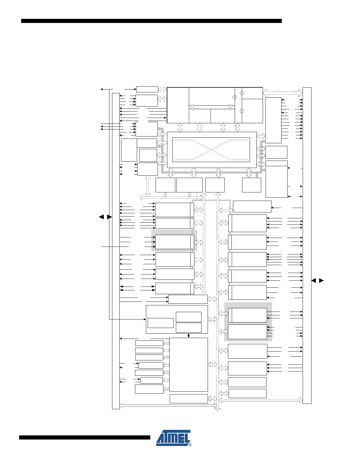
Figure 2-1.
Block diagram
supplied by VDDANA
supplied by VDDANA
PERIPHERAL
DMA
CONTROLLER
HSB-PB
BRIDGE B
HSB-PB
BRIDGE A
GENERAL
PURP
OS
E
IO
s
G
E
N
E
RA
L P
U
RP
O
S
E
IO
s
PA
PB
PC
PD
PA
PB
PC
PD
USB
INTERFACE
ID
VBOF
VBUS
D-
D+
CANIF
32 KHz OSC
RCSYS
OSC0 / OSC1
PLL0 / PLL1
JTAG
INTERFACE
MCKO
MDO[5..0]
MSEO[1..0]
EVTI_N
EVTO_N
TDI
RXLINE[0]
PB
PB
HSB
HSB
TXLINE[0]
RXLINE[1]
TXCAN[1]
PERIPHERAL EVENT
CONTROLLER
PAD_EVT
M
M
M
S
S
M
HIGH SPEED
BUS MATRIX
AVR32UC CPU
NEXUS
CLASS 2+
OCD
INSTR
INTERFACE
DATA
INTERFACE
ME
MOR
Y
IN
T
E
R
F
A
C
E
64/32/16
KB SRAM
MEMORY PROTECTION UNIT
LOCAL BUS
INTERFACE
M
4 KB
HSB
RAM
S
S
EXTERNAL BU
S
INTE
R
FA
C
E
(S
D
R
AM &
STATIC
MEMORY
C
O
NTROLLER)
CAS
RAS
SDA10
SDCK
SDCKE
SDWE
NCS[3..0]
NRD
NWAIT
NWE0
DATA[15..0]
ADDR[23..0]
NWE1
Memory
DMA
HSB-PB
BRIDGE C
PB
HSB
S
M
S
M
CONFIGURATION REGISTERS BUS
PBB
SERIAL
PERIPHERAL
INTERFACE 1
DM
A
MISO, MOSI
NPCS[3..0]
SCK
USART0
USART2
USART3
DM
A
RXD
TXD
CLK
RTS, CTS
TWCK
TWD
TWO-WIRE
INTERFACE 0/1
DM
A
PULSE WIDTH
MODULATION
CONTROLLER
DM
A
DIGITAL TO
ANALOG
CONVERTER 0/1
DM
A
DAC0A/B
ANALOG
COMPARATOR
0A/0B/1A/1B
AC0AP/N AC0BP/N
AC1AP/N AC1BP/N
DAC1A/B
I2S INTERFACE
DM
A
TIMER/COUNTER 1
A[2..0]
B[2..0]
CLK[2..0]
QUADRATURE
DECODER
0/1
QEPA
QEPB
QEPI
XIN32
XOUT32
XIN[1:0]
XOUT[1:0]
TIMER/COUNTER 0
CLK[2..0]
A[2..0]
B[2..0]
ANALOG TO
DIGITAL
CONVERTER 0/1
DM
A
ADCIN[15..0]
ADCVREFP/N
USART1
DM
A
RXD
TXD
CLK
RTS, CTS
DSR, DTR, DCD, RI
PB
C
PBA
SERIAL
PERIPHERAL
INTERFACE 0
DM
A
SCK
MISO, MOSI
NPCS[3..0]
M
R
W
PWML[3..0]
PWMH[3..0]
ADCREF0/1
aWire
RESET_N
ASYNCHRONOUS
TIMER
WATCHDOG
TIMER
FREQUENCY METER
POWER MANAGER
RESET
CONTROLLER
SLEEP
CONTROLLER
CLOCK
CONTROLLER
SYSTEM CONTROL
INTERFACE
GCLK[1..0]
BODs (1.8V,
3.3V, 5V)
RC8M
AC0AOUT/AC0BOUT
AC1AOUT/AC1BOUT
External Interrupt
Controller
EXTINT[8:1]
NMI
TWO-WIRE
INTERFACE 2
DM
A
TWD
TWCK
ETHERNET
MAC
DMA
S
COL,
CRS,
RXD[3..0],
RX_CLK,
RX_DV,
RX_ER,
TX_CLK
MDC,
TXD[3..0],
TX_EN,
TX_ER,
SPEED
MDIO
M
512/
256/
128/64
KB
Flash
Flash
Controller
BCLK
IWS
ISDO
MCLK
LOCAL BUS
DACREF
ISDI
TMS
TCK
TDO
RC120M
EXT_FAULTS[1:0]
TWALM
USART4
DM
A
RXD
TXD
CLK
RTS, CTS
6
32117DS–AVR-01/12
AT32UC3C
2.2
Configuration Summary
Table 2-1.
Configuration Summary
Feature
AT32UC3C0512C/
AT32UC3C0256C/
AT32UC3C0128C/
AT32UC3C064C
AT32UC3C1512C/
AT32UC3C1256C/
AT32UC3C1128C/
AT32UC3C164C
AT32UC3C2512C/
AT32UC3C2256C/
AT32UC3C2128C/
AT32UC3C264C
Flash
512/256/128/64 KB
512/256/128/64 KB
512/256/128/64 KB
SRAM
64/64/32/16KB
64/64/32/16KB
64/64/32/16KB
HSB RAM
4 KB
EBI
1
0
0
GPIO
123
81
45
External Interrupts
8
8
8
TWI
3
3
2
USART
5
5
4
Peripheral DMA Channels
16
16
16
Peripheral Event System
1
1
1
SPI
2
2
1
CAN channels
2
2
2
USB
1
1
1
Ethernet MAC 10/100
1
RMII/MII
1
RMII/MII
1
RMII only
I2S
1
1
1
Asynchronous Timers
1
1
1
Timer/Counter Channels
6
6
3
PWM channels
4x2
QDEC
2
2
1
Frequency Meter
1
Watchdog Timer
1
Power Manager
1
Oscillators
PLL 80-240 MHz (PLL0/PLL1)
Crystal Oscillator 0.4-20 MHz (OSC0)
Crystal Oscillator 32 KHz (OSC32K)
RC Oscillator 115 kHz (RCSYS)
RC Oscillator 8 MHz (RC8M)
RC Oscillator 120 MHz (RC120M)
0.4-20 MHz (OSC1)
-
12-bit ADC
number of channels
1
16
1
16
1
11
12-bit DAC
number of channels
1
4
1
4
1
2
7
32117DS–AVR-01/12
AT32UC3C
Analog Comparators
4
4
2
JTAG
1
aWire
1
Max Frequency
66 MHz
Package
LQFP144
TQFP100
TQFP64/QFN64
Table 2-1.
Configuration Summary
Feature
AT32UC3C0512C/
AT32UC3C0256C/
AT32UC3C0128C/
AT32UC3C064C
AT32UC3C1512C/
AT32UC3C1256C/
AT32UC3C1128C/
AT32UC3C164C
AT32UC3C2512C/
AT32UC3C2256C/
AT32UC3C2128C/
AT32UC3C264C
8
32117DS–AVR-01/12
AT32UC3C
3.
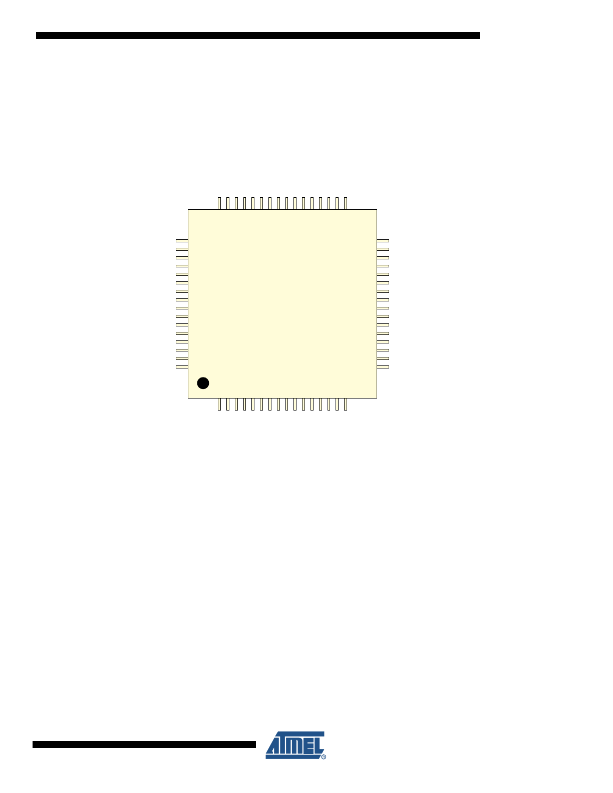
Package and Pinout
3.1
Package
The device pins are multiplexed with peripheral functions as described in
Table 3-1 on page 11
.
Figure 3-1.
QFN64/TQFP64 Pinout
Note:
on QFN packages, the exposed pad is unconnected.
PA00
1
PA01
2
PA02
3
PA03
4
VDDIO1
5
GNDIO1
6
PA04
7
PA05
8
PA06
9
PA07
10
PA08
11
PA09
12
PA16
13
ADCVREFP
14
ADCVREFN
15
PA19
16
GNDANA
17
VDDANA
18
PA20
19
PA21
20
PA22
21
PA23
22
VBUS
23
DM
24
DP
25
GNDPLL
26
VDDIN_5
27
VDDIN_33
28
VDDCORE
29
GNDCORE
30
PB30
31
PB31
32
PD01
48
PD00
47
PC22
46
PC21
45
PC20
44
PC19
43
PC18
42
PC17
41
PC16
40
PC15
39
PC05
38
PC04
37
GNDIO2
36
VDDIO2
35
PC03
34
PC02
33
PD02
49
PD03
50
VDDIO3
51
GNDIO3
52
PD11
53
PD12
54
PD13
55
PD14
56
PD21
57
PD27
58
PD28
59
PD29
60
PD30
61
PB00
62
PB01
63
RESET_N
64
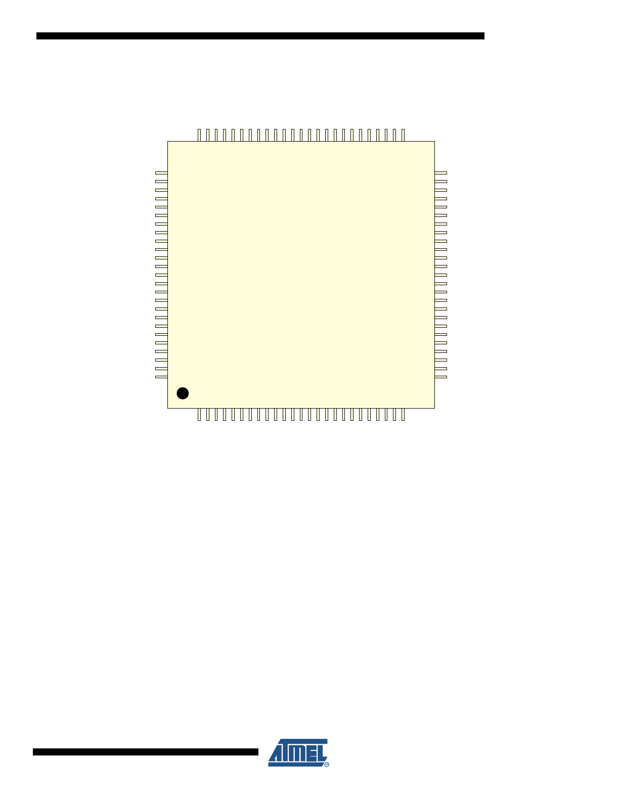
9
32117DS–AVR-01/12
AT32UC3C
Figure 3-2.
TQFP100 Pinout
PA00
1
PA01
2
PA02
3
PA03
4
VDDIO1
5
GNDIO1
6
PB04
7
PB05
8
PB06
9
PA04
10
PA05
11
PA06
12
PA07
13
PA08
14
PA09
15
PA10
16
PA
11
17
PA12
18
PA13
19
PA14
20
PA15
21
PA16
22
ADCVREFP
23
ADCVREFN
24
PA19
25
GNDANA
26
VDDANA
27
PA20
28
PA21
29
PA22
30
PA23
31
PA24
32
PA25
33
VBUS
34
DM
35
DP
36
GNDPLL
37
VDDIN_5
38
VDDIN_33
39
VDDCORE
40
GNDCORE
41
PB19
42
PB20
43
PB21
44
PB22
45
PB23
46
PB30
47
PB31
48
PC00
49
PC01
50
PD01
75
PD00
74
PC31
73
PC24
72
PC23
71
PC22
70
PC21
69
PC20
68
PC19
67
PC18
66
PC17
65
PC16
64
PC15
63
PC14
62
PC13
61
PC12
60
PC1
1
59
PC07
58
PC06
57
PC05
56
PC04
55
GNDIO2
54
VDDIO2
53
PC03
52
PC02
51
PD02
76
PD03
77
PD07
78
PD08
79
PD09
80
PD10
81
VDDIO3
82
GNDIO3
83
PD11
84
PD12
85
PD13
86
PD14
87
PD21
88
PD22
89
PD23
90
PD24
91
PD27
92
PD28
93
PD29
94
PD30
95
PB00
96
PB01
97
RESET_N
98
PB02
99
PB03
100
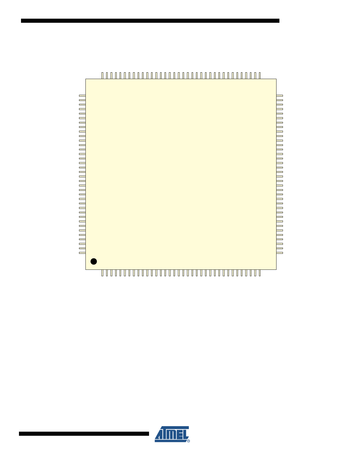
10
32117DS–AVR-01/12
AT32UC3C
Figure 3-3.
LQFP144 Pinout
PA00
1
PA01
2
PA02
3
PA03
4
VDDIO1
5
GNDIO1
6
PB04
7
PB05
8
PB06
9
PB07
10
PB08
11
PB09
12
PB10
13
PB1
1
14
PB12
15
PB13
16
PB14
17
PB15
18
PB16
19
PB17
20
PA04
21
PA05
22
PA06
23
PA07
24
PA08
25
PA09
26
PA10
27
PA
11
28
PA12
29
PA13
30
PA14
31
PA15
32
PA16
33
ADCVREFP
34
ADCVREFN
35
PA19
36
GNDANA
37
VDDANA
38
PA20
39
PA21
40
PA22
41
PA23
42
PA24
43
PA25
44
PA26
45
PA27
46
PA28
47
PA29
48
VBUS
49
DM
50
DP
51
GNDPLL
52
VDDIN_5
53
VDDIN_33
54
VDDCORE
55
GNDCORE
56
PB18
57
PB19
58
PB20
59
PB21
60
PB22
61
PB23
62
PB24
63
PB25
64
PB26
65
PB27
66
PB28
67
PB29
68
PB30
69
PB31
70
PC00
71
PC01
72
PD01
108
PD00
107
PC31
106
PC30
105
GNDIO3
104
VDDIO3
103
PC29
102
PC28
101
PC27
100
PC26
99
PC25
98
PC24
97
PC23
96
PC22
95
PC21
94
PC20
93
PC19
92
PC18
91
PC17
90
PC16
89
PC15
88
PC14
87
PC13
86
PC12
85
PC1
1
84
PC10
83
PC09
82
PC08
81
PC07
80
PC06
79
PC05
78
PC04
77
GNDIO2
76
VDDIO2
75
PC03
74
PC02
73
PD02
109
PD03
110
PD04
111
PD05
112
PD06
113
PD07
114
PD08
115
PD09
116
PD10
117
VDDIO3
118
GNDIO3
119
PD11
120
PD12
121
PD13
122
PD14
123
PD15
124
PD16
125
PD17
126
PD18
127
PD19
128
PD20
129
PD21
130
PD22
131
PD23
132
PD24
133
PD25
134
PD26
135
PD27
136
PD28
137
PD29
138
PD30
139
PB00
140
PB01
141
RESET_N
142
PB02
143
PB03
144