
Features
•
High Performance, Low Power 32-Bit Atmel
®
AVR
®
Microcontroller
– Compact Single-cycle RISC Instruction Set Including DSP Instruction Set
– Read-Modify-Write Instructions and Atomic Bit Manipulation
– Performing up to 1.39 DMIPS / MHz
• Up to 83 DMIPS Running at 60 MHz from Flash
• Up to 46 DMIPS Running at 30 MHz from Flash
– Memory Protection Unit
•
Multi-hierarchy Bus System
– High-Performance Data Transfers on Separate Buses for Increased Performance
– 7 Peripheral DMA Channels Improves Speed for Peripheral Communication
•
Internal High-Speed Flash
– 512K Bytes, 256K Bytes, 128K Bytes, 64K Bytes Versions
– Single Cycle Access up to 30 MHz
– Prefetch Buffer Optimizing Instruction Execution at Maximum Speed
– 4ms Page Programming Time and 8ms Full-Chip Erase Time
– 100,000 Write Cycles, 15-year Data Retention Capability
– Flash Security Locks and User Defined Configuration Area
•
Internal High-Speed SRAM, Single-Cycle Access at Full Speed
– 96K Bytes (512KB Flash), 32K Bytes (256KB and 128KB Flash), 16K Bytes (64KB
Flash)
•
Interrupt Controller
– Autovectored Low Latency Interrupt Service with Programmable Priority
•
System Functions
– Power and Clock Manager Including Internal RC Clock and One 32KHz Oscillator
– Two Multipurpose Oscillators and Two Phase-Lock-Loop (PLL) allowing
Independant CPU Frequency from USB Frequency
– Watchdog Timer, Real-Time Clock Timer
•
Universal Serial Bus (USB)
– Device 2.0 and Embedded Host Low Speed and Full Speed
– Flexible End-Point Configuration and Management with Dedicated DMA Channels
– On-chip Transceivers Including Pull-Ups
– USB Wake Up from Sleep Functionality
•
One Three-Channel 16-bit Timer/Counter (TC)
– Three External Clock Inputs, PWM, Capture and Various Counting Capabilities
•
One 7-Channel 20-bit Pulse Width Modulation Controller (PWM)
•
Three Universal Synchronous/Asynchronous Receiver/Transmitters (USART)
– Independant Baudrate Generator, Support for SPI, IrDA and ISO7816 interfaces
– Support for Hardware Handshaking, RS485 Interfaces and Modem Line
•
One Master/Slave Serial Peripheral Interfaces (SPI) with Chip Select Signals
•
One Synchronous Serial Protocol Controller
– Supports I
2
S and Generic Frame-Based Protocols
•
One Master/Slave Two-Wire Interface (TWI), 400kbit/s I
2
C-compatible
•
One 8-channel 10-bit Analog-To-Digital Converter, 384ks/s
•
16-bit Stereo Audio Bitstream DAC
– Sample Rate Up to 50 KHz
•
QTouch
®
Library Support
– Capacitive Touch Buttons, Sliders, and Wheels
– QTouch and QMatrix Acquisition
32059L–01/2012
32-bit ATMEL
AVR
Microcontroller
AT32UC3B0512
AT32UC3B0256
AT32UC3B0128
AT32UC3B064
AT32UC3B1512
AT32UC3B1256
AT32UC3B1128
AT32UC3B164
Summary

2
32059L–AVR32–01/2012
AT32UC3B
•
On-Chip Debug System (JTAG interface)
– Nexus Class 2+, Runtime Control, Non-Intrusive Data and Program Trace
•
64-pin TQFP/QFN (44 GPIO pins), 48-pin TQFP/QFN (28 GPIO pins)
•
5V Input Tolerant I/Os, including 4 high-drive pins
•
Single 3.3V Power Supply or Dual 1.8V-3.3V Power Supply

3
32059L–AVR32–01/2012
AT32UC3B
1. Description
The AT32UC3B is a complete System-On-Chip microcontroller based on the AVR32 UC RISC
processor running at frequencies up to 60 MHz. AVR32 UC is a high-performance 32-bit RISC
microprocessor core, designed for cost-sensitive embedded applications, with particular empha-
sis on low power consumption, high code density and high performance.
The processor implements a Memory Protection Unit (MPU) and a fast and flexible interrupt con-
troller for supporting modern operating systems and real-time operating systems.
Higher computation capability is achieved using a rich set of DSP instructions.
The AT32UC3B incorporates on-chip Flash and SRAM memories for secure and fast access.
The Peripheral Direct Memory Access controller enables data transfers between peripherals and
memories without processor involvement. PDCA drastically reduces processing overhead when
transferring continuous and large data streams between modules within the MCU.
The Power Manager improves design flexibility and security: the on-chip Brown-Out Detector
monitors the power supply, the CPU runs from the on-chip RC oscillator or from one of external
oscillator sources, a Real-Time Clock and its associated timer keeps track of the time.
The Timer/Counter includes three identical 16-bit timer/counter channels. Each channel can be
independently programmed to perform frequency measurement, event counting, interval mea-
surement, pulse generation, delay timing and pulse width modulation.
The PWM modules provides seven independent channels with many configuration options
including polarity, edge alignment and waveform non overlap control. One PWM channel can
trigger ADC conversions for more accurate close loop control implementations.
The AT32UC3B also features many communication interfaces for communication intensive
applications. In addition to standard serial interfaces like USART, SPI or TWI, other interfaces
like flexible Synchronous Serial Controller and USB are available. The USART supports different
communication modes, like SPI mode.
The Synchronous Serial Controller provides easy access to serial communication protocols and
audio standards like I
2
S, UART or SPI.
The Full-Speed USB 2.0 Device interface supports several USB Classes at the same time
thanks to the rich End-Point configuration. The Embedded Host interface allows device like a
USB Flash disk or a USB printer to be directly connected to the processor.
Atmel offers the QTouch library for embedding capacitive touch buttons, sliders, and wheels
functionality into AVR microcontrollers. The patented charge-transfer signal acquisition offers
robust sensing and included fully debounced reporting of touch keys and includes Adjacent Key
Suppression
®
(AKS
®
) technology for unambiguous detection of key events. The easy-to-use
QTouch Suite toolchain allows you to explore, develop, and debug your own touch applications.
AT32UC3B integrates a class 2+ Nexus 2.0 On-Chip Debug (OCD) System, with non-intrusive
real-time trace, full-speed read/write memory access in addition to basic runtime control. The
Nanotrace interface enables trace feature for JTAG-based debuggers.
4
32059L–AVR32–01/2012
AT32UC3B
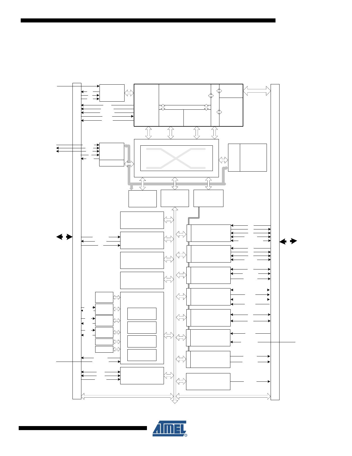
2. Overview
2.1
Blockdiagram
Figure 2-1.
Block diagram
TIMER/COUNTER
INTERRUPT
CONTROLLER
REAL TIME
COUNTER
PERIPHERAL
DMA
CONTROLLER
HSB-PB
BRIDGE B
HSB-PB
BRIDGE A
S
M
M
M
S
S
M
EXTERNAL
INTERRUPT
CONTROLLER
HIGH SPEED
BUS MATRIX
G
E
NE
R
A
L
P
URP
O
S
E
IOs
G
E
NE
R
A
L
P
URP
O
S
E
IO
s
PA
PB
A[2..0]
B[2..0]
CLK[2..0]
EXTINT[7..0]
KPS[7..0]
NMI
GCLK[3..0]
XIN32
XOUT32
XIN0
XOUT0
PA
PB
RESET_N
32 KHz
OSC
115 kHz
RCOSC
OSC0
PLL0
SERIAL
PERIPHERAL
INTERFACE
TWO-WIRE
INTERFACE
PD
C
PD
C
MISO, MOSI
NPCS[3..0]
SCL
SDA
USART1
PD
C
RXD
TXD
CLK
RTS, CTS
DSR, DTR, DCD, RI
USART0
USART2
PD
C
RXD
TXD
CLK
RTS, CTS
SYNCHRONOUS
SERIAL
CONTROLLER
PD
C
TX_CLOCK, TX_FRAME_SYNC
RX_DATA
TX_DATA
RX_CLOCK, RX_FRAME_SYNC
ANALOG TO
DIGITAL
CONVERTER
PD
C
AD[7..0]
ADVREF
WATCHDOG
TIMER
XIN1
XOUT1
OSC1
PLL1
SCK
JTAG
INTERFACE
MCKO
MDO[5..0]
MSEO[1..0]
EVTI_N
TCK
TDO
TDI
TMS
POWER
MANAGER
RESET
CONTROLLER
SLEEP
CONTROLLER
CLOCK
CONTROLLER
CLOCK
GENERATOR
CONFIGURATION REGISTERS BUS
PB
PB
HSB
HSB
S
F
L
ASH
CO
NTR
O
LL
ER
M
S
USB
INTERFACE
DMA
ID
VBOF
VBUS
D-
D+
EVTO_N
AVR32 UC
CPU
NEXUS
CLASS 2+
OCD
INSTR
INTERFACE
DATA
INTERFACE
M
E
M
O
RY
IN
TE
RFA
C
E
FAST GPIO
16/32/96 KB
SRAM
MEMORY PROTECTION UNIT
LOCAL BUS
INTERFACE
AUDIO
BITSTREAM
DAC
PD
C
DATA[1..0]
DATAN[1..0]
PULSE WIDTH
MODULATION
CONTROLLER
PWM[6..0]
64/128/
256/512 KB
FLASH
5
32059L–AVR32–01/2012
AT32UC3B
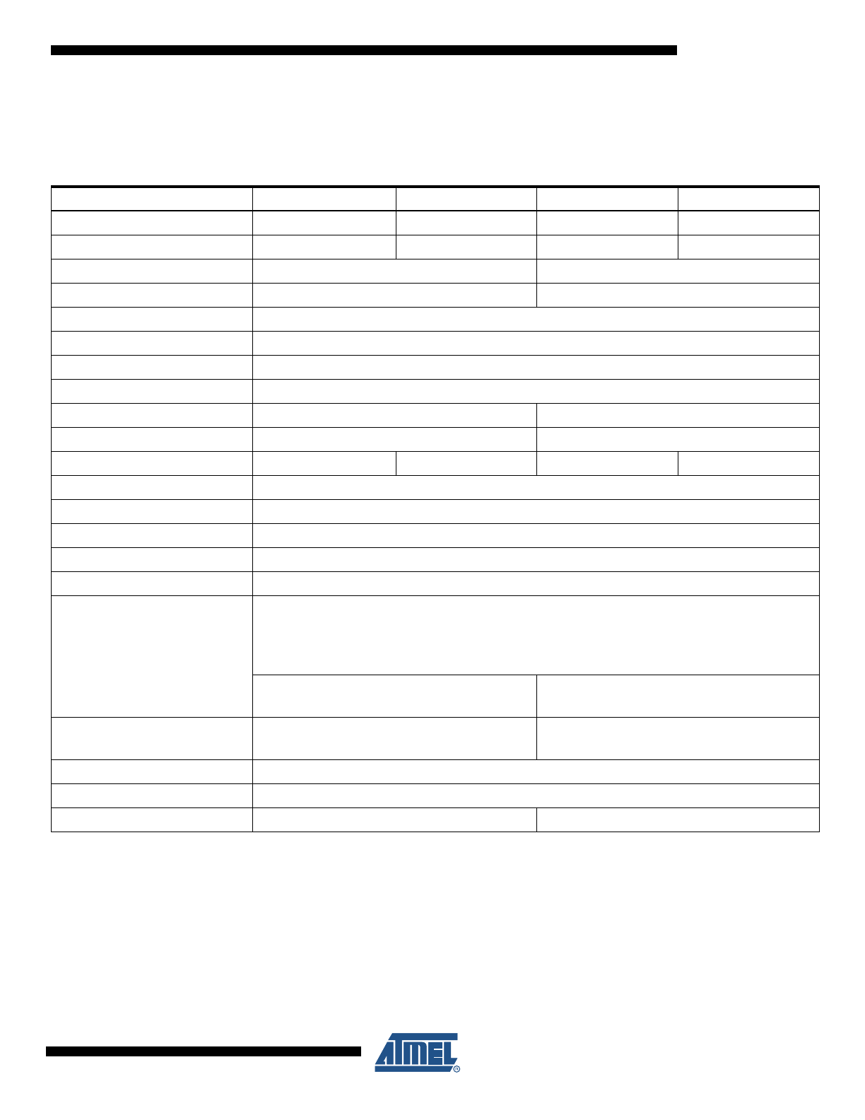
3. Configuration Summary
The table below lists all AT32UC3B memory and package configurations:
Table 3-1.
Configuration Summary
Feature
AT32UC3B0512
AT32UC3B0256/128/64
AT32UC3B1512
AT32UC3B1256/128/64
Flash
512 KB
256/128/64 KB
512 KB
256/128/64 KB
SRAM
96KB
32/32/16KB
96KB
32/16/16KB
GPIO
44
28
External Interrupts
8
6
TWI
1
USART
3
Peripheral DMA Channels
7
SPI
1
Full Speed USB
Mini-Host + Device
Device
SSC
1
0
Audio Bitstream DAC
1
0
1
0
Timer/Counter Channels
3
PWM Channels
7
Watchdog Timer
1
Real-Time Clock Timer
1
Power Manager
1
Oscillators
PLL 80-240 MHz (PLL0/PLL1)
Crystal Oscillators 0.4-20 MHz (OSC0)
Crystal Oscillator 32 KHz (OSC32K)
RC Oscillator 115 kHz (RCSYS)
Crystal Oscillators 0.4-20 MHz (OSC1)
10-bit ADC
number of channels
8
6
JTAG
1
Max Frequency
60 MHz
Package
TQFP64, QFN64
TQFP48, QFN48
6
32059L–AVR32–01/2012
AT32UC3B
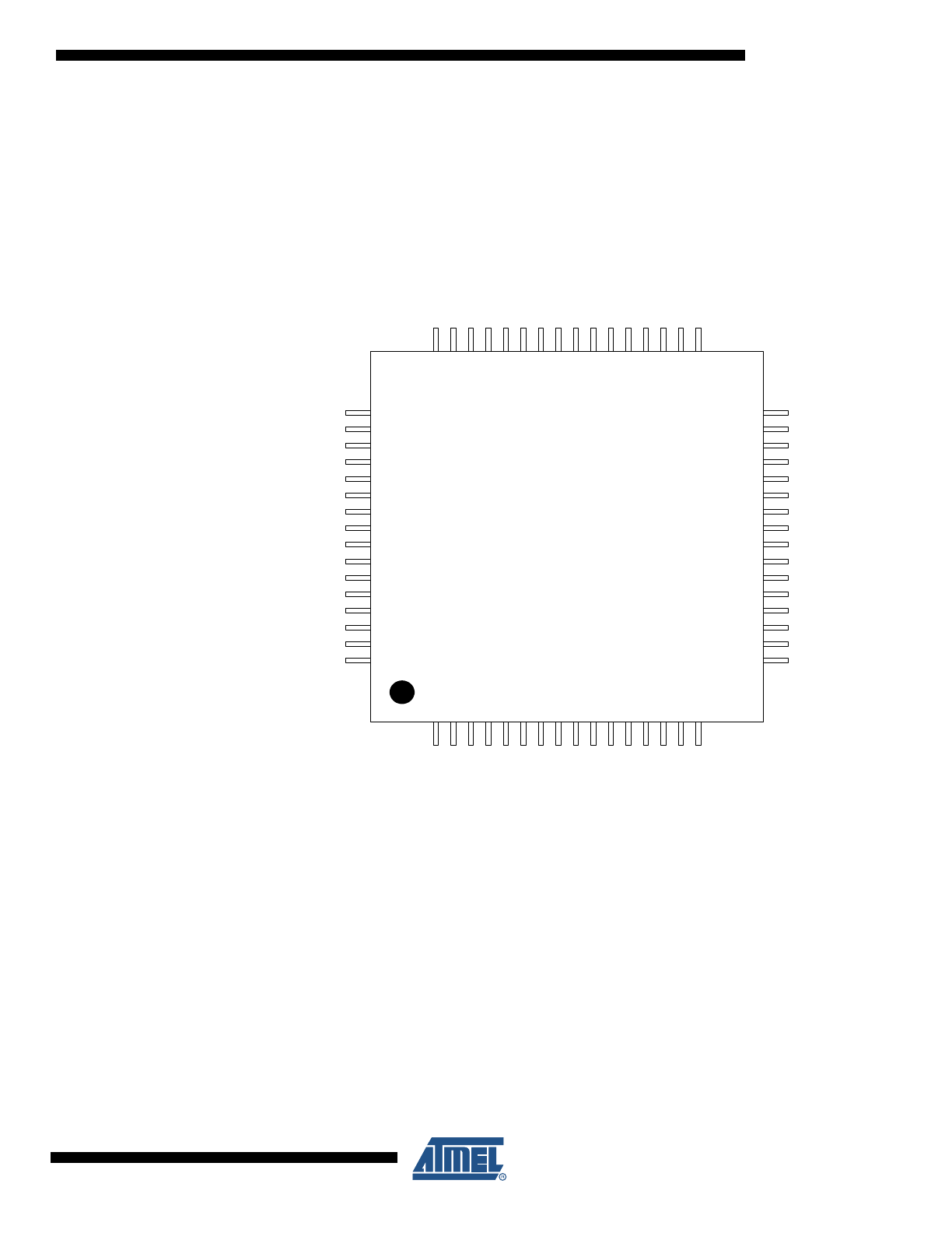
4. Package and Pinout
4.1
Package
The device pins are multiplexed with peripheral functions as described in the Peripheral Multi-
plexing on I/O Line section.
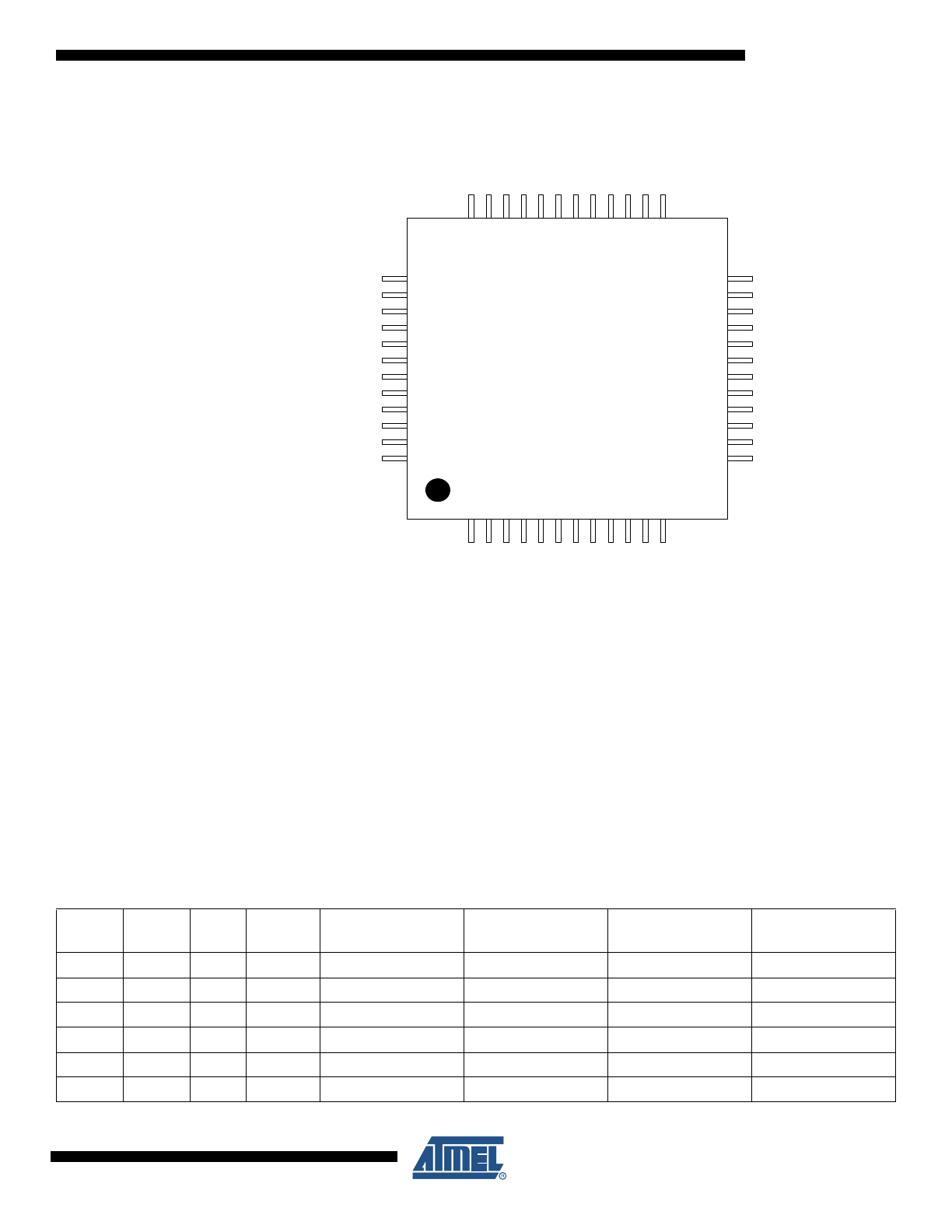
Figure 4-1.
TQFP64 / QFN64 Pinout
GND
1
TC
K
2
PA0
0
3
PA0
1
4
PA0
2
5
PB0
0
6
PB0
1
7
VDDCO
R
E
8
PA0
3
9
PA0
4
10
PA0
5
11
PA0
6
12
PA0
7
13
PA0
8
14
PA3
0
15
PA3
1
16
GNDANA
17
ADVREF
18
VDDANA
19
VDDOUT
20
VDDIN
21
VDDCORE
22
GND
23
PB02
24
PB03
25
PB04
26
PB05
27
PA09
28
PA10
29
PA11
30
PA12
31
VDDIO
32
VDDI
O
48
PA2
3
47
PA2
2
46
PA2
1
45
PA2
0
44
PB0
7
43
PA2
9
42
PA2
8
41
PA1
9
40
PA1
8
39
PB0
6
38
PA1
7
37
PA1
6
36
PA1
5
35
PA1
4
34
PA1
3
33
GND
49
DP
50
DM
51
VBUS
52
VDDPLL
53
PB08
54
PB09
55
VDDCORE
56
PB10
57
PB11
58
PA24
59
PA25
60
PA26
61
PA27
62
RESET_N
63
VDDIO
64
7
32059L–AVR32–01/2012
AT32UC3B
Figure 4-2.
TQFP48 / QFN48 Pinout
Note:
The exposed pad is not connected to anything internally, but should be soldered to ground to
increase board level reliability.
4.2
Peripheral Multiplexing on I/O lines
4.2.1
Multiplexed signals
Each GPIO line can be assigned to one of 4 peripheral functions; A, B, C or D (D is only avail-
able for UC3Bx512 parts). The following table define how the I/O lines on the peripherals A, B,C
or D are multiplexed by the GPIO.
GN
D
1
TC
K
2
PA
00
3
PA
01
4
PA
02
5
VD
DC
OR
E
6
PA
03
7
PA04
8
PA
05
9
PA
06
10
PA
07
11
PA
08
12
GNDANA
13
ADVREF
14
VDDANA
15
VDDOUT
16
VDDIN
17
VDDCORE
18
GND
19
PA09
20
PA10
21
PA11
22
PA12
23
VDDIO
24
VDD
IO
36
PA23
35
PA22
34
PA21
33
PA20
32
PA19
31
PA18
30
PA17
29
PA16
28
PA15
27
PA14
26
PA13
25
GND
37
DP
38
DM
39
VBUS
40
VDDPLL
41
VDDCORE
42
PA24
43
PA25
44
PA26
45
PA27
46
RESET_N
47
VDDIO
48
Table 4-1.
GPIO Controller Function Multiplexing
48-pin
64-pin
PIN
GPIO Pin
Function A
Function B
Function C
Function D
(only for UC3Bx512)
3
3
PA00
GPIO 0
4
4
PA01
GPIO 1
5
5
PA02
GPIO 2
7
9
PA03
GPIO 3
ADC - AD[0]
PM - GCLK[0]
USBB - USB_ID
ABDAC - DATA[0]
8
10
PA04
GPIO 4
ADC - AD[1]
PM - GCLK[1]
USBB - USB_VBOF
ABDAC - DATAN[0]
9
11
PA05
GPIO 5
EIC - EXTINT[0]
ADC - AD[2]
USART1 - DCD
ABDAC - DATA[1]

8
32059L–AVR32–01/2012
AT32UC3B
10
12
PA06
GPIO 6
EIC - EXTINT[1]
ADC - AD[3]
USART1 - DSR
ABDAC - DATAN[1]
11
13
PA07
GPIO 7
PWM - PWM[0]
ADC - AD[4]
USART1 - DTR
SSC -
RX_FRAME_SYNC
12
14
PA08
GPIO 8
PWM - PWM[1]
ADC - AD[5]
USART1 - RI
SSC - RX_CLOCK
20
28
PA09
GPIO 9
TWI - SCL
SPI0 - NPCS[2]
USART1 - CTS
21
29
PA10
GPIO 10
TWI - SDA
SPI0 - NPCS[3]
USART1 - RTS
22
30
PA11
GPIO 11
USART0 - RTS
TC - A2
PWM - PWM[0]
SSC - RX_DATA
23
31
PA12
GPIO 12
USART0 - CTS
TC - B2
PWM - PWM[1]
USART1 - TXD
25
33
PA13
GPIO 13
EIC - NMI
PWM - PWM[2]
USART0 - CLK
SSC - RX_CLOCK
26
34
PA14
GPIO 14
SPI0 - MOSI
PWM - PWM[3]
EIC - EXTINT[2]
PM - GCLK[2]
27
35
PA15
GPIO 15
SPI0 - SCK
PWM - PWM[4]
USART2 - CLK
28
36
PA16
GPIO 16
SPI0 - NPCS[0]
TC - CLK1
PWM - PWM[4]
29
37
PA17
GPIO 17
SPI0 - NPCS[1]
TC - CLK2
SPI0 - SCK
USART1 - RXD
30
39
PA18
GPIO 18
USART0 - RXD
PWM - PWM[5]
SPI0 - MISO
SSC -
RX_FRAME_SYNC
31
40
PA19
GPIO 19
USART0 - TXD
PWM - PWM[6]
SPI0 - MOSI
SSC - TX_CLOCK
32
44
PA20
GPIO 20
USART1 - CLK
TC - CLK0
USART2 - RXD
SSC - TX_DATA
33
45
PA21
GPIO 21
PWM - PWM[2]
TC - A1
USART2 - TXD
SSC -
TX_FRAME_SYNC
34
46
PA22
GPIO 22
PWM - PWM[6]
TC - B1
ADC - TRIGGER
ABDAC - DATA[0]
35
47
PA23
GPIO 23
USART1 - TXD
SPI0 - NPCS[1]
EIC - EXTINT[3]
PWM - PWM[0]
43
59
PA24
GPIO 24
USART1 - RXD
SPI0 - NPCS[0]
EIC - EXTINT[4]
PWM - PWM[1]
44
60
PA25
GPIO 25
SPI0 - MISO
PWM - PWM[3]
EIC - EXTINT[5]
45
61
PA26
GPIO 26
USBB - USB_ID
USART2 - TXD
TC - A0
ABDAC - DATA[1]
46
62
PA27
GPIO 27
USBB - USB_VBOF
USART2 - RXD
TC - B0
ABDAC - DATAN[1]
41
PA28
GPIO 28
USART0 - CLK
PWM - PWM[4]
SPI0 - MISO
ABDAC - DATAN[0]
42
PA29
GPIO 29
TC - CLK0
TC - CLK1
SPI0 - MOSI
15
PA30
GPIO 30
ADC - AD[6]
EIC - SCAN[0]
PM - GCLK[2]
16
PA31
GPIO 31
ADC - AD[7]
EIC - SCAN[1]
PWM - PWM[6]
6
PB00
GPIO 32
TC - A0
EIC - SCAN[2]
USART2 - CTS
7
PB01
GPIO 33
TC - B0
EIC - SCAN[3]
USART2 - RTS
24
PB02
GPIO 34
EIC - EXTINT[6]
TC - A1
USART1 - TXD
25
PB03
GPIO 35
EIC - EXTINT[7]
TC - B1
USART1 - RXD
26
PB04
GPIO 36
USART1 - CTS
SPI0 - NPCS[3]
TC - CLK2
27
PB05
GPIO 37
USART1 - RTS
SPI0 - NPCS[2]
PWM - PWM[5]
38
PB06
GPIO 38
SSC - RX_CLOCK
USART1 - DCD
EIC - SCAN[4]
ABDAC - DATA[0]
43
PB07
GPIO 39
SSC - RX_DATA
USART1 - DSR
EIC - SCAN[5]
ABDAC - DATAN[0]
54
PB08
GPIO 40
SSC -
RX_FRAME_SYNC
USART1 - DTR
EIC - SCAN[6]
ABDAC - DATA[1]
Table 4-1.
GPIO Controller Function Multiplexing
9
32059L–AVR32–01/2012
AT32UC3B
4.2.2
JTAG Port Connections
If the JTAG is enabled, the JTAG will take control over a number of pins, irrespective of the I/O
Controller configuration.
4.2.3
Nexus OCD AUX port connections
If the OCD trace system is enabled, the trace system will take control over a number of pins, irre-
spectively of the PIO configuration. Two different OCD trace pin mappings are possible,
depending on the configuration of the OCD AXS register. For details, see the AVR32 UC Tech-
nical Reference Manual.
4.2.4
Oscillator Pinout
The oscillators are not mapped to the normal A, B or C functions and their muxings are con-
trolled by registers in the Power Manager (PM). Please refer to the power manager chapter for
more information about this.
55
PB09
GPIO 41
SSC - TX_CLOCK
USART1 - RI
EIC - SCAN[7]
ABDAC - DATAN[1]
57
PB10
GPIO 42
SSC - TX_DATA
TC - A2
USART0 - RXD
58
PB11
GPIO 43
SSC -
TX_FRAME_SYNC
TC - B2
USART0 - TXD
Table 4-1.
GPIO Controller Function Multiplexing
Table 4-2.
JTAG Pinout
64QFP/QFN
48QFP/QFN
Pin name
JTAG pin
2
2
TCK
TCK
3
3
PA00
TDI
4
4
PA01
TDO
5
5
PA02
TMS
Table 4-3.
Nexus OCD AUX port connections
Pin
AXS=0
AXS=1
EVTI_N
PB05
PA14
MDO[5]
PB04
PA08
MDO[4]
PB03
PA07
MDO[3]
PB02
PA06
MDO[2]
PB01
PA05
MDO[1]
PB00
PA04
MDO[0]
PA31
PA03
EVTO_N
PA15
PA15
MCKO
PA30
PA13
MSEO[1]
PB06
PA09
MSEO[0]
PB07
PA10
10
32059L–AVR32–01/2012
AT32UC3B
4.3
High Drive Current GPIO
Ones of GPIOs can be used to drive twice current than other GPIO capability (see Electrical
Characteristics section).
5. Signals Description
The following table gives details on the signal name classified by peripheral.
Table 4-4.
Oscillator pinout
QFP48 pin
QFP64 pin
Pad
Oscillator pin
30
39
PA18
XIN0
41
PA28
XIN1
22
30
PA11
XIN32
31
40
PA19
XOUT0
42
PA29
XOUT1
23
31
PA12
XOUT32
Table 4-5.
High Drive Current GPIO
GPIO Name
PA20
PA21
PA22
PA23
Table 5-1.
Signal Description List
Signal Name
Function
Type
Active
Level
Comments
Power
VDDPLL
PLL Power Supply
Power
Input
1.65V to 1.95 V
VDDCORE
Core Power Supply
Power
Input
1.65V to 1.95 V
VDDIO
I/O Power Supply
Power
Input
3.0V to 3.6V
VDDANA
Analog Power Supply
Power
Input
3.0V to 3.6V
VDDIN
Voltage Regulator Input Supply
Power
Input
3.0V to 3.6V