
Features
•
High Performance, Low Power 32-Bit Atmel
®
AVR
®
Microcontroller
– Compact Single-cycle RISC Instruction Set Including DSP Instruction Set
– Read-Modify-Write Instructions and Atomic Bit Manipulation
– Performing 1.49 DMIPS / MHz
Up to 91 DMIPS Running at 66 MHz from Flash (1 Wait-State)
Up to 49 DMIPS Running at 33MHz from Flash (0 Wait-State)
– Memory Protection Unit
•
Multi-hierarchy Bus System
– High-Performance Data Transfers on Separate Buses for Increased Performance
– 15 Peripheral DMA Channels Improves Speed for Peripheral Communication
•
Internal High-Speed Flash
– 512K Bytes, 256K Bytes, 128K Bytes Versions
– Single Cycle Access up to 33 MHz
– Prefetch Buffer Optimizing Instruction Execution at Maximum Speed
– 4ms Page Programming Time and 8ms Full-Chip Erase Time
– 100,000 Write Cycles, 15-year Data Retention Capability
– Flash Security Locks and User Defined Configuration Area
•
Internal High-Speed SRAM, Single-Cycle Access at Full Speed
– 64K Bytes (512KB and 256KB Flash), 32K Bytes (128KB Flash)
•
External Memory Interface on AT32UC3A0 Derivatives
– SDRAM / SRAM Compatible Memory Bus (16-bit Data and 24-bit Address Buses)
•
Interrupt Controller
– Autovectored Low Latency Interrupt Service with Programmable Priority
•
System Functions
– Power and Clock Manager Including Internal RC Clock and One 32KHz Oscillator
– Two Multipurpose Oscillators and Two Phase-Lock-Loop (PLL) allowing
Independant CPU Frequency from USB Frequency
– Watchdog Timer, Real-Time Clock Timer
•
Universal Serial Bus (USB)
– Device 2.0 Full Speed and On-The-Go (OTG) Low Speed and Full Speed
– Flexible End-Point Configuration and Management with Dedicated DMA Channels
– On-chip Transceivers Including Pull-Ups
•
Ethernet MAC 10/100 Mbps interface
– 802.3 Ethernet Media Access Controller
– Supports Media Independent Interface (MII) and Reduced MII (RMII)
•
One Three-Channel 16-bit Timer/Counter (TC)
– Three External Clock Inputs, PWM, Capture and Various Counting Capabilities
•
One 7-Channel 16-bit Pulse Width Modulation Controller (PWM)
•
Four Universal Synchronous/Asynchronous Receiver/Transmitters (USART)
– Independant Baudrate Generator, Support for SPI, IrDA and ISO7816 interfaces
– Support for Hardware Handshaking, RS485 Interfaces and Modem Line
•
Two Master/Slave Serial Peripheral Interfaces (SPI) with Chip Select Signals
•
One Synchronous Serial Protocol Controller
– Supports I2S and Generic Frame-Based Protocols
•
One Master/Slave Two-Wire Interface (TWI), 400kbit/s I2C-compatible
•
One 8-channel 10-bit Analog-To-Digital Converter
•
16-bit Stereo Audio Bitstream
– Sample Rate Up to 50 KHz
32-Bit Atmel AVR
Microcontroller
AT32UC3A0512
AT32UC3A0256
AT32UC3A0128
AT32UC3A1512
AT32UC3A1256
AT32UC3A1128
Summary
32058KS–AVR32–01/12

2
AT32UC3A
•
On-Chip Debug System (JTAG interface)
– Nexus Class 2+, Runtime Control, Non-Intrusive Data and Program Trace
•
100-pin TQFP (69 GPIO pins), 144-pin LQFP (109 GPIO pins) , 144 BGA (109 GPIO pins)
•
5V Input Tolerant I/Os
•
Single 3.3V Power Supply or Dual 1.8V-3.3V Power Supply
32058KS–AVR32–01/12

3
AT32UC3A
1.
Description
The AT32UC3A is a complete System-On-Chip microcontroller based on the AVR32 UC RISC
processor running at frequencies up to 66 MHz. AVR32 UC is a high-performance 32-bit RISC
microprocessor core, designed for cost-sensitive embedded applications, with particular empha-
sis on low power consumption, high code density and high performance.
The processor implements a Memory Protection Unit (MPU) and a fast and flexible interrupt con-
troller for supporting modern operating systems and real-time operating systems. Higher
computation capabilities are achievable using a rich set of DSP instructions.
The AT32UC3A incorporates on-chip Flash and SRAM memories for secure and fast access.
For applications requiring additional memory, an external memory interface is provided on
AT32UC3A0 derivatives.
The Peripheral Direct Memory Access controller (PDCA) enables data transfers between periph-
erals and memories without processor involvement. PDCA drastically reduces processing
overhead when transferring continuous and large data streams between modules within the
MCU.
The PowerManager improves design flexibility and security: the on-chip Brown-Out Detector
monitors the power supply, the CPU runs from the on-chip RC oscillator or from one of external
oscillator sources, a Real-Time Clock and its associated timer keeps track of the time.
The Timer/Counter includes three identical 16-bit timer/counter channels. Each channel can be
independently programmed to perform frequency measurement, event counting, interval mea-
surement, pulse generation, delay timing and pulse width modulation.
The PWM modules provides seven independent channels with many configuration options
including polarity, edge alignment and waveform non overlap control. One PWM channel can
trigger ADC conversions for more accurate close loop control implementations.
The AT32UC3A also features many communication interfaces for communication intensive
applications. In addition to standard serial interfaces like UART, SPI or TWI, other interfaces like
flexible Synchronous Serial Controller, USB and Ethernet MAC are available.
The Synchronous Serial Controller provides easy access to serial communication protocols and
audio standards like I2S.
The Full-Speed USB 2.0 Device interface supports several USB Classes at the same time
thanks to the rich End-Point configuration. The On-The-GO (OTG) Host interface allows device
like a USB Flash disk or a USB printer to be directly connected to the processor.
The media-independent interface (MII) and reduced MII (RMII) 10/100 Ethernet MAC module
provides on-chip solutions for network-connected devices.
AT32UC3A integrates a class 2+ Nexus 2.0 On-Chip Debug (OCD) System, with non-intrusive
real-time trace, full-speed read/write memory access in addition to basic runtime control.
32058KS–AVR32–01/12
4
AT32UC3A
2.
Configuration Summary
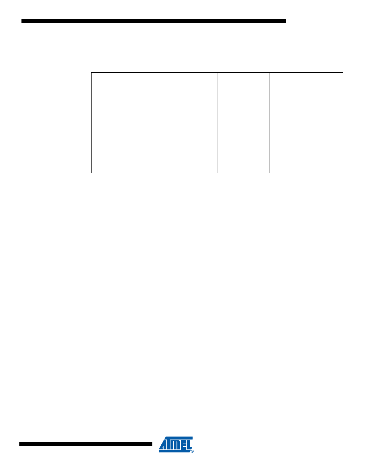
The table below lists all AT32UC3A memory and package configurations:
3.
Abbreviations
• GCLK: Power Manager Generic Clock
• GPIO: General Purpose Input/Output
• HSB: High Speed Bus
• MPU: Memory Protection Unit
• OCD: On Chip Debug
• PB: Peripheral Bus
• PDCA: Peripheral Direct Memory Access Controller (PDC) version A
• USBB: USB On-The-GO Controller version B
Device
Flash
SRAM
Ext. Bus Interface
Ethernet
MAC
Package
AT32UC3A0512
512 Kbytes
64 Kbytes
yes
yes
144 pin LQFP
144 pin BGA
AT32UC3A0256
256 Kbytes
64 Kbytes
yes
yes
144 pin LQFP
144 pin BGA
AT32UC3A0128
128 Kbytes
32 Kbytes
yes
yes
144 pin LQFP
144 pin BGA
AT32UC3A1512
512 Kbytes
64 Kbytes
no
yes
100 pin TQFP
AT32UC3A1256
256 Kbytes
64 Kbytes
no
yes
100 pin TQFP
AT32UC3A1128
128 Kbytes
32 Kbytes
no
yes
100 pin TQFP
32058KS–AVR32–01/12
5
AT32UC3A
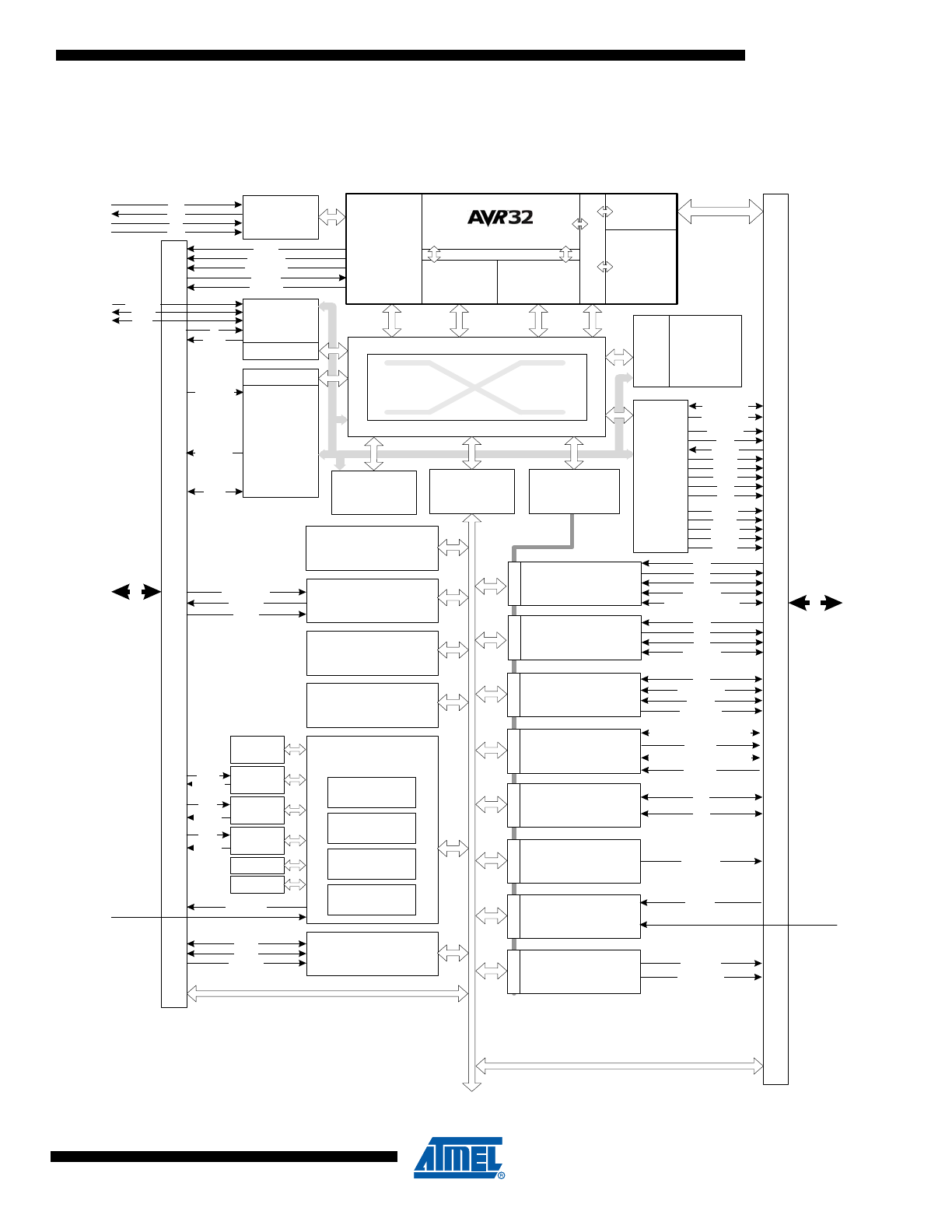
4.
Blockdiagram
Figure 4-1.
Blockdiagram
U C C P U
N E X U S
C LA S S 2+
O C D
IN S TR
IN TE R FAC E
D A TA
IN TE R FAC E
TIM E R /C O U N TE R
IN TE R R U PT
C O N TR O LLE R
R E AL TIM E
C O U N TE R
P ER IP H E R A L
D M A
C O NTR O LLER
512 K B
FLA SH
H S B-PB
B R ID G E B
H S B -P B
B R ID G E A
ME
MOR
Y
INT
E
RF
AC
E
S
M
M
M
M
M
S
S
S
S
S
M
E XTE R NA L
IN TER R U P T
C O N TR O LLE R
H IG H S PE E D
B U S M A TR IX
F A S T G P IO
G
EN
E
RA
L PUR
P
OSE IOs
64 KB
S R A M
GE
N
E
R
A
L P
U
RPOSE IO
s
P A
P B
P C
P X
A [2..0]
B[2..0]
CLK[2..0]
E X TIN T[7..0]
K P S[7..0]
N M I_N
G CLK [3..0]
X IN 32
XO UT32
X IN0
X O U T0
P A
P B
P C
P X
R E S E T_N
EXTERNAL
BUS INTE
R
F
AC
E
(SDRAM
& STATIC
MEM
O
RY
CO
N
T
RO
L
L
E
R
)
CAS
RAS
S D A 10
SD CK
SDC K E
S D C S 0
S D W E
NC S [3..0]
N RD
NW AIT
N W E 0
D A TA [15..0]
U S B
IN TER FA C E
D M A
ID
V B O F
V B U S
D -
D+
E TH E R N E T
M AC
D M A
32 K H z
O S C
115 kH z
R C O S C
O S C 0
P LL0
P U LS E W ID TH
M O D U LATIO N
C O N TR O LLE R
S ER IAL
PE R IP H ER A L
IN TE R FA C E 0/1
TW O -W IR E
IN TE R FAC E
PD
C
PD
C
PD
C
M IS O , M O S I
NP C S [3..1]
P W M [6..0]
S C L
S D A
U S AR T 1
PDC
R X D
TX D
CLK
R TS , C TS
D S R, DTR, D CD , RI
U S AR T 0
U S AR T 2
U S AR T 3
PD
C
R X D
TX D
CLK
R TS , C TS
S Y N C H R O N O U S
S ER IAL
C O N TR O LLE R
PD
C
TX _C LO C K , T X _F RA M E _S Y N C
R X _D A TA
T X_D A T A
RX _C LO C K , R X _F RA M E _S Y N C
A N ALO G TO
D IG ITA L
C O N V E R TE R
PD
C
A D[7..0]
A D V R E F
W A TC H D O G
TIM E R
X IN1
X O U T1
O S C 1
P LL1
S C K
JTA G
IN TER FA C E
M C K O
M D O [5..0]
M S E O [1..0]
E V TI_N
E V TO _N
TC K
TDO
TD I
TM S
P O W E R
M AN A G E R
R E S ET
C O N TR O LLE R
A DD R[23..0]
S LE E P
C O N TR O LLE R
C LO C K
C O N TR O LLE R
C LO C K
G E N E R ATO R
CO L,
CR S,
R X D[3..0],
R X_CLK ,
R X _DV ,
RX_E R
M DC ,
TX D [3..0],
TX _C LK,
TX _E N ,
TX _E R ,
S P E E D
M D IO
FL
ASH
C
O
NTROL
L
ER
C O N FIG U RA TIO N R E G IS TE R S B U S
M E M O R Y P R O TE C TIO N U NIT
P B
P B
H S B
H S
B
N W E 1
N W E 3
PB
A
PB
B
NPC S0
L O C A L B U S
INTE RFA CE
A U D IO
B ITSTR E AM
D A C
PD
C
DA TA [1..0]
D A TA N [1..0]
32058KS–AVR32–01/12

6
AT32UC3A
4.1
Processor and architecture
4.1.1
AVR32 UC CPU
•
32-bit load/store AVR32A RISC architecture.
– 15 general-purpose 32-bit registers.
– 32-bit Stack Pointer, Program Counter and Link Register reside in register file.
– Fully orthogonal instruction set.
– Privileged and unprivileged modes enabling efficient and secure Operating Systems.
– Innovative instruction set together with variable instruction length ensuring industry leading
code density.
– DSP extention with saturating arithmetic, and a wide variety of multiply instructions.
•
3 stage pipeline allows one instruction per clock cycle for most instructions.
– Byte, half-word, word and double word memory access.
– Multiple interrupt priority levels.
•
MPU allows for operating systems with memory protection.
4.1.2
Debug and Test system
•
IEEE1149.1 compliant JTAG and boundary scan
•
Direct memory access and programming capabilities through JTAG interface
•
Extensive On-Chip Debug features in compliance with IEEE-ISTO 5001-2003 (Nexus 2.0) Class 2+
– Low-cost NanoTrace supported.
•
Auxiliary port for high-speed trace information
•
Hardware support for 6 Program and 2 data breakpoints
•
Unlimited number of software breakpoints supported
•
Advanced Program, Data, Ownership, and Watchpoint trace supported
4.1.3
Peripheral DMA Controller
•
Transfers from/to peripheral to/from any memory space without intervention of the processor.
•
Next Pointer Support, forbids strong real-time constraints on buffer management.
•
Fifteen channels
– Two for each USART
– Two for each Serial Synchronous Controller
– Two for each Serial Peripheral Interface
– One for each ADC
– Two for each TWI Interface
4.1.4
Bus system
•
High Speed Bus (HSB) matrix with 6 Masters and 6 Slaves handled
– Handles Requests from the CPU Data Fetch, CPU Instruction Fetch, PDCA, USBB, Ethernet
Controller, CPU SAB, and to internal Flash, internal SRAM, Peripheral Bus A, Peripheral Bus
B, EBI.
– Round-Robin Arbitration (three modes supported: no default master, last
accessed default
master, fixed default master)
– Burst Breaking with Slot Cycle Limit
– One Address Decoder Provided per Master
32058KS–AVR32–01/12

7
AT32UC3A
•
Peripheral Bus A able to run on at divided bus speeds compared to the High Speed Bus
Figure 4-1
gives an overview of the bus system. All modules connected to the same bus use the
same clock, but the clock to each module can be individually shut off by the Power Manager.
The figure identifies the number of master and slave interfaces of each module connected to the
High Speed Bus, and which DMA controller is connected to which peripheral.
32058KS–AVR32–01/12
8
AT32UC3A
5.
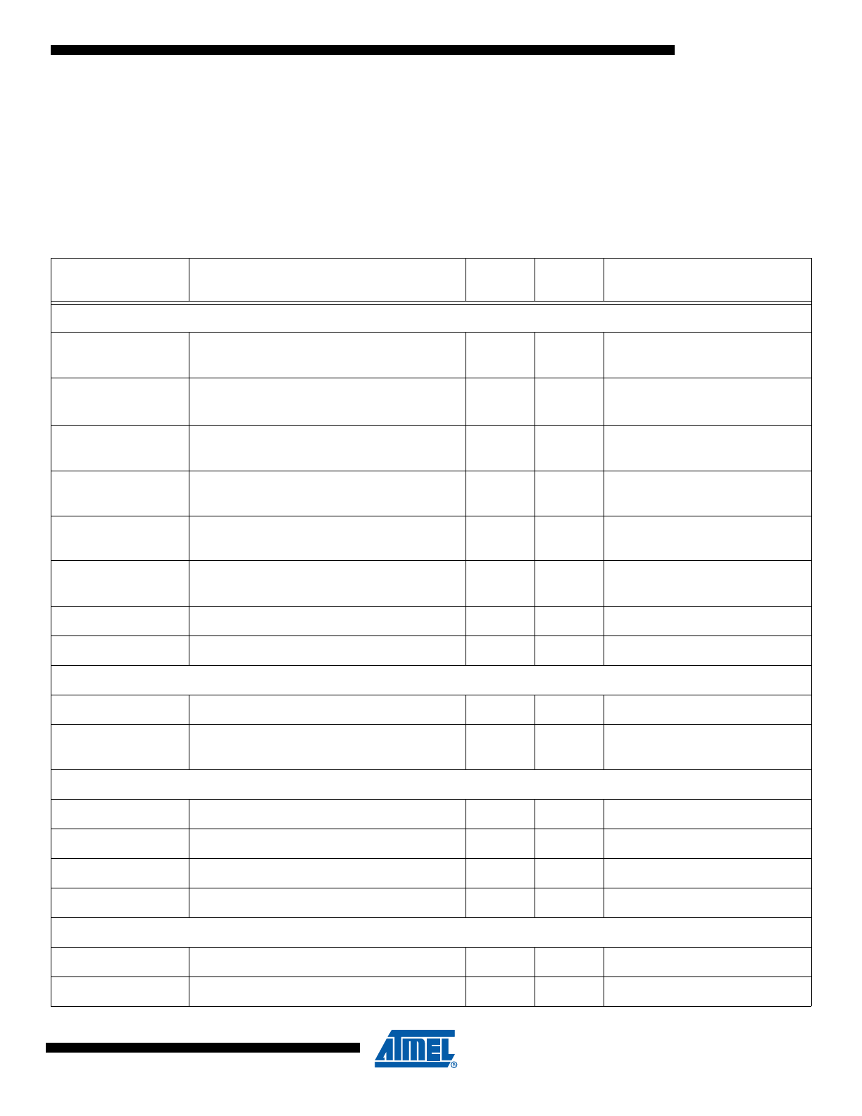
Signals Description
The following table gives details on the signal name classified by peripheral
The signals are multiplexed with GPIO pins as described in
”Peripheral Multiplexing on I/O lines”
on page 31
.
Table 5-1.
Signal Description List
Signal Name
Function
Type
Active
Level
Comments
Power
VDDPLL
Power supply for PLL
Power
Input
1.65V to 1.95 V
VDDCORE
Core Power Supply
Power
Input
1.65V to 1.95 V
VDDIO
I/O Power Supply
Power
Input
3.0V to 3.6V
VDDANA
Analog Power Supply
Power
Input
3.0V to 3.6V
VDDIN
Voltage Regulator Input Supply
Power
Input
3.0V to 3.6V
VDDOUT
Voltage Regulator Output
Power
Output
1.65V to 1.95 V
GNDANA
Analog Ground
Ground
GND
Ground
Ground
Clocks, Oscillators, and PLL’s
XIN0, XIN1, XIN32
Crystal 0, 1, 32 Input
Analog
XOUT0, XOUT1,
XOUT32
Crystal 0, 1, 32 Output
Analog
JTAG
TCK
Test Clock
Input
TDI
Test Data In
Input
TDO
Test Data Out
Output
TMS
Test Mode Select
Input
Auxiliary Port - AUX
MCKO
Trace Data Output Clock
Output
MDO0 - MDO5
Trace Data Output
Output
32058KS–AVR32–01/12
9
AT32UC3A
MSEO0 - MSEO1
Trace Frame Control
Output
EVTI_N
Event In
Output
Low
EVTO_N
Event Out
Output
Low
Power Manager - PM
GCLK0 - GCLK3
Generic Clock Pins
Output
RESET_N
Reset Pin
Input
Low
Real Time Counter - RTC
RTC_CLOCK
RTC clock
Output
Watchdog Timer - WDT
WDTEXT
External Watchdog Pin
Output
External Interrupt Controller - EIC
EXTINT0 - EXTINT7
External Interrupt Pins
Input
KPS0 - KPS7
Keypad Scan Pins
Output
NMI_N
Non-Maskable Interrupt Pin
Input
Low
Ethernet MAC - MACB
COL
Collision Detect
Input
CRS
Carrier Sense and Data Valid
Input
MDC
Management Data Clock
Output
MDIO
Management Data Input/Output
I/O
RXD0 - RXD3
Receive Data
Input
RX_CLK
Receive Clock
Input
RX_DV
Receive Data Valid
Input
RX_ER
Receive Coding Error
Input
SPEED
Speed
TXD0 - TXD3
Transmit Data
Output
TX_CLK
Transmit Clock or Reference Clock
Output
TX_EN
Transmit Enable
Output
TX_ER
Transmit Coding Error
Output
Table 5-1.
Signal Description List
Signal Name
Function
Type
Active
Level
Comments
32058KS–AVR32–01/12

10
AT32UC3A
External Bus Interface - HEBI
ADDR0 - ADDR23
Address Bus
Output
CAS
Column Signal
Output
Low
DATA0 - DATA15
Data Bus
I/O
NCS0 - NCS3
Chip Select
Output
Low
NRD
Read Signal
Output
Low
NWAIT
External Wait Signal
Input
Low
NWE0
Write Enable 0
Output
Low
NWE1
Write Enable 1
Output
Low
NWE3
Write Enable 3
Output
Low
RAS
Row Signal
Output
Low
SDA10
SDRAM Address 10 Line
Output
SDCK
SDRAM Clock
Output
SDCKE
SDRAM Clock Enable
Output
SDCS0
SDRAM Chip Select
Output
Low
SDWE
SDRAM Write Enable
Output
Low
General Purpose Input/Output 2 - GPIOA, GPIOB, GPIOC
P0 - P31
Parallel I/O Controller GPIOA
I/O
P0 - P31
Parallel I/O Controller GPIOB
I/O
P0 - P5
Parallel I/O Controller GPIOC
I/O
P0 - P31
Parallel I/O Controller GPIOX
I/O
Serial Peripheral Interface - SPI0, SPI1
MISO
Master In Slave Out
I/O
MOSI
Master Out Slave In
I/O
NPCS0 - NPCS3
SPI Peripheral Chip Select
I/O
Low
SCK
Clock
Output
Synchronous Serial Controller - SSC
RX_CLOCK
SSC Receive Clock
I/O
Table 5-1.
Signal Description List
Signal Name
Function
Type
Active
Level
Comments
32058KS–AVR32–01/12