

AT21CS01/AT21CS11
Single-Wire, I/O Powered 1-Kbit (128 x 8) Serial EEPROM
with a Unique, Factory-Programmed 64-Bit Serial Number
Features
•
Low
‑Voltage Operation:
–
AT21CS01 is self-powered via the 1.7V to 3.6V pull
‑up voltage on the SI/O line
–
AT21CS11 is self-powered via the 2.7V to 4.5V pull
‑up voltage on the SI/O line
•
Internally Organized as 128 Words of Eight Bits Each (1-Kbit)
•
Single-Wire Serial Interface with I
2
C Protocol Structure:
–
Device communication is achieved through a single I/O pin
•
Standard Speed and High-Speed Mode Options:
–
15.4 kbps maximum bit rate in Standard Speed mode (AT21CS01 only)
–
125 kbps maximum bit rate in High-Speed mode (AT21CS01 and AT21CS11)
•
8
‑Byte Page Write or Single Byte Writes Allowed
•
Discovery Response Feature for Quick Detection of Devices on the Bus
•
ROM Zone Support:
–
Device is segmented into four 256
‑bit zones, each of which can be permanently made
read
‑only (ROM)
•
256
‑bit Security Register:
–
Lower eight bytes contains a factory-programmed, read-only, 64
‑bit serial number that is
unique to all Microchip single
‑wire products
–
Next eight bytes are reserved for future use and will read FFh
–
Upper 16 bytes are user
‑programmable and permanently lockable
•
Self
‑Timed Write Cycle (5 ms maximum)
•
Manufacturer Identification Register:
–
Device responds with unique value for Microchip as well as density and revision information
•
High Reliability:
–
Endurance: 1,000,000 write cycles
–
Data retention: 100 years
–
IEC 61000-4-2 Level 4 ESD Compliant (±8 kV Contact, ±15 kV Air Discharge)
•
Green (Lead-free/Halide-free/RoHS Compliant) Package Options
•
Die Sale Options in Wafer Form and Tape and Reel
Packages
2-pad XSFN, 3-lead SOT23, 8-lead SOIC and 4-ball thin WLCSP.
©
2017 Microchip Technology Inc.
Datasheet
DS20005857A-page 1
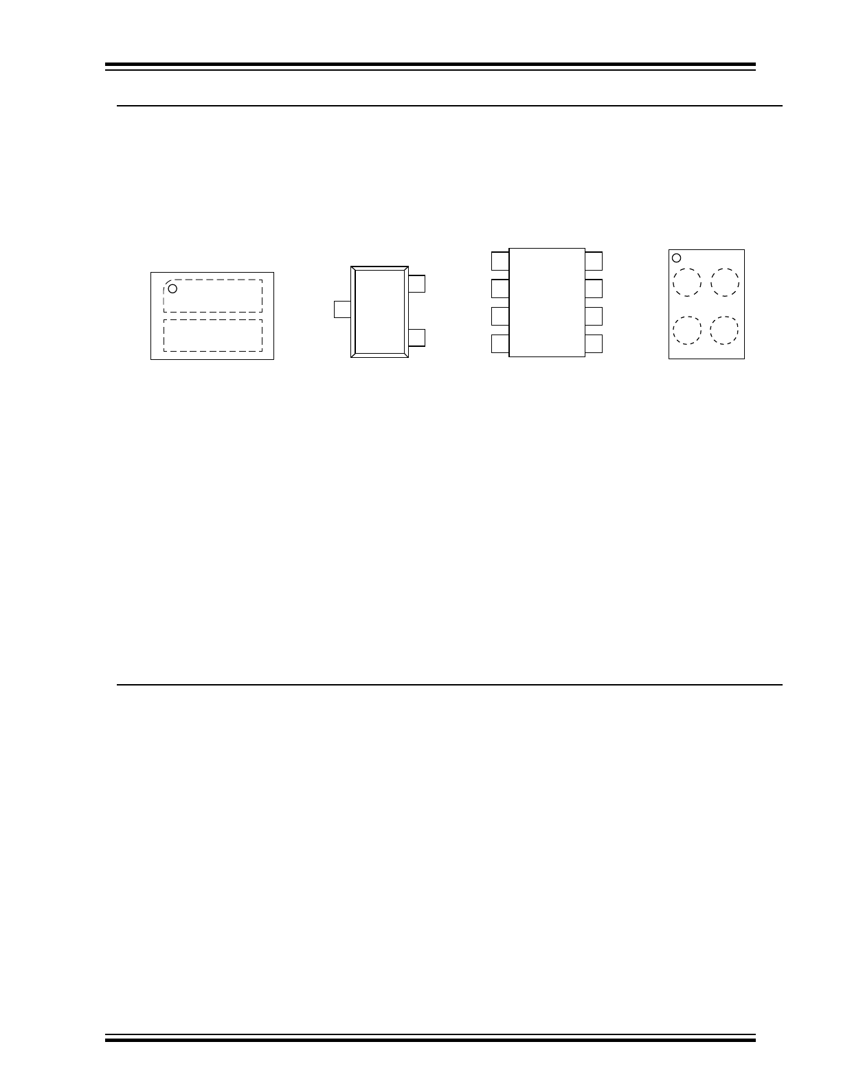
Package Types (not to scale)
8-lead SOIC
(Top View)
NC
1
2
3
4
8
7
6
5
NC
NC
GND
NC
NC
NC
SI/O
SI/O
GND
4-ball WLCSP
(Top View)
NC
NC
A1
A2
B1
B2
3
2
1
GND
SI/O
NC
3-lead SOT23
(Top View)
SI/O
GND
1
2
2-pad XSFN
(Top View)
Description
The AT21CS01/11 is a 2-pin memory (SI/O signal and Ground) that harvests energy from the signal pin to
power the integrated circuit. It provides 1,024 bits of Serial Electrically Erasable and Programmable Read-
Only Memory (SEEPROM) organized as 128 words of eight bits each.
The device is optimized to add configuration and use information in unpowered attachments using a two-point
mechanical connection that brings only one signal (SI/O) and GND to the unpowered attachment. Some
unpowered attachment application examples include analog sensor calibration data storage, ink and toner
printer cartridge identification, and management of after
‑market consumables. The device’s software
addressing scheme allows up to eight devices to share a common single
‑wire bus. The device is available in
space
‑saving package options and operates with an external pull‑up voltage from 1.7V to 3.6V on the SI/O
line (AT21CS01) or from 2.7V to 4.5V on the SI/O line (AT21CS11).
AT21CS01/AT21CS11
©
2017 Microchip Technology Inc.
Datasheet
DS20005857A-page 2
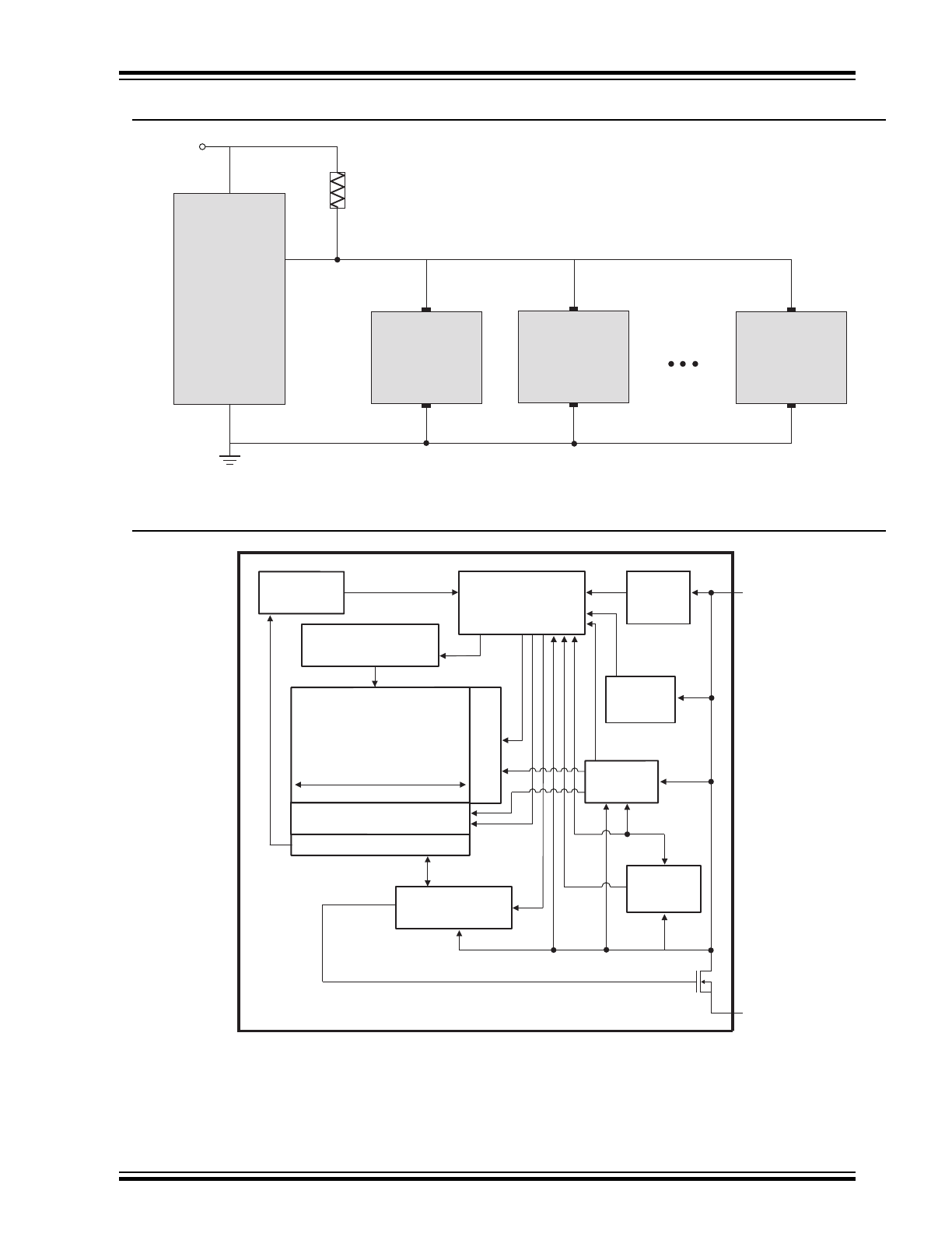
System Configuration Using Single-Wire Serial EEPROMs
Bus Master:
Microcontroller
Slave 0
AT21CSXX
GND
V
CC
GND
SI/O
R
PUP
(See Sections 1.3 and 1.4 for requirements.)
V
PUP
SI/O
Slave 1
AT21CSXX
GND
SI/O
Slave 7
AT21CSXX
GND
SI/O
Block Diagram
1 page
Internal
Timing
Generation
GND
Memory
System Control
Module
High Voltage
Generation Circuit
Data & ACK
Input/Output Control
Command
Control
Reset
Detection
D
OUT
D
IN
Device
Configuration
Latches
SI/O
Device
Power
Extraction
EEPROM Array
Column Decoder
Row Decoder
Data Register
AT21CS01/AT21CS11
©
2017 Microchip Technology Inc.
Datasheet
DS20005857A-page 3

Table of Contents
Features.......................................................................................................................... 1
Packages.........................................................................................................................1
Package Types (not to scale).......................................................................................... 2
Description.......................................................................................................................2
System Configuration Using Single-Wire Serial EEPROMs............................................3
Block Diagram................................................................................................................. 3
1. Electrical Characteristics........................................................................................... 6
1.1.
Absolute Maximum Ratings
(
1
)
...................................................................................................... 6
1.2.
AT21CS01/11 DC and AC Operating Range................................................................................6
1.3.
AT21CS01 DC Characteristics
(
1
)
..................................................................................................6
1.4.
AT21CS11 DC Characteristics
(
1
)
.................................................................................................. 7
1.5.
AT21CS01/11 AC Characteristics.................................................................................................8
2. Pin Descriptions.......................................................................................................11
2.1.
No Connect.................................................................................................................................11
2.2.
Serial Input and Output...............................................................................................................11
3. Device Operation and Communication....................................................................12
3.1.
Single-Wire Bus Transactions.................................................................................................... 12
4. Device Addressing and I
2
C Protocol Emulation...................................................... 18
4.1.
Memory Organization................................................................................................................. 18
5. Available Opcodes...................................................................................................20
5.1.
EEPROM Access (Opcode Ah)..................................................................................................20
5.2.
Security Register Access (Opcode Bh)...................................................................................... 20
5.3.
Lock Security Register (Opcode 2h).......................................................................................... 20
5.4.
ROM Zone Register Access (Opcode 7h)..................................................................................20
5.5.
Freeze ROM Zone State (Opcode 1h)....................................................................................... 21
5.6.
Manufacturer ID Read (Opcode Ch).......................................................................................... 21
5.7.
Standard Speed Mode (Opcode Dh)..........................................................................................21
5.8.
High-Speed Mode (Opcode Eh)................................................................................................. 21
6. Write Operations......................................................................................................22
6.1.
Device Behavior During Internal Write Cycle............................................................................. 22
6.2.
Byte Write...................................................................................................................................22
6.3.
Page Write..................................................................................................................................23
6.4.
Writing to the Security Register..................................................................................................23
6.5.
Locking the Security Register.....................................................................................................24
6.6.
Setting the Device Speed...........................................................................................................25
AT21CS01/AT21CS11
©
2017 Microchip Technology Inc.
Datasheet
DS20005857A-page 4

7. Read Operations..................................................................................................... 27
7.1.
Current Address Read within the EEPROM...............................................................................27
7.2.
Random Read within the EEPROM........................................................................................... 28
7.3.
Sequential Read within the EEPROM........................................................................................ 28
7.4.
Read Operations in the Security Register.................................................................................. 29
7.5.
Manufacturer ID Read................................................................................................................ 30
8. ROM Zones............................................................................................................. 32
8.1.
ROM Zone Size and ROM Zone Registers................................................................................ 32
8.2.
Programming and Reading the ROM Zone Registers................................................................32
8.3.
Device Response to a Write Command Within an Enabled ROM Zone.................................... 34
9. Device Default Condition from Microchip................................................................ 36
10. Packaging Information.............................................................................................37
10.1. Package Marking Information.....................................................................................................37
11. Revision History.......................................................................................................42
The Microchip Web Site................................................................................................ 43
Customer Change Notification Service..........................................................................43
Customer Support......................................................................................................... 43
Product Identification System........................................................................................44
Microchip Devices Code Protection Feature................................................................. 45
Legal Notice...................................................................................................................45
Trademarks................................................................................................................... 45
Quality Management System Certified by DNV.............................................................46
Worldwide Sales and Service........................................................................................47
AT21CS01/AT21CS11
©
2017 Microchip Technology Inc.
Datasheet
DS20005857A-page 5

1.
Electrical Characteristics
1.1
Absolute Maximum Ratings
(
1
)
Temperature under bias
-55°C to +125°C
Storage temperature
-65°C to +150°C
Voltage on any pin with respect to ground
-0.6V to V
PUP
+0.5V
DC output current
15.0 mA
Note:
1.
Stresses beyond those listed under “Absolute Maximum Ratings” may cause permanent damage to
the device. This is a stress rating only and functional operation of the device at these or any other
conditions beyond those indicated in the operational sections of this specification are not implied.
Exposure to absolute maximum rating conditions for extended periods may affect device reliability.
1.2
AT21CS01/11 DC and AC Operating Range
AT21CS01
AT21CS11
Operating Temperature (Case)
Industrial Temperature Range
-40°C to +85°C -40°C to +85°C
V
PUP
Voltage tied to SI/O
Voltage Range
1.7V to 3.6V
2.7V to 4.5V
1.3
AT21CS01 DC Characteristics
(
1
)
Parameter
Symbol
Minimum
Typical
(
2
)
Maximum
Units
Test Conditions
Pull-up Voltage
V
PUP
1.7
—
3.6
V
High-Speed
mode
2.7
—
3.6
V
Standard Speed
mode
Pull-up Resistance
R
PUP
130
—
200
Ω
V
PUP
= 1.7V
0.2
—
1.8
kΩ
V
PUP
= 2.7V
0.33
—
4
kΩ
V
PUP
= 3.6V
Active Current, Read
I
A1
—
0.08
0.3
mA
V
PUP
= 3.6V;
SI/O = V
PUP
Active Current, Write
I
A2
—
0.20
0.5
mA
V
PUP
= 3.6V
Standby Current
I
SB
—
0.6
1.5
µA
V
PUP
= 1.8V
(
3
)
;
SI/O = V
PUP
—
0.7
2.5
µA
V
PUP
= 3.6V
Input Low Level
(
3
)(
4
)
V
IL
–0.6
—
0.5
V
Input High Level
(
3
)(
4
)
V
IH
V
PUP
x 0.7
—
V
PUP
+ 0.5
V
AT21CS01/AT21CS11
©
2017 Microchip Technology Inc.
Datasheet
DS20005857A-page 6

Parameter
Symbol
Minimum
Typical
(
2
)
Maximum
Units
Test Conditions
SI/O Hysteresis
(
3
)(
4
)(
5
)
V
HYS
0.128
—
1.17
V
Output Low Level
V
OL
0
—
0.4
V
I
OL
= 4 mA
Bus Capacitance
C
BUS
—
—
1000
pF
Note:
1.
Parameters are applicable over the operating range in
AT21CS01/11 DC and AC Operating Range
,
unless otherwise noted.
2.
Typical values characterized at T
A
= +25°C unless otherwise noted.
3.
This parameter is characterized but is not 100% tested in production.
4.
V
IH
, V
IL
, and V
HYS
are a function of the internal supply voltage, which is a function of V
PUP
, R
PUP
,
C
BUS
, and timing used. Use of a lower V
PUP
, higher R
PUP
, higher C
BUS
, and shorter t
RCV
creates
lower V
IH
, V
IL
and V
HYS
values.
5.
Once V
IH
is crossed on a rising edge of SI/O, the voltage on SI/O must drop at least by V
HYS
to be
detected as a logic ‘0’.
1.4
AT21CS11 DC Characteristics
(
1
)
Parameter
Symbol
Minimum
Typical
(
2
)
Maximum
Units
Test Conditions
Pull-up Voltage
V
PUP
2.7
—
4.5
V
High-Speed
mode
Pull-up Resistance
R
PUP
0.2
—
1.8
kΩ
V
PUP
= 2.7V
0.4
—
5.4
kΩ
V
PUP
= 4.5V
Active Current, Read
I
A1
—
0.08
0.3
mA
V
PUP
= 4.5V;
SI/O = V
PUP
Active Current, Write
I
A2
—
0.20
0.5
mA
V
PUP
= 4.5V
Standby Current
I
SB
—
0.6
1.5
µA
V
PUP
= 2.7V
(
3
)
;
SI/O = V
PUP
—
0.7
3.0
µA
V
PUP
= 4.5V;
SI/O = V
PUP
Input Low Level
(
3
)(
4
)
V
IL
–0.6
—
0.5
V
Input High Level
(
3
)(
4
)
V
IH
V
PUP
x 0.7
—
V
PUP
+ 0.5
V
SI/O Hysteresis
(
3
)(
4
)(
5
)
V
HYS
0.128
—
1.4
V
Output Low Level
V
OL
0
—
0.4
V
I
OL
= 4 mA
Bus Capacitance
C
BUS
—
—
1000
pF
Note:
1.
Parameters are applicable over the operating range in
AT21CS01/11 DC and AC Operating Range
,
unless otherwise noted.
2.
Typical values characterized at T
A
= +25°C unless otherwise noted.
3.
This parameter is characterized but is not 100% tested in production.
AT21CS01/AT21CS11
©
2017 Microchip Technology Inc.
Datasheet
DS20005857A-page 7

4.
V
IH
, V
IL
, and V
HYS
are a function of the internal supply voltage, which is a function of V
PUP
, R
PUP
,
C
BUS
, and timing used. Use of a lower V
PUP
, higher R
PUP
, higher C
BUS
, and shorter t
RCV
creates
lower V
IH
, V
IL
and V
HYS
values.
5.
Once V
IH
is crossed on a rising edge of SI/O, the voltage on SI/O must drop at least by V
HYS
to be
detected as a logic ‘0’.
1.5
AT21CS01/11 AC Characteristics
1.5.1
Reset and Discovery Response Timing
Parameter and Condition
(
1
)(
2
)
Symbol
Standard
Speed
(
3
)(
4
)
High Speed
Units
Min.
Max.
Min.
Max.
Reset Low Time, Device in Inactive
State
t
RESET
480
—
48
—
µs
Discharge Low Time, Device in Active
Write Cycle (t
WR
)
t
DSCHG
150
—
150
—
µs
Reset Recovery Time
t
RRT
N/A
N/A
8
—
µs
Discovery Response Request
t
DRR
N/A
N/A
1
2 - t
PUP
(
5
)
µs
Discovery Response Acknowledge
Time
t
DACK
N/A
N/A
8
24
µs
Master Strobe Discovery Response
Time
t
MSDR
N/A
N/A
2
6
µs
SI/O High Time for Start/Stop
Condition
t
HTSS
N/A
N/A
150
—
µs
Note:
1.
Parameters applicable over operating range in
AT21CS01/11 DC and AC Operating Range
, unless
otherwise noted.
2.
AC measurement conditions for the table above:
–
Loading capacitance on SI/O: 100 pF
–
R
PUP
(bus line pull-up resistor to V
PUP
): 1 kΩ; V
PUP
: 2.7V
3.
Due to the fact that the device will default to High-Speed mode upon Reset, the Reset and
Discovery Response Timing after t
RESET
does not apply for Standard Speed mode. High-Speed
mode timing applies in all cases after t
RESET
.
4.
Standard Speed is not available on the AT21CS11.
5.
t
PUP
is the time required once the SI/O line is released to be pulled up from V
IL
to V
IH
. This value is
application specific and is a function of the loading capacitance on the SI/O line as well as the R
PUP
chosen. Limits for these values are provided in
AT21CS01 DC Characteristics(1)
and
AT21CS11
DC Characteristics(1)
.
AT21CS01/AT21CS11
©
2017 Microchip Technology Inc.
Datasheet
DS20005857A-page 8

1.5.2
Data Communication Timing
Parameter and Condition
(
1
)(
2
)
Symbol Frame Type
Standard
Speed
(
3
)
High Speed
Units
Min.
Max.
Min.
Max.
Bit Frame Duration
t
BIT
Input and
Output Bit
Frame
40
100
t
LOW0
+
t
PUP
(
4
)
+
t
RCV
25
µs
SI/O High Time for Start/Stop
Condition
t
HTSS
Input Bit
Frame
600
—
150
—
µs
SI/O Low Time, Logic ‘0’
Condition
t
LOW0
Input Bit
Frame
24
64
6
16
µs
SI/O Low Time, Logic ‘1’
Condition
t
LOW1
Input Bit
Frame
4
8
1
2
µs
Master SI/O Low Time During
Read
t
RD
Output Bit
Frame
4
8 -
t
PUP
(
4
)
1
2 -
t
PUP
(
4
)
µs
Master Read Strobe Time
t
MRS
Output Bit
Frame
t
RD
+
t
PUP
(
4
)
8
t
RD
+
t
PUP
(
4
)
2
µs
Data Output Hold Time (Logic
‘0’)
t
HLD0
Output Bit
Frame
8
24
2
6
µs
Slave Recovery Time
t
RCV
Input and
Output Bit
Frame
8
—
2
(
5
)
—
µs
Noise Filtering Capability on
SI/O
t
NOISE
Input Bit
Frame
0.5
—
—
—
µs
Note:
1.
Parameters applicable over operating range in
AT21CS01/11 DC and AC Operating Range
, unless
otherwise noted.
2.
AC measurement conditions for the table above:
–
Loading capacitance on SI/O: 100 pF
–
R
PUP
(bus line pull-up resistor to V
PUP
): 1 kΩ; V
PUP
: 2.7V
3.
Standard Speed is not available on the AT21CS11.
4.
t
PUP
is the time required once the SI/O line is released to be pulled up from V
IL
to V
IH
. This value is
application specific and is a function of the loading capacitance on the SI/O line as well as the R
PUP
chosen. Limits for these values are provided in
AT21CS01 DC Characteristics(1)
.
5.
The system designer must select an combination of R
PUP
, C
BUS
, and t
BIT
such that the minimum
t
RCV
is satisfied. The relationship of t
RCV
within the bit frame can be expressed by the following
formula: t
BIT
= t
LOW0
+ t
PUP
+ t
RCV
.
AT21CS01/AT21CS11
©
2017 Microchip Technology Inc.
Datasheet
DS20005857A-page 9

1.5.3
EEPROM Cell Performance Characteristics
Operation
Min.
Max.
Units
Test Condition
Write Cycle Time
(t
WR
)
—
5
ms
V
PUP
(min.) < V
PUP
< V
PUP
(max.),
T
A
= 25°C, Byte or Page Write mode
Write Endurance
(
1
)
1,000,000
—
Write Cycles
V
PUP
(min.) < V
PUP
< V
PUP
(max.),
T
A
= 25°C, Byte or Page Write mode
Data Retention
(
2
)
100
—
Years
V
PUP
(min.) < V
PUP
< V
PUP
(max.),
T
A
= 55°C
Note:
1.
Write endurance performance is determined through characterization and the qualification process.
2.
The data retention capability is determined through qualification and checked on each device in
production.
AT21CS01/AT21CS11
©
2017 Microchip Technology Inc.
Datasheet
DS20005857A-page 10