
2003-2012 Microchip Technology Inc.
DS21797L-page 1
93AA86A/B/C, 93LC86A/B/C,
93C86A/B/C
Device Selection Table
Features:
• Low-Power CMOS Technology
• ORG Pin to Select Word Size for ‘86C’ Version
• 2048 x 8-bit Organization ‘A’ Devices (no ORG)
• 1024 x 16-bit Organization ‘B’ Devices (no ORG)
• Program Enable Pin to Write-Protect the Entire
Array (‘86C’ version only)
• Self-tImed Erase/Write Cycles (including
Auto-Erase)
• Automatic Erase All (ERAL) before Write All
(WRAL)
• Power-On/Off Data Protection Circuitry
• Industry Standard 3-Wire Serial I/O
• Device Status Signal (Ready/
Busy
)
• Sequential Read Function
• 1,000,000 E/W Cycles
• Data Retention > 200 Years
• Pb-free and RoHS Compliant
• Temperature Ranges Supported:
Pin Function Table
Description:
The Microchip Technology Inc. 93XX86A/B/C devices
are 16K bit low-voltage serial Electrically Erasable
PROMs (EEPROM). Word-selectable devices such as
the 93XX86C are dependent upon external logic
levels driving the ORG pin to set word size. The
93XX86A devices provide dedicated 8-bit memory
organization, while the 93XX86B devices provide
dedicated 16-bit memory organization. A Program
Enable (PE) pin allows the user to write-protect the
entire memory array. Advanced CMOS technology
makes these devices ideal for low-power, nonvolatile
memory applications. The entire 93XX Series is
available in standard packages including 8-lead PDIP
and SOIC, and advanced packaging including 8-lead
MSOP, 6-lead SOT-23, 8-lead 2x3 DFN/TDFN and 8-
lead TSSOP. All packages are Pb-free (Matte Tin)
finish.
Part
Number
V
CC
Range
ORG Pin
PE Pin
Word Size
Temp Ranges
Packages
93AA86A
1.8-5.5
No
No
8-bit
I
P, SN, ST, MS, OT
93AA86B
1.8-5-5
No
No
16-bit
I
P, SN, ST, MS, OT
93LC86A
2.5-5.5
No
No
8-bit
I, E
P, SN, ST, MS, OT
93LC86B
2.5-5.5
No
No
16-bit
I, E
P, SN, ST, MS, OT
93C86A
4.5-5.5
No
No
8-bit
I, E
P, SN, ST, MS, OT
93C86B
4.5-5.5
No
No
16-bit
I, E
P, SN, ST, MS, OT
93AA86C
1.8-5.5
Yes
Yes
8- or 16-bit
I
P, SN, ST, MS, MC, MN
93LC86C
2.5-5.5
Yes
Yes
8- or 16-bit
I, E
P, SN, ST, MS, MC, MN
93C86C
4.5-5.5
Yes
Yes
8- or 16-bit
I, E
P, SN, ST, MS, MC, MN
- Industrial (I)
-40°C to +85°C
- Automotive (E)-40°C to +125°C
Name
Function
CS
Chip Select
CLK
Serial Data Clock
DI
Serial Data Input
DO
Serial Data Output
V
SS
Ground
PE
Program Enable – 93XX86C only
ORG
Memory Configuration – 93XX86C only
V
CC
Power Supply
16K Microwire Compatible Serial EEPROM
93AA86A/B/C, 93LC86A/B/C, 93C86A/B/C
DS21797L-page 2
2003-2012 Microchip Technology Inc.
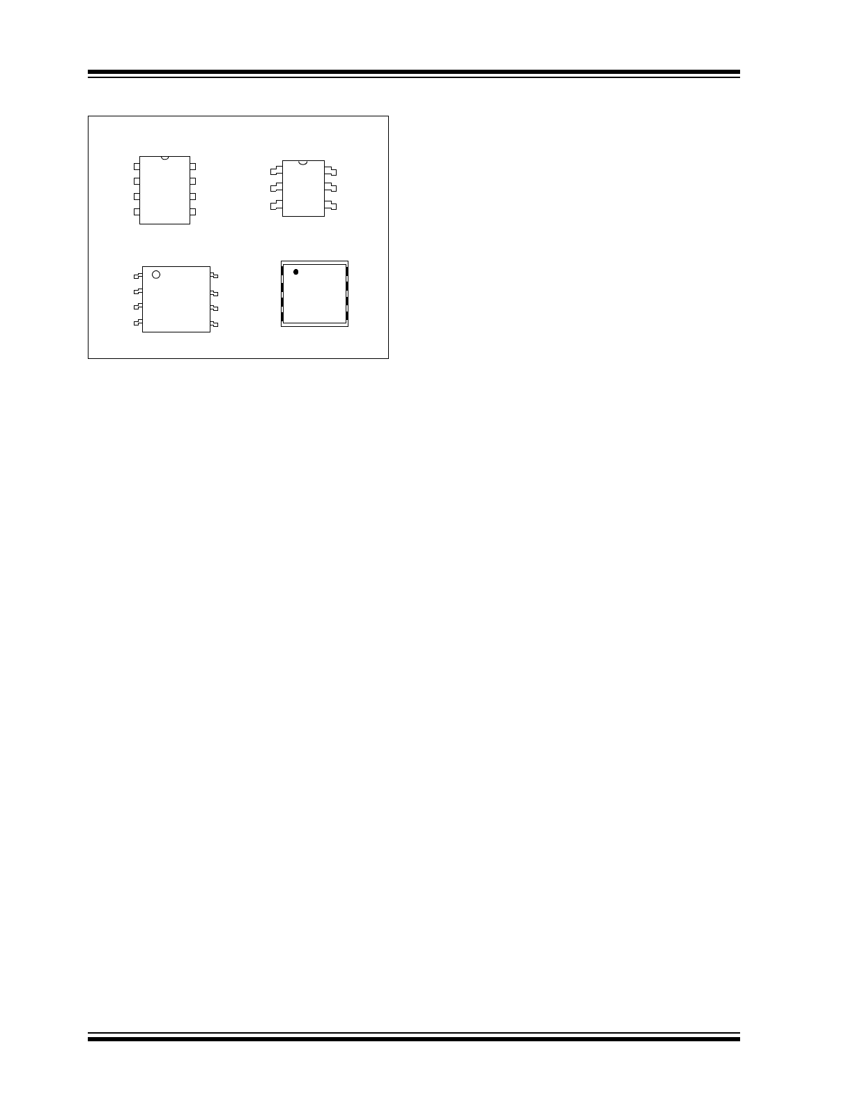
Package Types (not to scale)
CS
CLK
DI
DO
1
2
3
4
8
7
6
5
V
CC
PE
(1)
ORG
(1)
V
SS
PDIP/SOIC
(P, SN)
TSSOP/MSOP
CS
CLK
DI
DO
1
2
3
4
8
7
6
5
V
CC
PE
(1)
ORG
(1)
V
SS
(ST, MS)
SOT-23
DO
V
SS
DI
1
2
3
6
5
4
V
CC
CS
CLK
(OT)
DFN/TDFN
CS
CLK
DI
DO
PE
ORG
V
SS
V
CC
8
7
6
5
1
2
3
4
(MC, MN)
Note 1: 93XX86C only.
2003-2012 Microchip Technology Inc.
DS21797L-page 3
93AA86A/B/C, 93LC86A/B/C, 93C86A/B/C
1.0
ELECTRICAL CHARACTERISTICS
Absolute Maximum Ratings
(†)
V
CC
............................................................................................................................................................................. 7.0V
All inputs and outputs w.r.t. V
SS
..........................................................................................................-0.6V to V
CC
+1.0V
Storage temperature ............................................................................................................................... -65°C to +150°C
Ambient temperature with power applied................................................................................................-40°C to +125°C
ESD protection on all pins
4 kV
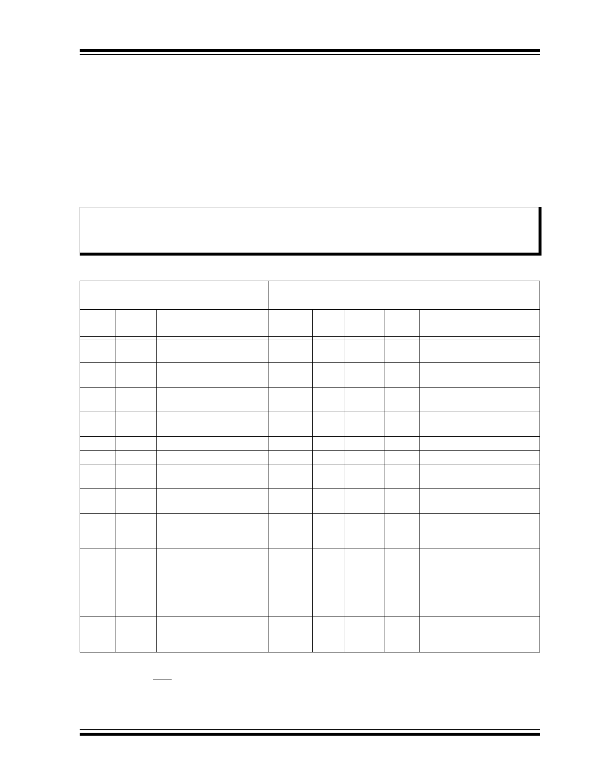
TABLE 1-1:
DC CHARACTERISTICS
Note:
†
NOTICE: Stresses above those listed under “Absolute Maximum Ratings” may cause permanent dam-
age to the device. This is a stress rating only and functional operation of the device at those or any other
conditions above those indicated in the operational listings of this specification is not implied. Exposure to
maximum rating conditions for extended periods may affect device reliability.
All parameters apply over the specified
ranges unless otherwise noted.
Industrial (I):
T
A
= -40°C to +85°C, V
CC
= +1.8V to 5.5V
Automotive (E): T
A
= -40°C to +125°C, V
CC
= +2.5V to 5.5V
Param.
No.
Symbol
Parameter
Min.
Typ.
Max.
Units
Conditions
D1
V
IH
1
V
IH
2
High-level input voltage
2.0
0.7 V
CC
—
—
V
CC
+1
V
CC
+1
V
V
V
CC
2.7V
V
CC
< 2.7V
D2
V
IL
1
V
IL
2
Low-level input voltage
-0.3
-0.3
—
—
0.8
0.2 V
CC
V
V
V
CC
2.7V
V
CC
< 2.7V
D3
V
OL
1
V
OL
2
Low-level output voltage
—
—
—
—
0.4
0.2
V
V
I
OL
= 2.1 mA, V
CC
= 4.5V
I
OL
= 100
A, V
CC
= 2.5V
D4
V
OH
1
V
OH
2
High-level output voltage
2.4
V
CC
- 0.2
—
—
—
—
V
V
I
OH
= -400
A, V
CC
= 4.5V
I
OH
= -100
A, V
CC
= 2.5V
D5
I
LI
Input leakage current
—
—
±1
A
V
IN
= V
SS
or V
CC
D6
I
LO
Output leakage current
—
—
±1
A
V
OUT
= V
SS
or V
CC
D7
C
IN
,
C
OUT
Pin capacitance (all inputs/
outputs)
—
—
7
pF
V
IN
/V
OUT
= 0V (Note 1)
T
A
= 25°C, F
CLK
= 1 MHz
D8
I
CC
write Write current
—
—
—
500
3
—
mA
A
F
CLK
= 3 MHz, V
CC
= 5.5V
F
CLK
= 2 MHz, V
CC
= 2.5V
D9
I
CC
read
Read current
—
—
—
—
—
100
1
500
—
mA
A
A
F
CLK
= 3 MHz, V
CC
= 5.5V
F
CLK
= 2 MHz, V
CC
= 3.0V
F
CLK
= 2 MHz, V
CC
= 2.5V
D10
I
CCS
Standby current
—
—
—
—
1
5
A
A
I – Temp
E – Temp
CLK = CS = 0V
ORG = DI
PE = V
SS
or V
CC
(Note 2) (Note 3)
D11
V
POR
V
CC
voltage detect
—
—
1.5
3.8
—
—
V
V
(Note 1)
93AA86A/B/C, 93LC86A/B/C
93C86A/B/C
Note 1:
This parameter is periodically sampled and not 100% tested.
2:
ORG and PE pin not available on ‘A’ or ‘B’ versions.
3:
Ready/
Busy
status must be cleared from DO; see
Section 3.4 “Data Out (DO)”
.
93AA86A/B/C, 93LC86A/B/C, 93C86A/B/C
DS21797L-page 4
2003-2012 Microchip Technology Inc.
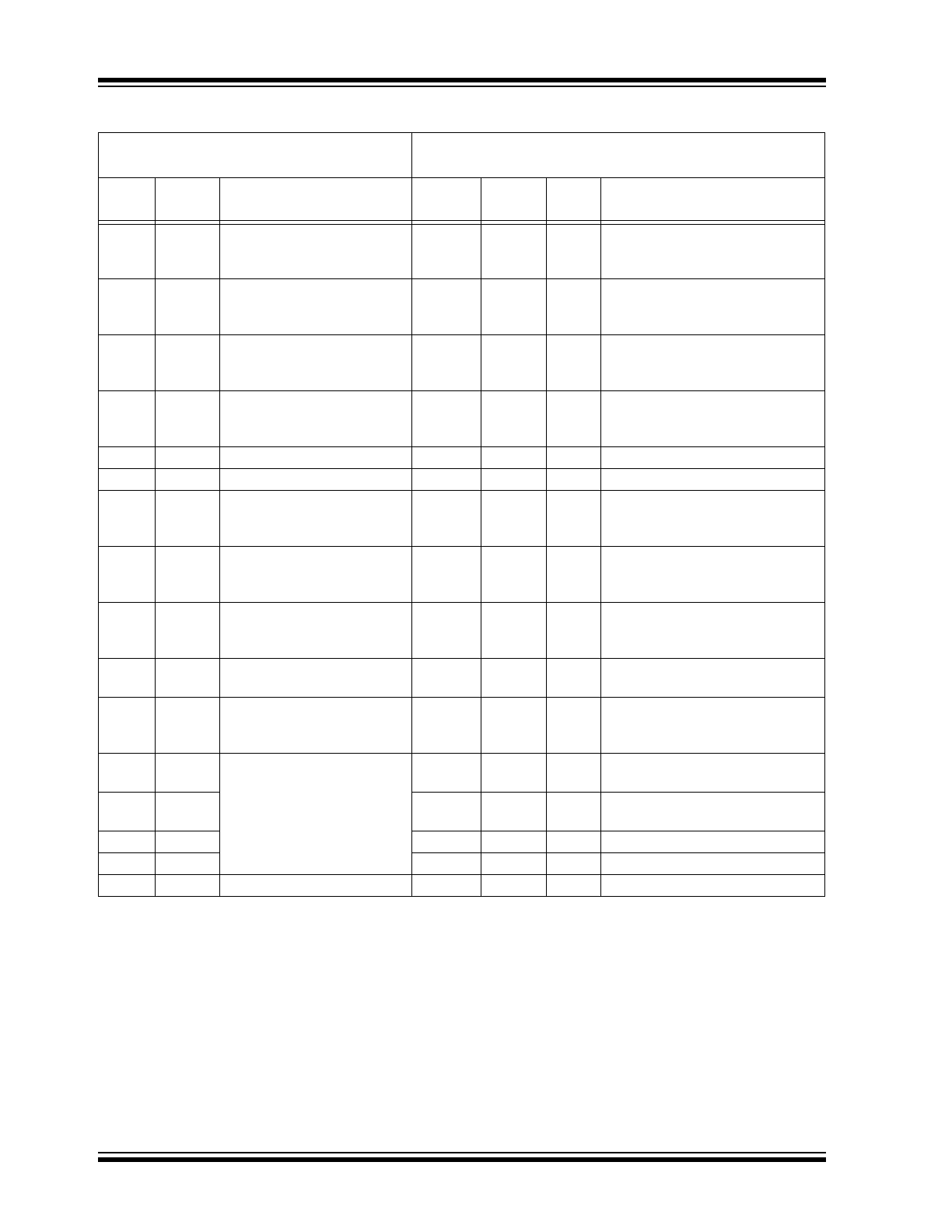
TABLE 1-2:
AC CHARACTERISTICS
All parameters apply over the specified
ranges unless otherwise noted.
Industrial (I):
T
A
= -40°C to +85°C, V
CC
= +1.8V to 5.5V
Automotive (E): T
A
= -40°C to +125°C, V
CC
= +2.5V to 5.5V
Param.
No.
Symbol
Parameter
Min.
Max.
Units
Conditions
A1
F
CLK
Clock frequency
—
3
2
1
MHz
MHz
MHz
4.5V
V
CC
< 5.5V
2.5V
V
CC
< 4.5V
1.8V
V
CC
< 2.5V
A2
T
CKH
Clock high time
200
250
450
—
ns
ns
ns
4.5V
V
CC
< 5.5V
2.5V
V
CC
< 4.5V
1.8V
V
CC
< 2.5V
A3
T
CKL
Clock low time
100
200
450
—
ns
ns
ns
4.5V
V
CC
< 5.5V
2.5V
V
CC
< 4.5V
1.8V
V
CC
< 2.5V
A4
T
CSS
Chip Select setup time
50
100
250
—
ns
ns
ns
4.5V
V
CC
< 5.5V
2.5V
V
CC
< 4.5V
1.8V
V
CC
< 2.5V
A5
T
CSH
Chip Select hold time
0
—
ns
1.8V
V
CC
< 5.5V
A6
T
CSL
Chip Select low time
250
—
ns
1.8V
V
CC
< 5.5V
A7
T
DIS
Data input setup time
50
100
250
—
ns
ns
ns
4.5V
V
CC
< 5.5V
2.5V
V
CC
< 4.5V
1.8V
V
CC
< 2.5V
A8
T
DIH
Data input hold time
50
100
250
—
ns
ns
ns
4.5V
V
CC
< 5.5V
2.5V
V
CC
< 4.5V
1.8V
V
CC
< 2.5V
A9
T
PD
Data output delay time
—
100
250
400
ns
ns
ns
4.5V
V
CC
< 5.5V, CL = 100 pF
2.5V
V
CC
< 4.5V, CL = 100 pF
1.8V
V
CC
< 2.5V, CL = 100 pF
A10
T
CZ
Data output disable time
—
100
200
ns
ns
4.5V
V
CC
< 5.5V, (Note 1)
1.8V
V
CC
< 4.5V, (Note 1)
A11
T
SV
Status valid time
—
200
300
500
ns
ns
ns
4.5V
V
CC
< 5.5V, CL = 100 pF
2.5V
V
CC
< 4.5V, CL = 100 pF
1.8V
V
CC
< 2.5V, CL = 100 pF
A12
T
WC
Program cycle time
—
5
ms
Erase/Write mode (AA and LC
versions)
A13
T
WC
—
2
ms
Erase/Write mode
(93C versions)
A14
T
EC
—
6
ms
ERAL mode, 4.5V
V
CC
5.5V
A15
T
WL
—
15
ms
WRAL mode, 4.5V
V
CC
5.5V
A16
—
Endurance
1M
—
cycles 25°C, V
CC
= 5.0V, (Note 2)
Note 1:
This parameter is periodically sampled and not 100% tested.
2:
This application is not tested but ensured by characterization. For endurance estimates in a specific
application, please consult the Total Endurance™ Model, which may be obtained from Microchip’s web
site at www.microchip.com.
2003-2012 Microchip Technology Inc.
DS21797L-page 5
93AA86A/B/C, 93LC86A/B/C, 93C86A/B/C
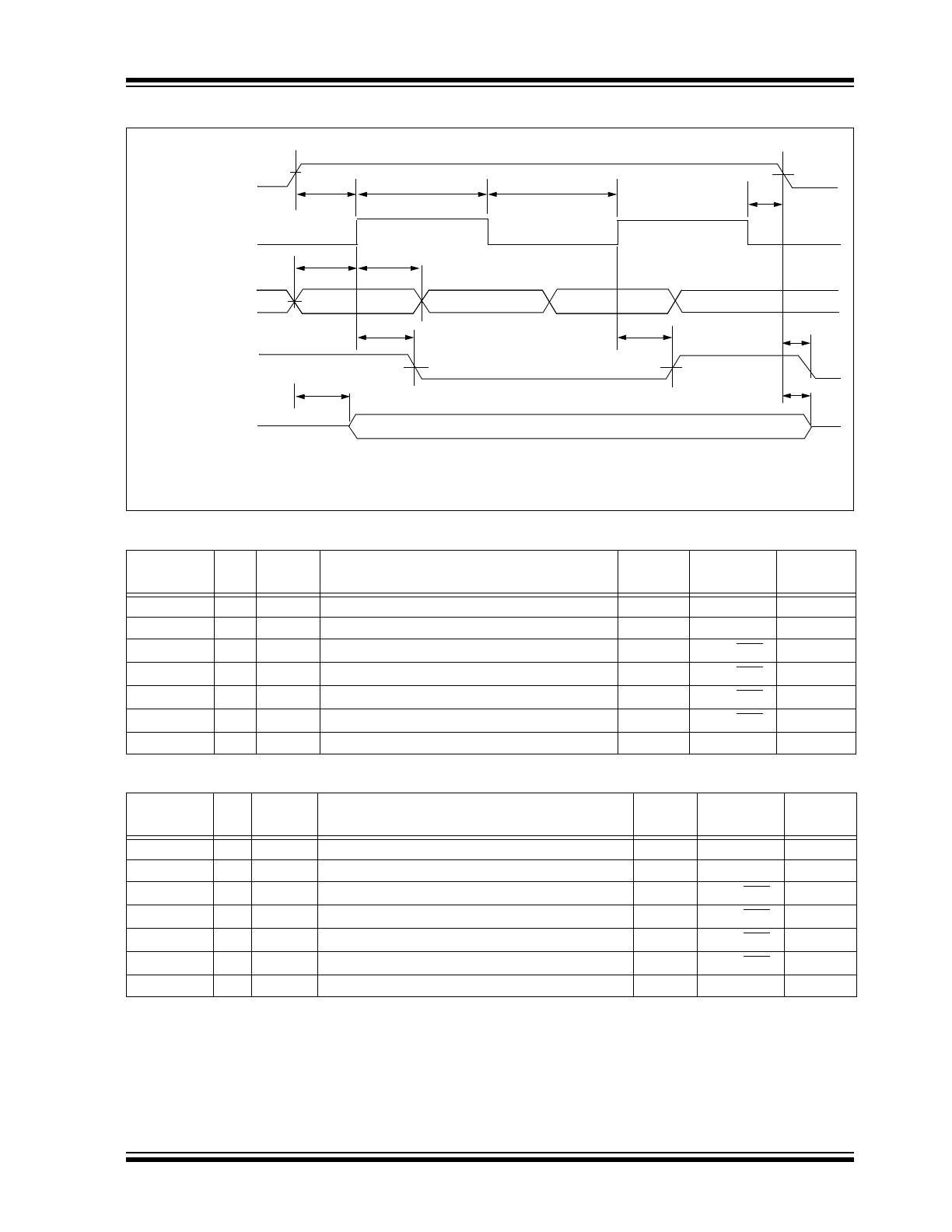
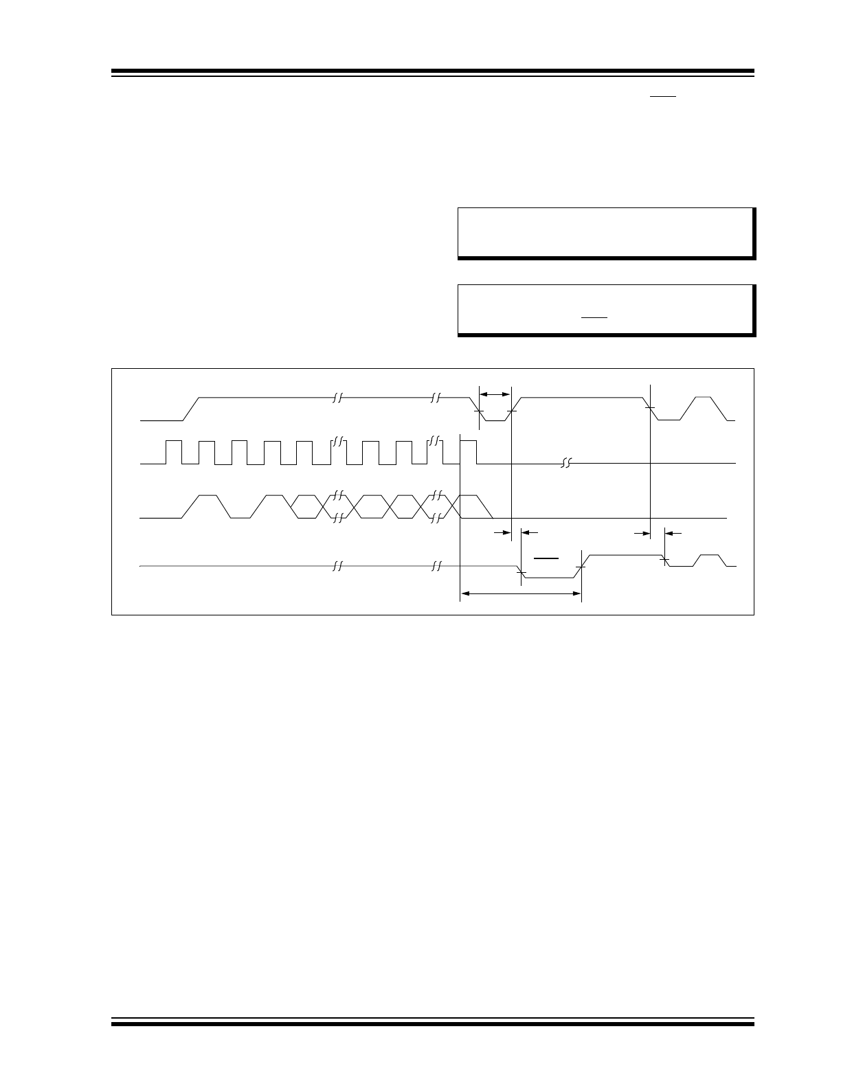
FIGURE 1-1:
SYNCHRONOUS DATA TIMING
TABLE 1-3:
INSTRUCTION SET FOR X16 ORGANIZATION (93XX86B OR 93XX86C WITH ORG = 1)
TABLE 1-4:
INSTRUCTION SET FOR X8 ORGANIZATION (93XX86A OR 93XX86C WITH ORG = 0)
Instruction
SB
Opcode
Address
Data In
Data Out
Req. CLK
Cycles
READ
1
10
A9 A8 A7 A6 A5 A4 A3 A2 A1 A0
—
D15-D0
29
EWEN
1
00
1
1
X
X
X
X
X
X
X
X
—
HighZ
13
ERASE
1
11
A9 A8 A7 A6 A5 A4 A3 A2 A1 A0
—
(RDY/
BSY
)
13
ERAL
1
00
1
0
X
X
X
X
X
X
X
X
—
(RDY/
BSY
)
13
WRITE
1
01
A9 A8 A7 A6 A5 A4 A3 A2 A1 A0
D15-D0
(RDY/
BSY
)
29
WRAL
1
00
0
1
X
X
X
X
X
X
X
X
D15-D0
(RDY/
BSY
)
29
EWDS
1
00
0
0
X
X
X
X
X
X
X
X
—
High-Z
13
Instruction
SB
Opcode
Address
Data In
Data Out
Req. CLK
Cycles
READ
1
10
A10 A9 A8 A7 A6 A5 A4 A3 A2 A1 A0
—
D7-D0
22
EWEN
1
00
1
1
X
X
X
X
X
X
X
X
X
—
High-Z
14
ERASE
1
11
A10 A9 A8 A7 A6 A5 A4 A3 A2 A1 A0
—
(RDY/
BSY
)
14
ERAL
1
00
1
0
X
X
X
X
X
X
X
X
X
—
(RDY/
BSY
)
14
WRITE
1
01
A10 A9 A8 A7 A6 A5 A4 A3 A2 A1 A0
D7-D0
(RDY/
BSY
)
22
WRAL
1
00
0
1
X
X
X
X
X
X
X
X
X
D7-D0
(RDY/
BSY
)
22
EWDS
1
00
0
0
X
X
X
X
X
X
X
X
X
—
High-Z
14
CS
V
IH
V
IL
V
IH
V
IL
V
IH
V
IL
V
OH
V
OL
V
OH
V
OL
CLK
DI
DO
(Read)
DO
(Program)
T
CSS
T
DIS
T
CKH
T
CKL
T
DIH
T
PD
T
CSH
T
PD
T
CZ
Status Valid
T
SV
T
CZ
Note: T
SV
is relative to CS.
93AA86A/B/C, 93LC86A/B/C, 93C86A/B/C
DS21797L-page 6
2003-2012 Microchip Technology Inc.
2.0
FUNCTIONAL DESCRIPTION
When the ORG pin (93XX86C) is connected to V
CC
,
the (x16) organization is selected. When it is connected
to ground, the (x8) organization is selected. Instruc-
tions, addresses and write data are clocked into the DI
pin on the rising edge of the clock (CLK). The DO pin is
normally held in a High-Z state except when reading
data from the device, or when checking the Ready/
Busy
status during a programming operation. The
Ready/
Busy
status can be verified during an Erase/
Write operation by polling the DO pin; DO low indicates
that programming is still in progress, while DO high
indicates the device is ready. DO will enter the High-Z
state on the falling edge of CS.
2.1
Start Condition
The Start bit is detected by the device if CS and DI are
both high with respect to the positive edge of CLK for
the first time.
Before a Start condition is detected, CS, CLK and DI
may change in any combination (except to that of a
Start condition), without resulting in any device
operation (Read, Write, Erase, EWEN, EWDS, ERAL
or WRAL). As soon as CS is high, the device is no
longer in Standby mode.
An instruction following a Start condition will only be
executed if the required opcode, address and data bits
for any particular instruction are clocked in.
2.2
Data In/Data Out (DI/DO)
It is possible to connect the Data In and Data Out pins
together. However, with this configuration it is possible
for a “bus conflict” to occur during the “dummy zero”
that precedes the read operation, if A0 is a logic high
level. Under such a condition the voltage level seen at
Data Out is undefined and will depend upon the relative
impedances of Data Out and the signal source driving
A0. The higher the current sourcing capability of the
driver, the higher the voltage at the Data Out pin. In
order to limit this current, a resistor should be
connected between DI and DO.
2.3
Data Protection
All modes of operation are inhibited when V
CC
is below
a typical voltage of 1.5V for ‘93AA’ and ‘93LC’ devices
or 3.8V for ‘93C’ devices.
The EWEN and EWDS commands give additional
protection against accidentally programming during
normal operation.
After power-up the device is automatically in the EWDS
mode. Therefore, an EWEN instruction must be
performed before the initial ERASE or WRITE instruction
can be executed.
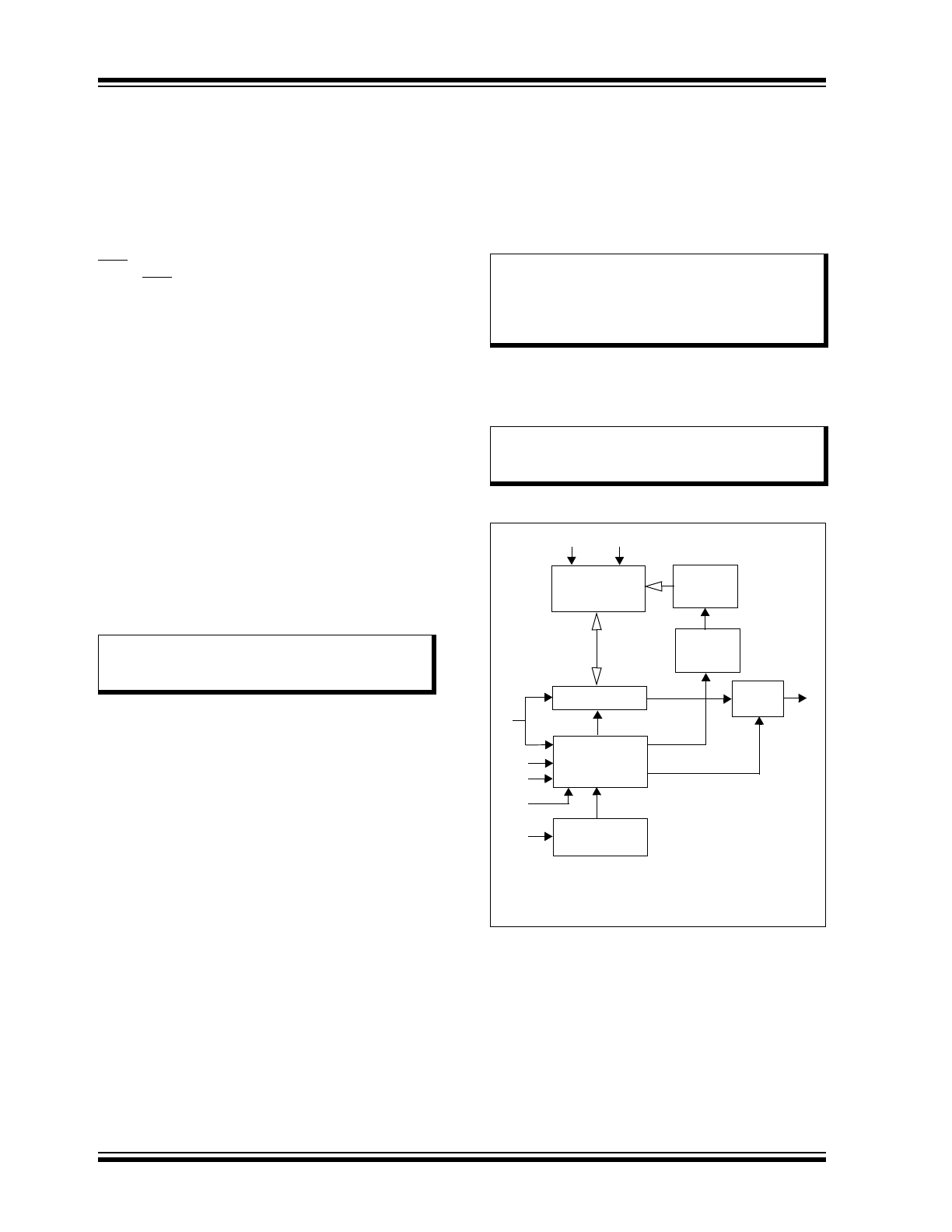
Block Diagram
Note:
When preparing to transmit an instruction,
either the CLK or DI signal levels must be
at a logic low as CS is toggled active high.
Note:
For added protection, an EWDS command
should be performed after every write
operation and an external 10 k
pull-
down protection resistor should be added
to the CS pin.
Note:
To prevent accidental writes to the array in
the 93XX86C devices, set the PE pin to a
logic low.
Memory
Array
Data Register
Mode
Decode
Logic
Clock
Register
Address
Decoder
Address
Counter
Output
Buffer
DO
DI
ORG*
CS
CLK
V
CC
V
SS
PE*
*ORG and PE inputs are not available on
A/B devices.
2003-2012 Microchip Technology Inc.
DS21797L-page 7
93AA86A/B/C, 93LC86A/B/C, 93C86A/B/C
2.4
Erase
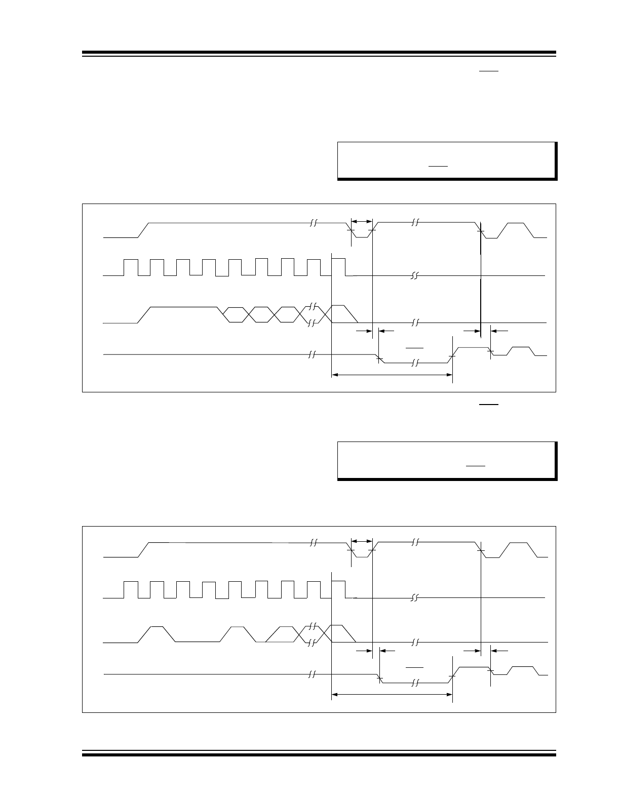
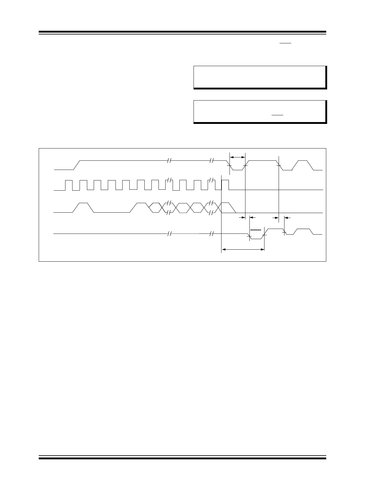
The ERASE instruction forces all data bits of the
specified address to the logical ‘1’ state. The rising
edge of CLK before the last address bit initiates the
write cycle.
The DO pin indicates the Ready/
Busy
status of the
device if CS is brought high after a minimum of 250 ns
low (T
CSL
). DO at logical ‘0’ indicates that programming
is still in progress. DO at logical ‘1’ indicates that the
register at the specified address has been erased and
the device is ready for another instruction.
FIGURE 2-1:
ERASE TIMING
2.5
Erase All (ERAL)
The Erase All (ERAL) instruction will erase the entire
memory array to the logical ‘1’ state. The ERAL cycle
is identical to the erase cycle, except for the different
opcode. The ERAL cycle is completely self-timed. The
rising edge of CLK before the last data bit initiates the
write cycle. Clocking of the CLK pin is not necessary
after the device has entered the ERAL cycle.
The DO pin indicates the Ready/
Busy
status of the
device, if CS is brought high after a minimum of 250 ns
low (T
CSL
).
V
CC
must be
4.5V for proper operation of ERAL.
FIGURE 2-2:
ERAL TIMING
Note:
After the Erase cycle is complete, issuing
a Start bit and then taking CS low will clear
the Ready/
Busy
status from DO.
CS
CLK
DI
DO
T
CSL
Check Status
1
1
1
A
N
A
N
-1
A
N
-2
•••
A0
T
SV
T
CZ
Busy
Ready
High-Z
T
WC
High-Z
Note:
After the ERAL command is complete,
issuing a Start bit and then taking CS low
will clear the Ready/
Busy
status from DO.
CS
CLK
DI
DO
T
CSL
Check Status
1
0
0
1
0
x
•••
x
T
SV
T
CZ
Busy
Ready
High-Z
T
EC
High-Z
93AA86A/B/C, 93LC86A/B/C, 93C86A/B/C
DS21797L-page 8
2003-2012 Microchip Technology Inc.
2.6
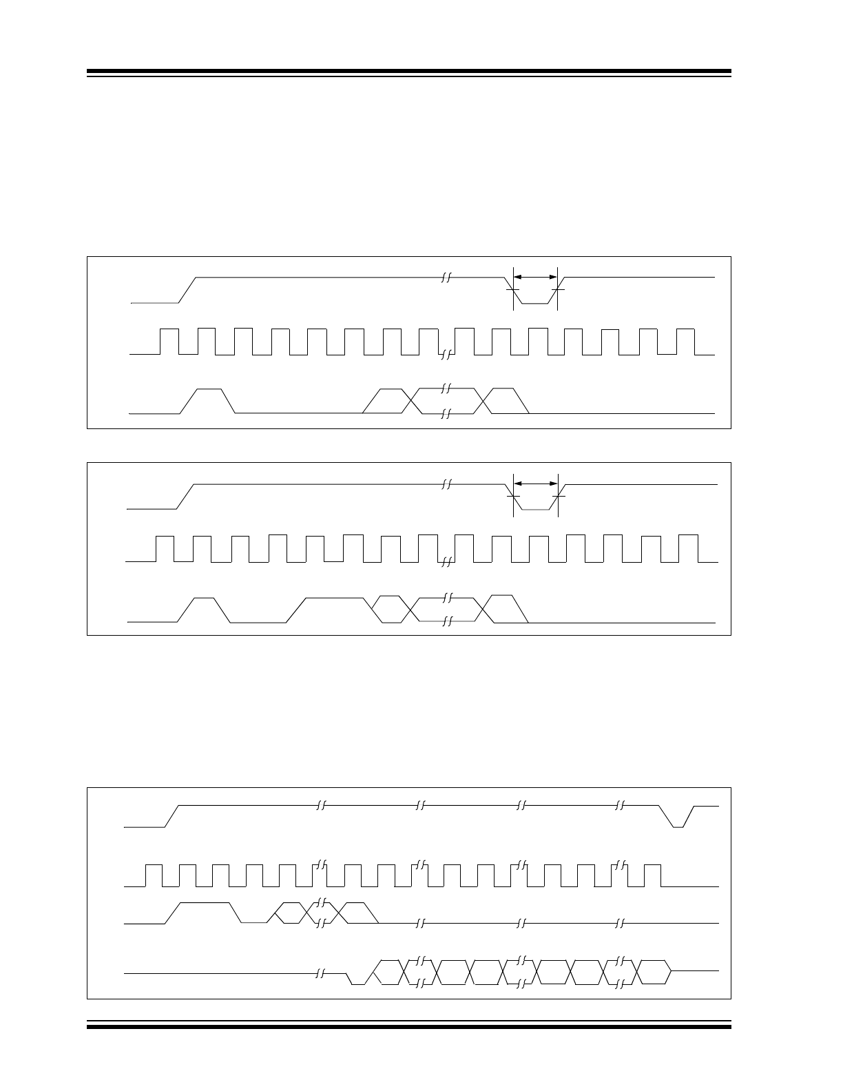
Erase/Write Disable and Enable
(EWDS/EWEN)
The 93XX86A/B/C powers up in the Erase/Write
Disable (EWDS) state. All programming modes must be
preceded by an Erase/Write Enable (EWEN) instruction.
Once the EWEN instruction is executed, programming
remains enabled until an EWDS instruction is executed
or V
CC
is removed from the device.
To protect against accidental data disturbance, the
EWDS
instruction can be used to disable all Erase/Write
functions and should follow all programming
operations. Execution of a READ instruction is
independent of both the EWEN and EWDS instructions.
FIGURE 2-3:
EWDS TIMING
FIGURE 2-4:
EWEN TIMING
2.7
Read
The READ instruction outputs the serial data of the
addressed memory location on the DO pin. A dummy
zero bit precedes the 8-bit (If ORG pin is low or A-Version
devices) or 16-bit (If ORG pin is high or B-version
devices) output string.
The output data bits will toggle on the rising edge of the
CLK and are stable after the specified time delay (T
PD
).
Sequential read is possible when CS is held high. The
memory data will automatically cycle to the next register
and output sequentially.
FIGURE 2-5:
READ TIMING
CS
CLK
DI
1
0
0
0
0
x
•••
x
T
CSL
1
x
CS
CLK
DI
0
0
1
1
x
T
CSL
•••
CS
CLK
DI
DO
1
1
0
A
N
•••
A0
High-Z
0
Dx
•••
D0
Dx
•••
D0
•••
Dx
D0
2003-2012 Microchip Technology Inc.
DS21797L-page 9
93AA86A/B/C, 93LC86A/B/C, 93C86A/B/C
2.8
Write
The WRITE instruction is followed by 8 bits (If ORG is
low or A-version devices) or 16 bits (If ORG pin is high
or B-version devices) of data which are written into the
specified address. The self-timed auto-erase and
programming cycle is initiated by the rising edge of CLK
on the last data bit.
The DO pin indicates the Ready/
Busy
status of the
device, if CS is brought high after a minimum of 250 ns
low (T
CSL
). DO at logical ‘0’ indicates that programming
is still in progress. DO at logical ‘1’ indicates that the
register at the specified address has been written with
the data specified and the device is ready for another
instruction.
FIGURE 2-6:
WRITE TIMING
Note:
The write sequence requires a logic high
signal on the PE pin prior to the rising
edge of the last data bit.
Note:
After the Write cycle is complete, issuing a
Start bit and then taking CS low will clear
the Ready/
Busy
status from DO
CS
CLK
DI
DO
1
0
1
A
N
•••
A0
Dx
•••
D0
Busy
Ready
High-Z
High-Z
T
WC
T
CSL
T
CZ
T
SV
93AA86A/B/C, 93LC86A/B/C, 93C86A/B/C
DS21797L-page 10
2003-2012 Microchip Technology Inc.
2.9
Write All (WRAL)
The Write All (WRAL) instruction will write the entire
memory array with the data specified in the command.
The self-timed auto-erase and programming cycle is
initiated by the rising edge of CLK on the last data bit.
Clocking of the CLK pin is not necessary after the
device has entered the WRAL cycle. The WRAL
command does include an automatic ERAL cycle for
the device. Therefore, the WRAL instruction does not
require an ERAL instruction, but the chip must be in the
EWEN status.
The DO pin indicates the Ready/
Busy
status of the
device if CS is brought high after a minimum of 250 ns
low (T
CSL
).
V
CC
must be
4.5V for proper operation of WRAL.
FIGURE 2-7:
WRAL TIMING
Note:
The write sequence requires a logic high
signal on the PE pin prior to the rising
edge of the last data bit.
Note:
After the Write All cycle is complete,
issuing a Start bit and then taking CS low
will clear the Ready/
Busy
status from DO.
CS
CLK
DI
DO
H
IGH
-Z
1
0
0
0
1
x
•••
x
Dx
•••
D0
High-Z
Busy
Ready
T
WL
T
CSL
T
SV
T
CZ