
2018 Microchip Technology Inc.
DS20005852A-page 1
MIC4604
Features
• 5.5V to 16V Gate Drive Supply Voltage Range
• Drives High-Side and Low-Side N-Channel
MOSFETs with Independent Inputs
• TTL Input Thresholds
• On-Chip Bootstrap Diode
• Fast 39 ns Propagation Times
• Drives 1000 pF Load with 20 ns Rise and Fall
Times
• Low Power Consumption
• Supplies Undervoltage Protection
• –40°C to +125°C Junction Temperature Range
Applications
• Power Inverters
• High Voltage Step-Down Regulators
• Half, Full, and 3-Phase Bridge Motor Drives
• Distributed Power Systems
• Computing Peripherals
General Description
The MIC4604 is an 85V Half-Bridge MOSFET driver.
The MIC4604 features fast 39 ns propagation delay
times and 20 ns driver rise/fall times for a 1 nF
capacitive load. The low-side and high-side gate
drivers are independently controlled. The MIC4604 has
TTL input thresholds. It includes a high-voltage internal
diode that helps charge the high-side gate drive
bootstrap capacitor.
A robust, high-speed, and low-power level shifter
provides clean level transitions to the high-side output.
The robust operation of the MIC4604 ensures that the
outputs are not affected by supply glitches, HS ringing
below ground, or HS slewing with high-speed voltage
transitions. Undervoltage protection is provided on both
the low-side and high-side drivers.
The MIC4604 is available in an 8-pin SOIC package
and a tiny 10-pin 2.5 mm x 2.5 mm TDFN package.
Both packages have an operating junction temperature
range of –40°C to +125°C.
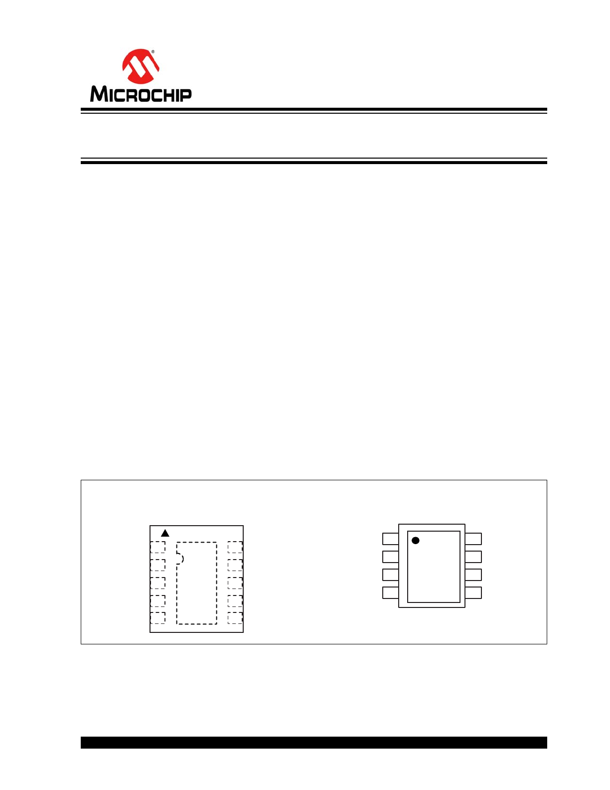
Package Types
MIC4604YMT
10-Pin TDFN (MT)
(Top View)
MIC4604YM
SOIC-8 (M)
(Top View)
EP
HS
HI
5
1
VDD
NC
HB
HO
10 NC
LO
VSS
LI
9
8
7
2
3
4
6
1
VDD
HB
HO
HS
8
LO
VSS
LI
HI
7
6
5
2
3
4
85V Half-Bridge MOSFET Driver with up to
16V Programmable Gate Drive
MIC4604
DS20005852A-page 2
2018 Microchip Technology Inc.
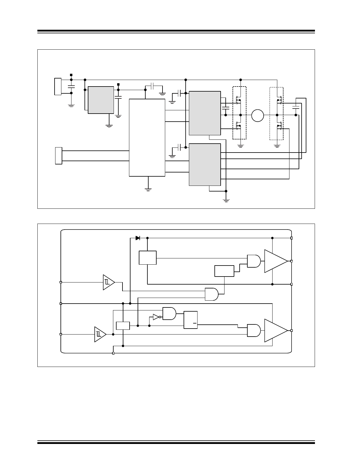
Typical Application Circuit
Motor Door Lock Solution
MIC4604
Half-Bridge
Driver
HI
LI
22μF
16V
M
22μF
16V
MIC4604
Half-Bridge
Driver
HB
HS
LO
HO
DC Motor
12V 140mA
μC
MAQ5283
LDO
12V to 5V
VDD
GND
EN
VOUT
VIN
1μF
16V
2.2μF
10V
22μF
16V
AQ4882
AQ4882
CAN BUS
12VDC
5.0V
0.1μF
10V
J1
Power
J2
Communication
VSS
VDD
CANL
CANH
22μF
16V
HI
LI
HB
HS
LO
HO
VDD
I/O
I/O
I/O
I/O
Functional Block Diagram
HB
HS
HO
LO
HI
LI
DRIVER
DRIVER
UVLO
LEVEL
SHIFT
VDD
R
Q
S
Q
VSS
HB
UVLO

2018 Microchip Technology Inc.
DS20005852A-page 3
MIC4604
1.0
ELECTRICAL CHARACTERISTICS
Absolute Maximum Ratings †
Supply Voltage (V
DD
, V
HB
– V
HS
) .............................................................................................................. –0.3V to +18V
Input Voltages (V
LI
, V
HI
, V
EN
) ...........................................................................................................–0.3V to V
DD
+ 0.3V
Voltage on LO (V
LO
)..........................................................................................................................–0.3V to V
DD
+ 0.3V
Voltage on HO (V
HO
).................................................................................................................V
HS
– 0.3V to V
HB
+ 0.3V
Voltage on HS (Continuous) ...................................................................................................................... –0.3V to +90V
Voltage on HB .........................................................................................................................................................+108V
Average Current in V
DD
to HB Diode ....................................................................................................................100 mA
ESD Rating (
Note 1
) ...................................................................................................................HBM: 1.5 kV; MM: 200V
Operating Ratings ‡
Supply Voltage (V
DD
) [Decreasing V
DD
] .................................................................................................. +5.25V to +16V
Supply Voltage (V
DD
) [Increasing V
DD
] ...................................................................................................... +5.5V to +16V
Voltage on HS ............................................................................................................................................ –0.3V to +85V
Voltage on HS (Repetitive Transient)......................................................................................................... –0.7V to +90V
HS Slew Rate........................................................................................................................................................ 50 V/ns
Voltage on HB ........................................................................................................................... V
HS
+ 4.5V to V
HS
+ 16V
and/or....................................................................................................................................... V
DD
– 1V to V
DD
+ 85V
†
Notice: Stresses above those listed under “Absolute Maximum Ratings” may cause permanent damage to the device.
This is a stress rating only and functional operation of the device at those or any other conditions above those indicated
in the operational sections of this specification is not intended. Exposure to maximum rating conditions for extended
periods may affect device reliability. Specifications are for packaged product only.
‡ Notice:
The device is not guaranteed to function outside its operating ratings.
Note 1:
Devices are ESD sensitive. Handling precautions are recommended. Human body model, 1.5 kΩ in series
with 100 pF.
MIC4604
DS20005852A-page 4
2018 Microchip Technology Inc.
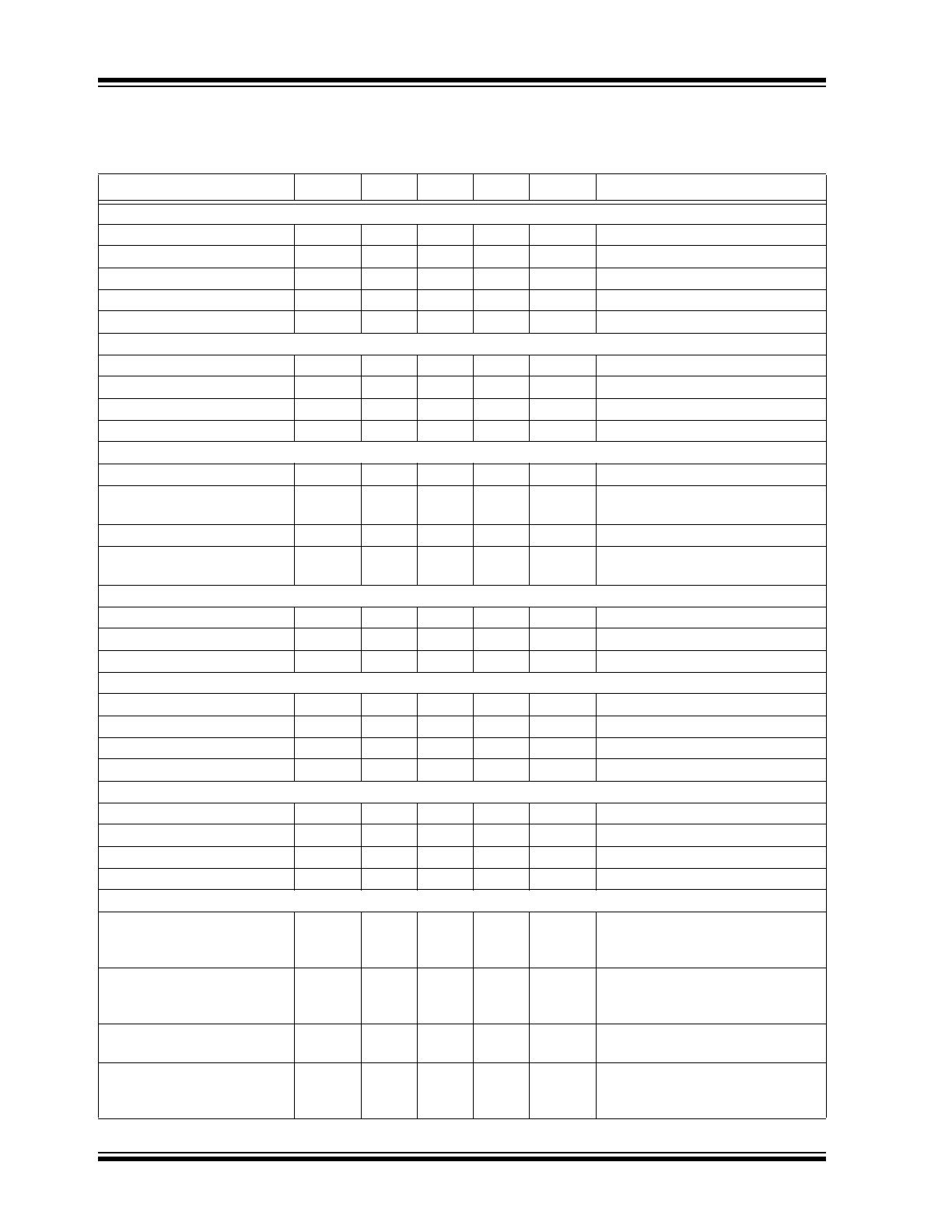
TABLE 1-1:
ELECTRICAL CHARACTERISTICS
Electrical Characteristics:
V
DD
= V
HB
= 12V; V
SS
= V
HS
= 0V; No load on LO or HO; T
A
= +25°C; unless otherwise
noted. Bold values indicate –40°C ≤ T
J
≤ +125°C.
Note 1
Parameter
Symbol
Min.
Typ.
Max.
Units
Conditions
Supply Current
V
DD
Quiescent Current
I
DD
—
48
200
µA
LI = HI = 0V
V
DD
Operating Current
I
DDO
—
136
300
µA
f = 20 kHz
Total HB Quiescent Current
I
HB
—
20
75
µA
LI = HI = 0V or LI = 0V and HI = 5V
Total HB Operating Current
I
HBO
—
29
200
µA
f = 20 kHz
HB to V
SS
Quiescent Current
I
HBS
—
0.5
5
µA
V
HS
= V
HB
= 90V
Input (LI, HI)
Low-Level Input Voltage
V
IL
—
—
0.8
V
—
High-Level Input Voltage
V
IH
2.2
—
—
V
—
Input Voltage Hysteresis
V
HYS
—
0.05
—
V
—
Input Pull-Down Resistance
R
I
100
240
500
kΩ
—
Undervoltage Protection
V
DD
Falling Threshold
V
DDF
4.0
4.4
4.9
V
—
V
DD
Threshold Hysteresis
V
DDH
—
0.21
—
V
Rising V
DD
Threshold; V
DDR
=
V
DDF
+ V
DDH
HB Falling Threshold
V
HBF
4.0
4.4
4.9
V
—
HB Threshold Hysteresis
V
HBH
—
0.23
—
V
Rising V
HB
Threshold; V
HBR
= V
HBF
+ V
HBH
Bootstrap Diode
Low-Current Forward Voltage
V
DL
—
0.42
0.70
V
I
VDD-HB
= 100 µA
High-Current Forward Voltage
V
DH
—
0.75
1.0
V
I
VDD-HB
= 50 mA
Dynamic Resistance
R
D
—
2.8
5.0
Ω
I
VDD-HB
= 50 mA
LO Gate Driver
Low-Level Output Voltage
V
OLL
—
0.17
0.4
V
I
LO
= 50 mA
High-Level Output Voltage
V
OHL
—
0.25
1.0
V
I
LO
= –50 mA, V
OHL
= V
DD
– V
LO
Peak Sink Current
I
OHL
—
1
—
A
V
LO
= 5V
Peak Source Current
I
OLL
—
1
—
A
V
LO
= 5V
HO Gate Driver
Low-Level Output Voltage
V
OLH
—
0.2
0.6
V
I
HO
= 50 mA
High-Level Output Voltage
V
OHH
—
0.22
1.0
V
I
HO
= –50 mA, V
OHH
= V
HB
– V
HO
Peak Sink Current
I
OHH
—
1.5
—
A
V
HO
= 5V
Peak Source Current
I
OLH
—
1
—
A
V
HO
= 5V
Switching Specifications
(
Note 2
)
Lower Turn-Off Propagation
Delay (LI Falling to LO
Falling)
t
LPHL
—
37
75
ns
—
Upper Turn-Off Propagation
Delay (HI Falling to HO
Falling)
t
HPHL
—
34
75
ns
—
Lower Turn-On Propagation
Delay (LI Rising to LO Rising)
t
LPLH
—
39
75
ns
—
Upper Turn-On Propagation
Delay (HI Rising to HO
Rising)
t
HPLH
—
33
75
ns
—
2018 Microchip Technology Inc.
DS20005852A-page 5
MIC4604
Output Rise/Fall Time
t
RC/FC
—
20
—
ns
C
L
= 1000 pF
Output Rise/Fall Time (3V to
9V)
t
R/F
—
0.8
—
µs
C
L
= 0.1 µF
Minimum Input Pulse Width
that Changes the Output
t
PW
—
50
—
ns
—
Bootstrap Diode Turn-On or
Turn-Off Time
t
BS
—
10
—
ns
—
Note 1:
Specifications are for packaged product only.
2:
Guaranteed by design. Not production tested.
TABLE 1-1:
ELECTRICAL CHARACTERISTICS (CONTINUED)
Electrical Characteristics:
V
DD
= V
HB
= 12V; V
SS
= V
HS
= 0V; No load on LO or HO; T
A
= +25°C; unless otherwise
noted. Bold values indicate –40°C ≤ T
J
≤ +125°C.
Note 1
Parameter
Symbol
Min.
Typ.
Max.
Units
Conditions
TEMPERATURE SPECIFICATIONS (
Note 1
)
Parameters
Sym.
Min.
Typ.
Max.
Units
Conditions
Temperature Ranges
Junction Operating Temperature
Range
T
J
–40
—
+125
°C
—
Storage Temperature Range
T
S
–60
—
+150
°C
—
Package Thermal Resistances
Thermal Resistance TDFN-10Ld
JA
—
75
—
°C/W
—
Thermal Resistance SOIC-8
JA
—
98.9
—
°C/W
—
Note 1:
The maximum allowable power dissipation is a function of ambient temperature, the maximum allowable
junction temperature and the thermal resistance from junction to air (i.e., T
A
, T
J
,
JA
). Exceeding the
maximum allowable power dissipation will cause the device operating junction temperature to exceed the
maximum +125°C rating. Sustained junction temperatures above +125°C can impact the device reliability.
MIC4604
DS20005852A-page 6
2018 Microchip Technology Inc.
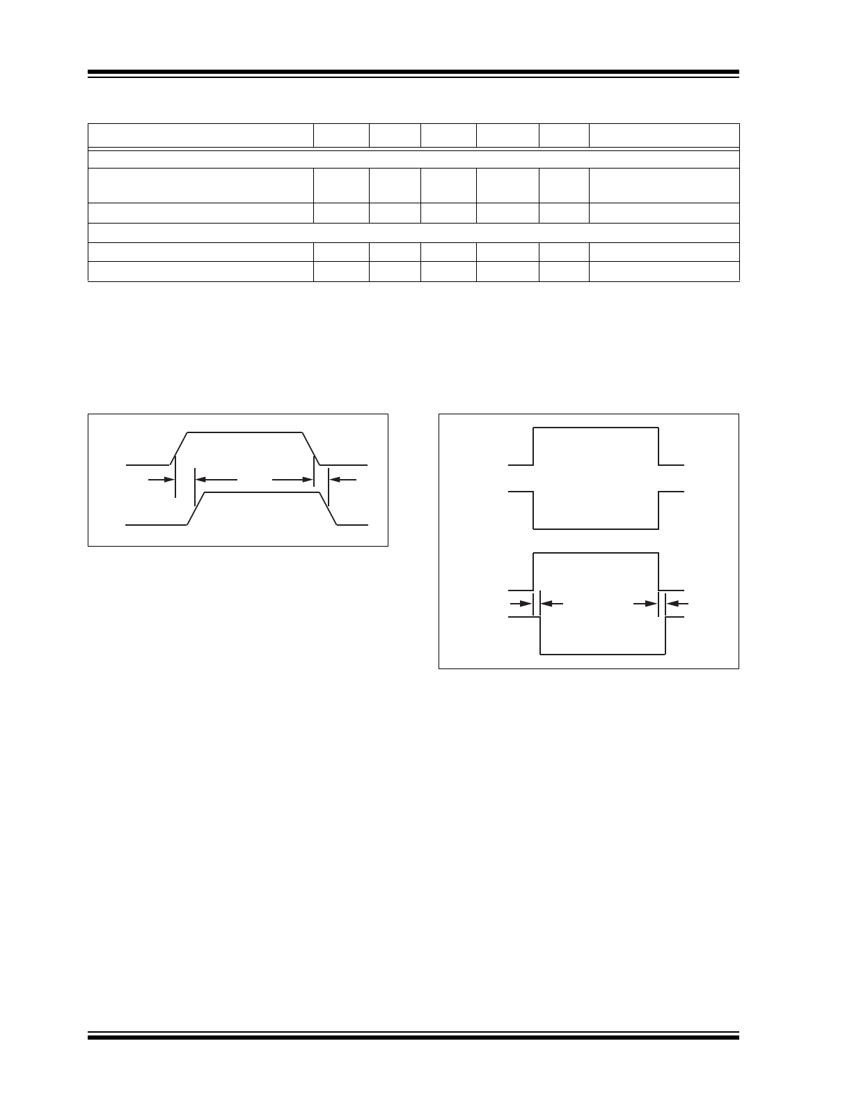
Timing Diagrams
t
HPLH
t
LPLH
t
HPLH
t
LPLH
HI, LI
HO, LO
Note 1:
All propagation delays are measured from
the 50% voltage level.
LI
LO
HI
HO
t
MON
t
MOFF
2018 Microchip Technology Inc.
DS20005852A-page 7
MIC4604
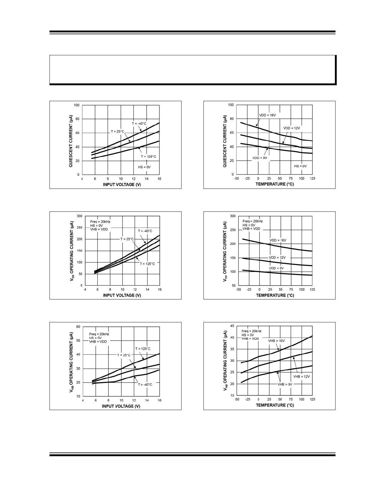
2.0
TYPICAL PERFORMANCE CURVES
Note:
The graphs and tables provided following this note are a statistical summary based on a limited number of
samples and are provided for informational purposes only. The performance characteristics listed herein
are not tested or guaranteed. In some graphs or tables, the data presented may be outside the specified
operating range (e.g., outside specified power supply range) and therefore outside the warranted range.
FIGURE 2-1:
Quiescent Current vs. Input
Voltage.
FIGURE 2-2:
V
DD
Operating Current vs.
Input Voltage.
FIGURE 2-3:
V
HB
Operating Current vs.
Input Voltage.
FIGURE 2-4:
Quiescent Current vs. Input
Temperature.
FIGURE 2-5:
V
DD
Operating Current vs.
Temperature.
FIGURE 2-6:
V
HB
Operating Current vs.
Temperature.
MIC4604
DS20005852A-page 8
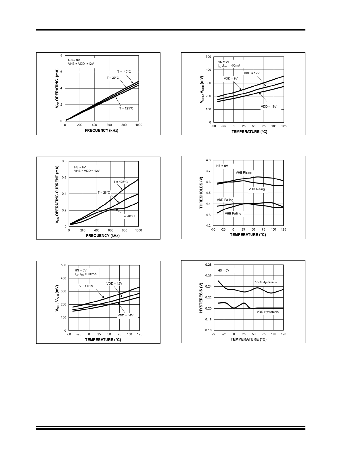
2018 Microchip Technology Inc.
FIGURE 2-7:
V
DD
Operating Current vs.
Frequency.
FIGURE 2-8:
V
HB
Operating Current vs.
Frequency.
FIGURE 2-9:
Low Level Output Voltage
vs. Temperature.
FIGURE 2-10:
High Level Output Voltage
vs. Temperature.
FIGURE 2-11:
UVLO Thresholds vs.
Temperature.
FIGURE 2-12:
UVLO Hysteresis vs.
Temperature.
2018 Microchip Technology Inc.
DS20005852A-page 9
MIC4604
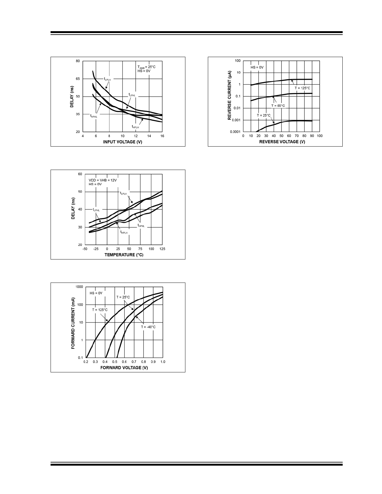
FIGURE 2-13:
Propagation Delay vs. Input
Voltage.
FIGURE 2-14:
Propagation Delay vs.
Temperature.
FIGURE 2-15:
Bootstrap Diode I-V
Characteristics.
FIGURE 2-16:
Bootstrap Diode Reverse
Current.

MIC4604
DS20005852A-page 10
2018 Microchip Technology Inc.
3.0
PIN DESCRIPTIONS
The descriptions of the pins are listed in
Table 3-1
.
TABLE 3-1:
PIN FUNCTION TABLE
Pin Number
TDFN
Pin Number
SOIC
Pin Name
Description
1
1
VDD
Input supply for gate drivers. Decouple this pin to V
SS
with a >2.2 µF
capacitor. Anode connection to internal bootstrap diode.
2, 10
—
NC
No connect.
3
2
HB
High-side bootstrap supply. External bootstrap capacitor is required.
Connect bootstrap capacitor across this pin and HS. Cathode
connection to internal bootstrap diode.
4
3
HO
High-side drive output. Connect to gate of the external high-side power
MOSFET.
5
4
HS
High-side drive reference connection. Connect to source of the external
high-side power MOSFET. Connect this pin to the bootstrap capacitor.
6
5
HI
High-side drive input.
7
6
LI
Low-side drive input.
8
7
VSS
Driver reference supply input. Connected to power ground of external
circuitry and to source of low-side power MOSFET.
9
8
LO
Low-side drive output. Connect to gate of the external low-side power
MOSFET.
EP
—
ePAD
Exposed pad. Connect to V
SS
.