

8371AS–AVR–08/12
Features
z
High Performance, Low Power Atmel
®
AVR
®
8-bit Microcontroller
z
Advanced RISC Architecture
z
123 Powerful Instructions – Most Single Clock Cycle Execution
z
32 x 8 General Purpose Working Registers
z
Fully Static Operation
z
Up to 20 MIPS Throughput at 20 MHz
z
Non-volatile Program and Data Memories
z
8K Bytes of In-System Programmable Flash Program Memory
z
Endurance: 10,000 Write/Erase Cycles
z
256 Bytes of In-System Programmable EEPROM
z
Endurance: 100,000 Write/Erase Cycles
z
512 Bytes Internal SRAM
z
Optional Boot Code Section with Independent Lock Bits
z
Data Retention: 20 Years at 85
o
C / 100 Years at 25
o
C
z
Peripheral Features
z
One 8-bit and one 16-bit Timer/Counter with Two PWM Channels, Each
z
Programmable Ultra Low Power Watchdog Timer
z
On-chip Analog Comparator
z
10-bit Analog to Digital Converter
z
28 External and 4 Internal, Single-ended Input Channels
z
Full Duplex USART with Start Frame Detection
z
Master/Slave SPI Serial Interface
z
Slave I
2
C Serial Interface
z
Special Microcontroller Features
z
Low Power Idle, ADC Noise Reduction, and Power-down Modes
z
Enhanced Power-on Reset Circuit
z
Programmable Brown-out Detection Circuit with Supply Voltage Sampling
z
External and Internal Interrupt Sources
z
Pin Change Interrupt on 28 Pins
z
Calibrated 8MHz Oscillator with Temperature Calibration Option
z
Calibrated 32kHz Ultra Low Power Oscillator
z
High-Current Drive Capability on 8 I/O Pins
z
I/O and Packages
z
32-lead TQFP, and 32-pad QFN/MLF: 28 Programmable I/O Lines
z
Speed Grade
z
0 – 2 MHz @ 1.7 – 1.8V
z
0 – 4 MHz @ 1.8 – 5.5V
z
0 – 10 MHz @ 2.7 – 5.5V
z
0 – 20 MHz @ 4.5 – 5.5V
ATtiny828
8-bit AVR Microcontroller with 8K Bytes In-System
Programmable Flash
DATASHEET SUMMARY
2
ATtiny828 [DATASHEET]
8371AS–AVR–08/12
z
Low Power Consumption
z
Active Mode: 0.2 mA at 1.8V and 1MHz
z
Idle Mode: 30 µA at 1.8V and 1MHz
z
Power-Down Mode (WDT Enabled): 1 µA at 1.8V
z
Power-Down Mode (WDT Disabled): 100 nA at 1.8V
1.
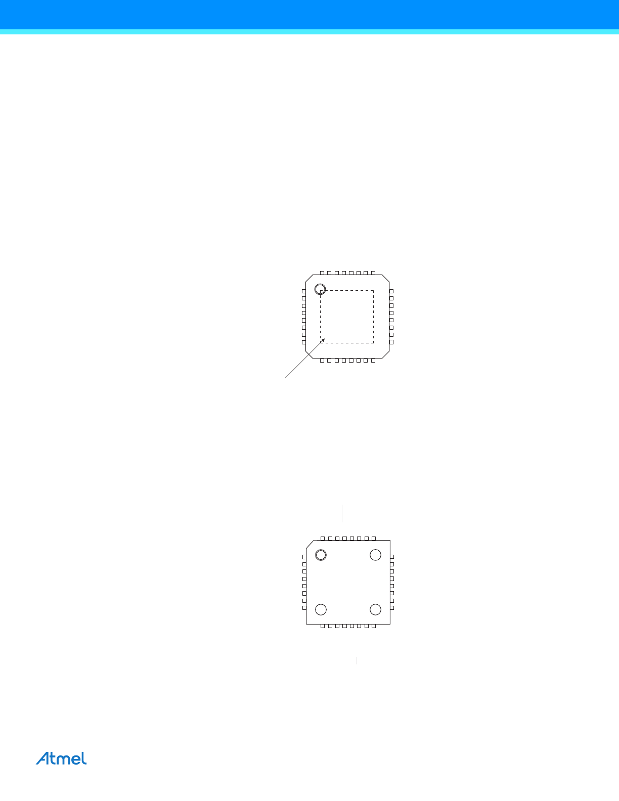
Pin Configurations
Figure 1.
ATtiny828 Pinout in MLF32.
Figure 2.
ATtiny828 Pinout in TQFP32.
1
2
3
4
5
6
7
8
24
23
22
21
20
19
18
17
32
31
30
29
28
27
26
25
9
10
11
12
13
14
15
16
(PCINT18/ADC18/TOCC2/RXD/INT1) PC2
(PCINT19/ADC19/TOCC3/TXD) PC3
(PCINT20/ADC20/TOCC4) PC4
VCC
GND
(PCINT21/ADC21/TOCC5/ICP1/T0) PC5
(PCINT22/ADC22/CLKI/TOCC6) PC6
(PCINT23/ADC23/TOCC7/T1) PC7
PB5 (PCINT13/ADC13)
PB4 (PCINT12/ADC12)
PB3 (PCINT11/ADC11)
GND
PB2 (PCINT10/ADC10)
PB1 (PCINT9/ADC9)
AVCC
PB0 (PCINT8/ADC8)
(P
CI
N
T
0
/A
D
C0
) P
A
0
(PC
IN
T
1
/A
D
C
1
/A
IN
0
) P
A
1
(PC
IN
T
2
/A
D
C
2
/A
IN
1
) P
A
2
(P
CI
N
T
3
/A
D
C3
) P
A
3
(P
CI
N
T
4
/A
D
C4
) P
A
4
(P
CI
N
T
5
/A
D
C5
) P
A
5
(P
CI
N
T
6
/A
D
C6
) P
A
6
(P
CI
N
T
7
/A
D
C7
) P
A
7
P
C
1 (
P
C
IN
T
17/
A
D
C
17/
T
O
C
C
1/
IN
T
0
/C
L
K
O)
P
C
0 (
P
C
IN
T
16/
A
D
C
16/
T
O
C
C
0/
S
S
/X
C
K
)
P
D
3 (
P
C
IN
T
27/
A
D
C
27/
S
C
L
/S
C
K
)
P
D
2 (
P
C
IN
T
26/
A
D
C
26/
R
E
S
E
T
/D
W
)
P
D
1 (
P
C
IN
T
25/
A
D
C
25/
M
IS
O
)
P
D
0 (
P
C
IN
T
24/
A
D
C
24/
S
D
A
/M
O
S
I)
P
B
7 (
P
C
IN
T
15/
A
D
C
15)
P
B
6 (
P
C
IN
T
14/
A
D
C
14)
NOTE: Bottom pad should be
soldered to ground
1
2
3
4
5
6
7
8
24
23
22
21
20
19
18
17
32
31
30
29
28
27
26
25
9
10
11
12
13
14
15
16
P
C
1 (
P
C
IN
T
17/
A
D
C
17/
T
O
C
C
1/
IN
T
0
/C
L
K
O
)
P
C
0 (
P
C
IN
T
16/
A
D
C
16/
T
O
C
C
0/
S
S
/X
C
K
)
P
D
3 (
P
C
IN
T
27/
A
D
C
27/
S
C
L
/S
C
K
)
P
D
2 (
P
C
IN
T
26/
A
D
C
26/
R
E
S
E
T
/D
W
)
P
D
1 (
P
C
IN
T
25/
A
D
C
25/
M
IS
O
)
P
D
0 (
P
C
IN
T
24/
A
D
C
24/
S
D
A
/M
O
S
I)
P
B
7 (
P
C
IN
T
15/
A
D
C
15)
P
B
6 (
P
C
IN
T
14/
A
D
C
14)
PB5 (PCINT13/ADC13)
PB4 (PCINT12/ADC12)
PB3 (PCINT11/ADC11)
GND
PB2 (PCINT10/ADC10)
PB1 (PCINT9/ADC9)
AVCC
PB0 (PCINT8/ADC8)
(P
CI
N
T
0
/A
D
C0
) P
A
0
(P
CI
N
T
1
/A
D
C1
/A
IN
0
) P
A
1
(P
CI
N
T
2
/A
D
C2
/A
IN
1
) P
A
2
(P
CI
N
T
3
/A
D
C3
) P
A
3
(P
CI
N
T
4
/A
D
C4
) P
A
4
(P
CI
N
T
5
/A
D
C5
) P
A
5
(P
CI
N
T
6
/A
D
C6
) P
A
6
(P
CI
N
T
7
/A
D
C7
) P
A
7
(PCINT18/ADC18/TOCC2/RXD/INT1) PC2
(PCINT19/ADC19/TOCC3/TXD) PC3
(PCINT20/ADC20/TOCC4) PC4
VCC
GND
(PCINT21/ADC21/TOCC5/ICP1/T0) PC5
(PCINT22/ADC22/CLKI/TOCC6) PC6
(PCINT23/ADC23/TOCC7/T1) PC7

3
ATtiny828 [DATASHEET]
8371AS–AVR–08/12
1.1
Pin Description
1.1.1
VCC
Supply voltage.
1.1.2
AVCC
AV
CC
is the supply voltage pin for the A/D converter and a selection of I/O pins. This pin should be externally connected
to V
CC
even if the ADC is not used. If the ADC is used, it is recommended this pin is connected to V
CC
through a low-pass
filter, as described in
“Noise Canceling Techniques” on page 145
.
All pins of Port A and Port B are powered by AV
CC
. All other I/O pins take their supply voltage from V
CC
.
1.1.3
GND
Ground.
1.1.4
RESET
Reset input. A low level on this pin for longer than the minimum pulse length will generate a reset, even if the clock is not
running and provided the reset pin has not been disabled. The minimum pulse length is given in
Table 107 on page 250
.
Shorter pulses are not guaranteed to generate a reset.
The reset pin can also be used as a (weak) I/O pin.
1.1.5
Port A (PA7:PA0)
This is an 8-bit, bi-directional I/O port with internal pull-up resistors (selected for each bit). Output buffers have high sink
and standard source capability. See
Table 107 on page 250
for port drive strength.
As inputs, port pins that are externally pulled low will source current provided that pull-up resistors are activated. Port
pins are tri-stated when a reset condition becomes active, even if the clock is not running.
This port has alternative pin functions for pin change interrupts, the analog comparator, and ADC. See
“Alternative Port
Functions” on page 63
.
1.1.6
Port B (PB7:PB0)
This is an 8-bit, bi-directional I/O port with internal pull-up resistors (selected for each bit). Output buffers have high sink
and standard source capability. See
Table 103 on page 247
for port drive strength.
As inputs, port pins that are externally pulled low will source current provided that pull-up resistors are activated. Port
pins are tri-stated when a reset condition becomes active, even if the clock is not running.
This port has alternative pin functions for pin change interrupts, and ADC. See
“Alternative Port Functions” on page 63
.
1.1.7
Port C (PC7:PC0)
This is an 8-bit, bi-directional I/O port with internal pull-up resistors (selected for each bit). Output buffers have high sink
and standard source capability. Optionally, extra high sink capability can be enabled. See
Table 103 on page 247
for port
drive strength.
As inputs, port pins that are externally pulled low will source current provided that pull-up resistors are activated. Port
pins are tri-stated when a reset condition becomes active, even if the clock is not running.
This port has alternative pin functions for pin change interrupts, ADC, timer/counter, external interrupts, and serial
interfaces. See
“Alternative Port Functions” on page 63
.
1.1.8
Port D (PD3:PD0)
This is a 4-bit, bi-directional I/O port with internal pull-up resistors (selected for each bit). Output buffers of PD0 and PD3
have symmetrical drive characteristics, with both sink and source capability. Output buffer PD1 has high sink and

4
ATtiny828 [DATASHEET]
8371AS–AVR–08/12
standard source capability, while PD2 only has weak drive characteristics due to its use as a reset pin. See
Table 103 on
page 247
for port drive strength.
As inputs, port pins that are externally pulled low will source current provided that pull-up resistors are activated. Port
pins are tri-stated when a reset condition becomes active, even if the clock is not running.
This port has alternative pin functions for pin change interrupts, ADC, serial interfaces, and debugWire. See
“Alternative
Port Functions” on page 63
.
5
ATtiny828 [DATASHEET]
8371AS–AVR–08/12
2.
Overview
ATtiny828 is a low-power CMOS 8-bit microcontrollers based on the AVR enhanced RISC architecture. By executing
powerful instructions in a single clock cycle, the ATtiny828 achieves throughputs approaching 1 MIPS per MHz allowing
the system designer to optimize power consumption versus processing speed.
Figure 3.
Block Diagram
The AVR core combines a rich instruction set with 32 general purpose working registers. All 32 registers are directly
connected to the Arithmetic Logic Unit (ALU), allowing two independent registers to be accessed in a single instruction,
executed in one clock cycle. The resulting architecture is compact and code efficient while achieving throughputs up to
ten times faster than conventional CISC microcontrollers.
DEBUG
INTERFACE
CALIBRATED ULP
OSCILLATOR
WATCHDOG
TIMER
CALIBRATED
OSCILLATOR
TIMING AND
CONTROL
V
CC
RESET
GND
8-BIT DATA BUS
PD[3:0]
CPU CORE
PROGRAM
MEMORY
(FLASH)
DATA
MEMORY
(SRAM)
POWER
SUPERVISION:
POR
BOD
RESET
ISP
INTERFACE
PORT A
PORT B
PORT C
PORT D
VOLTAGE
REFERENCE
MULTIPLEXER
ANALOG
COMPARATOR
ADC
TEMPERATURE
SENSOR
8-BIT
TIMER/COUNTER
16-BIT
TIMER/COUNTER
TWO-WIRE
INTERFACE
USART
EEPROM
ON-CHIP
DEBUGGER
PC[7:0]
PB[7:0]
PA[7:0]

6
ATtiny828 [DATASHEET]
8371AS–AVR–08/12
ATtiny828 provides the following features:
z
8K bytes of in-system programmable Flash
z
512 bytes of SRAM data memory
z
256 bytes of EEPROM data memory
z
28 general purpose I/O lines
z
32 general purpose working registers
z
An 8-bit timer/counter with two PWM channels
z
A16-bit timer/counter with two PWM channels
z
Internal and external interrupts
z
A 10-bit ADC with 4 internal and 28 external chanels
z
An ultra-low power, programmable watchdog timer with internal oscillator
z
A programmable USART with start frame detection
z
A slave, I
2
C compliant Two-Wire Interface (TWI)
z
A master/slave Serial Peripheral Interface (SPI)
z
A calibrated 8MHz oscillator
z
A calibrated 32kHz, ultra low power oscillator
z
Three software selectable power saving modes.
The device includes the following modes for saving power:
z
Idle mode: stops the CPU while allowing the timer/counter, ADC, analog comparator, SPI, TWI, and interrupt
system to continue functioning
z
ADC Noise Reduction mode: minimizes switching noise during ADC conversions by stopping the CPU and all I/O
modules except the ADC
z
Power-down mode: registers keep their contents and all chip functions are disabled until the next interrupt or
hardware reset
The device is manufactured using Atmel’s high density non-volatile memory technology. The Flash program memory can
be re-programmed in-system through a serial interface, by a conventional non-volatile memory programmer or by an on-
chip boot code, running on the AVR core. The boot program can use any interface to download the application program
to the Flash memory. Software in the boot section of the Flash executes while the application section of the Flash is
updated, providing true read-while-write operation.
The ATtiny828 AVR is supported by a full suite of program and system development tools including: C compilers, macro
assemblers, program debugger/simulators and evaluation kits.

7
ATtiny828 [DATASHEET]
8371AS–AVR–08/12
3.
General Information
3.1
Resources
A comprehensive set of drivers, application notes, data sheets and descriptions on development tools are available for
download at http://www.atmel.com/avr.
3.2
Code Examples
This documentation contains simple code examples that briefly show how to use various parts of the device. These code
examples assume that the part specific header file is included before compilation. Be aware that not all C compiler
vendors include bit definitions in the header files and interrupt handling in C is compiler dependent. Please confirm with
the C compiler documentation for more details.
3.3
Data Retention
Reliability Qualification results show that the projected data retention failure rate is much less than 1 PPM over 20 years
at 85°C or 100 years at 25°C.
8
ATtiny828 [DATASHEET]
8371AS–AVR–08/12
4.
Register Summary
Address
Name
Bit 7
Bit 6
Bit 5
Bit 4
Bit 3
Bit 2
Bit 1
Bit 0
Page(s)
(0xFF)
Reserved
–
–
–
–
–
–
–
–
(0xFE)
Reserved
–
–
–
–
–
–
–
–
(0xFD)
Reserved
–
–
–
–
–
–
–
–
(0xFC)
Reserved
–
–
–
–
–
–
–
–
(0xFB)
Reserved
–
–
–
–
–
–
–
–
(0xFA)
Reserved
–
–
–
–
–
–
–
–
(0xF9)
Reserved
–
–
–
–
–
–
–
–
(0xF8)
Reserved
–
–
–
–
–
–
–
–
(0xF7)
Reserved
–
–
–
–
–
–
–
–
(0xF6)
Reserved
–
–
–
–
–
–
–
–
(0xF5)
Reserved
–
–
–
–
–
–
–
–
(0xF4)
Reserved
–
–
–
–
–
–
–
–
(0xF3)
Reserved
–
–
–
–
–
–
–
–
(0xF2)
Reserved
–
–
–
–
–
–
–
–
(0xF1)
OSCTCAL0B
Oscillator Temperature Compensation Register B
Page
33
(0xF0)
OSCTCAL0A
Oscillator Temperature Compensation Register A
Page
33
(0xEF)
Reserved
–
–
–
–
–
–
–
–
(0xEE)
Reserved
–
–
–
–
–
–
–
–
(0xED)
Reserved
–
–
–
–
–
–
–
–
(0xEC)
Reserved
–
–
–
–
–
–
–
–
(0xEB)
Reserved
–
–
–
–
–
–
–
–
(0xEA)
Reserved
–
–
–
–
–
–
–
–
(0xE9)
TOCPMSA1
TOCC7S1
TOCC7S0
TOCC6S1
TOCC6S0
TOCC5S1
TOCC5S0
TOCC4S1
TOCC4S0
Page
127
(0xE8)
TOCPMSA0
TOCC3S1
TOCC3S0
TOCC2S1
TOCC2S0
TOCC1S1
TOCC1S0
TOCC0S1
TOCC0S0
Page
127
(0xE7)
Reserved
–
–
–
–
–
–
–
–
(0xE6)
Reserved
–
–
–
–
–
–
–
–
(0xE5)
Reserved
–
–
–
–
–
–
–
–
(0xE4)
Reserved
–
–
–
–
–
–
–
–
(0xE3)
Reserved
–
–
–
–
–
–
–
–
(0xE2)
TOCPMCOE
TOCC7OE
TOCC6OE
TOCC5OE
TOCC4OE
TOCC3OE
TOCC2OE
TOCC1OE
TOCC0OE
Page
128
(0xE1)
Reserved
–
–
–
–
–
–
–
–
(0xE0)
Reserved
–
–
–
–
–
–
–
–
(0xDF)
DIDR3
–
–
–
–
ADC27D
ADC26D
ADC25D
ADC24D
Page
154
(0xDE)
DIDR2
ADC23D
ADC22D
ADC21D
ADC20D
ADC19D
ADC18D
ADC17D
ADC16D
Page
154
(0xDD)
Reserved
–
–
–
–
–
–
–
–
(0xDC)
Reserved
–
–
–
–
–
–
–
–
(0xDB)
Reserved
–
–
–
–
–
–
–
–
(0xDA)
Reserved
–
–
–
–
–
–
–
–
(0xD9)
Reserved
–
–
–
–
–
–
–
–
(0xD8)
Reserved
–
–
–
–
–
–
–
–
(0xD7)
Reserved
–
–
–
–
–
–
–
–
(0xD6)
Reserved
–
–
–
–
–
–
–
–
(0xD5)
Reserved
–
–
–
–
–
–
–
–
(0xD4)
Reserved
–
–
–
–
–
–
–
–
(0xD3)
Reserved
–
–
–
–
–
–
–
–
(0xD2)
Reserved
–
–
–
–
–
–
–
–
(0xD1)
Reserved
–
–
–
–
–
–
–
–
(0xD0)
Reserved
–
–
–
–
–
–
–
–
(0xCF)
Reserved
–
–
–
–
–
–
–
–
(0xCE)
Reserved
–
–
–
–
–
–
–
–
(0xCD)
Reserved
–
–
–
–
–
–
–
–
(0xCC)
Reserved
–
–
–
–
–
–
–
–
(0xCB)
Reserved
–
–
–
–
–
–
–
–
(0xCA)
Reserved
–
–
–
–
–
–
–
–
(0xC9)
Reserved
–
–
–
–
–
–
–
–
(0xC8)
Reserved
–
–
–
–
–
–
–
–
(0xC7)
Reserved
–
–
–
–
–
–
–
–
(0xC6)
UDR
USART Data Register
Pages
184
,
195
(0xC5)
UBRRH
–
–
–
–
USART Baud Register High
Page
189
,
198
(0xC4)
UBRRL
USART Baud Rate Register Low
Page
189
,
198
(0xC3)
UCSRD
RXSIE
RXS
SFDE
–
–
–
–
–
Page
188
(0xC2)
UCSRC
UMSEL1
UMSEL0
UPM1
UPM0
USBS
UCSZ1/UDO
UCSZ0/UCP
UCPOL
Page
186
,
197
(0xC1)
UCSRB
RXCIE
TXCIE
UDRIE
RXEN
TXEN
UCSZ2
RXB8
TXB8
Page
185
,
196
(0xC0)
UCSRA
RXC
TXC
UDRE
FE
DOR
UPE
U2X
MPCM
Page
184
,
196
(0xBF)
Reserved
–
–
–
–
–
–
–
–
(0xBE)
Reserved
–
–
–
–
–
–
–
–
9
ATtiny828 [DATASHEET]
8371AS–AVR–08/12
(0xBD)
TWSD
TWI Slave Data Register
Page
211
(0xBC)
TWSA
TWI Slave Address Register
Page
210
(0xBB)
TWSAM
TWI Slave Address Mask Register
TWAE
Page
211
(0xBA)
TWSSRA
TWDIF
TWASIF
TWCH
TWRA
TWC
TWBE
TWDIR
TWAS
Page
209
(0xB9)
TWSCRB
–
–
–
–
–
TWAA
TWCMD1
TWCMD0
Page
208
(0xB8)
TWSCRA
TWSHE
–
TWDIE
TWASIE
TWEN
TWSIE
TWPME
TWSME
Page
207
(0xB7)
Reserved
–
–
–
–
–
–
–
–
(0xB6)
Reserved
–
–
–
–
–
–
–
–
(0xB5)
Reserved
–
–
–
–
–
–
–
–
(0xB4)
Reserved
–
–
–
–
–
–
–
–
(0xB3)
Reserved
–
–
–
–
–
–
–
–
(0xB2)
Reserved
–
–
–
–
–
–
–
–
(0xB1)
Reserved
–
–
–
–
–
–
–
–
(0xB0)
Reserved
–
–
–
–
–
–
–
–
(0xAF)
Reserved
–
–
–
–
–
–
–
–
(0xAE)
Reserved
–
–
–
–
–
–
–
–
(0xAD)
Reserved
–
–
–
–
–
–
–
–
(0xAC)
Reserved
–
–
–
–
–
–
–
–
(0xAB)
Reserved
–
–
–
–
–
–
–
–
(0xAA)
Reserved
–
–
–
–
–
–
–
–
(0xA9)
Reserved
–
–
–
–
–
–
–
–
(0xA8)
Reserved
–
–
–
–
–
–
–
–
(0xA7)
Reserved
–
–
–
–
–
–
–
–
(0xA6)
Reserved
–
–
–
–
–
–
–
–
(0xA5)
Reserved
–
–
–
–
–
–
–
–
(0xA4)
Reserved
–
–
–
–
–
–
–
–
(0xA3)
Reserved
–
–
–
–
–
–
–
–
(0xA2)
Reserved
–
–
–
–
–
–
–
–
(0xA1)
Reserved
–
–
–
–
–
–
–
–
(0xA0)
Reserved
–
–
–
–
–
–
–
–
(0x9F)
Reserved
–
–
–
–
–
–
–
–
(0x9E)
Reserved
–
–
–
–
–
–
–
–
(0x9D)
Reserved
–
–
–
–
–
–
–
–
(0x9C)
Reserved
–
–
–
–
–
–
–
–
(0x9B)
Reserved
–
–
–
–
–
–
–
–
(0x9A)
Reserved
–
–
–
–
–
–
–
–
(0x99)
Reserved
–
–
–
–
–
–
–
–
(0x98)
Reserved
–
–
–
–
–
–
–
–
(0x97)
Reserved
–
–
–
–
–
–
–
–
(0x96)
Reserved
–
–
–
–
–
–
–
–
(0x95)
Reserved
–
–
–
–
–
–
–
–
(0x94)
Reserved
–
–
–
–
–
–
–
–
(0x93)
Reserved
–
–
–
–
–
–
–
–
(0x92)
Reserved
–
–
–
–
–
–
–
–
(0x91)
Reserved
–
–
–
–
–
–
–
–
(0x90)
Reserved
–
–
–
–
–
–
–
–
(0x8F)
Reserved
–
–
–
–
–
–
–
–
(0x8E)
Reserved
–
–
–
–
–
–
–
–
(0x8D)
Reserved
–
–
–
–
–
–
–
–
(0x8C)
Reserved
–
–
–
–
–
–
–
–
(0x8B)
OCR1BH
Timer/Counter1 – Output Compare Register B High Byte
Page
128
(0x8A)
OCR1BL
Timer/Counter1 – Output Compare Register B Low Byte
Page
128
(0x89)
OCR1AH
Timer/Counter1 – Output Compare Register A High Byte
Page
128
(0x88)
OCR1AL
Timer/Counter1 – Output Compare Register A Low Byte
Page
128
(0x87)
ICR1H
Timer/Counter1 – Input Capture Register High Byte
Page
129
(0x86)
ICR1L
Timer/Counter1 – Input Capture Register Low Byte
Page
129
(0x85)
TCNT1H
Timer/Counter1 – Counter Register High Byte
Page
128
(0x84)
TCNT1L
Timer/Counter1 – Counter Register Low Byte
Page
128
(0x83)
Reserved
–
–
–
–
–
–
–
–
(0x82)
TCCR1C
FOC1A
FOC1B
–
–
–
–
–
–
Page
127
(0x81)
TCCR1B
ICNC1
ICES1
–
WGM13
WGM12
CS12
CS11
CS10
Page
125
(0x80)
TCCR1A
COM1A1
COM1A0
COM1B1
COM1B0
–
–
WGM11
WGM10
Page
123
(0x7F)
DIDR1
ADC15D
ADC14D
ADC13D
ADC12D
ADC11D
ADC10D
ADC9D
ADC8D
Page
154
(0x7E)
DIDR0
ADC7D
ADC6D
ADC5D
ADC4D
ADC3D
ADC2D
ADC1D
ADC0D
Pages
136
,
154
(0x7D)
ADMUXB
–
–
REFS
–
–
–
–
MUX5
Page
150
(0x7C)
ADMUXA
–
–
–
MUX4
MUX3
MUX2
MUX1
MUX0
Page
149
(0x7B)
ADCSRB
–
–
–
–
ADLAR
ADTS2
ADTS1
ADTS0
Page
153
(0x7A)
ADCSRA
ADEN
ADSC
ADATE
ADIF
ADIE
ADPS2
ADPS1
ADPS0
Page
151
Address
Name
Bit 7
Bit 6
Bit 5
Bit 4
Bit 3
Bit 2
Bit 1
Bit 0
Page(s)
10
ATtiny828 [DATASHEET]
8371AS–AVR–08/12
(0x79)
ADCH
ADC – Conversion Result High Byte
Page
151
(0x78)
ADCL
ADC – Conversion Result Low Byte
Page
151
(0x77)
Reserved
–
–
–
–
–
–
–
–
(0x76)
Reserved
–
–
–
–
–
–
–
–
(0x75)
Reserved
–
–
–
–
–
–
–
–
(0x74)
Reserved
–
–
–
–
–
–
–
–
(0x73)
PCMSK3
–
–
–
–
PCINT27
PCINT26
PCINT25
PCINT24
Page
54
(0x72)
Reserved
–
–
–
–
–
–
–
–
(0x71)
Reserved
–
–
–
–
–
–
–
–
(0x70)
Reserved
–
–
–
–
–
–
–
–
(0x6F)
TIMSK1
–
–
ICIE1
–
–
OCIE1B
OCIE1A
TOIE1
Page
129
(0x6E)
TIMSK0
–
–
–
–
–
OCIE0B
OCIE0A
TOIE0
Page
102
(0x6D)
PCMSK2
PCINT23
PCINT22
PCINT21
PCINT20
PCINT19
PCINT18
PCINT17
PCINT16
Page
54
(0x6C)
PCMSK1
PCINT15
PCINT14
PCINT13
PCINT12
PCINT11
PCINT10
PCINT9
PCINT8
Page
54
(0x6B)
PCMSK0
PCINT7
PCINT6
PCINT5
PCINT4
PCINT3
PCINT2
PCINT1
PCINT0
Page
55
(0x6A)
Reserved
–
–
–
–
–
–
–
–
(0x69)
EICRA
–
–
–
–
ISC11
ISC10
ISC01
ISC00
Page
55
(0x68)
PCICR
–
–
–
–
PCIE3
PCIE2
PCIE1
PCIE0
Page
56
(0x67)
OSCCAL1
–
–
–
–
–
–
CAL11
CAL10
Page
33
(0x66)
OSCCAL0
CAL07
CAL06
CAL05
CAL04
CAL03
CAL02
CAL01
CAL00
Page
32
(0x65)
Reserved
–
–
–
–
–
–
–
–
(0x64)
PRR
PRTWI
–
PRTIM0
–
PRTIM1
PRSPI
PRUSART0
PRADC
Page
37
(0x63)
Reserved
–
–
–
–
–
–
–
–
(0x62)
Reserved
–
–
–
–
–
–
–
–
(0x61)
CLKPR
–
–
–
–
CLKPS3
CLKPS2
CLKPS1
CLKPS0
Page
31
(0x60)
WDTCSR
WDIF
WDIE
WDP3
–
WDE
WDP2
WDP1
WDP0
Page
46
0x3F (0x5F)
SREG
I
T
H
S
V
N
Z
C
Page
15
0x3E (0x5E)
SPH
–
–
–
–
–
–
SP9
SP8
Page
14
0x3D (0x5D)
SPL
SP7
SP6
SP5
SP4
SP3
SP2
SP1
SP0
Page
14
0x3C (0x5C)
Reserved
–
–
–
–
–
–
–
–
0x3B (0x5B)
Reserved
–
–
–
–
–
–
–
–
0x3A (0x5A)
Reserved
–
–
–
–
–
–
–
–
0x39 (0x59)
Reserved
–
–
–
–
–
–
–
–
0x38 (0x58)
Reserved
–
–
–
–
–
–
–
–
0x37 (0x57)
SPMCSR
SPMIE
RWWSB
RSIG
RWWSRE
RWFLB
PGWRT
PGERS
SPMEN
Page
223
0x36 (0x56)
CCP
CPU Change Protection Register
Page
14
0x35 (0x55)
MCUCR
–
–
–
–
–
–
IVSEL
–
Page
53
0x34 (0x54)
MCUSR
–
–
–
–
WDRF
BORF
EXTRF
PORF
Page
45
0x33 (0x53)
SMCR
–
–
–
–
–
SM1
SM0
SE
Page
37
0x32 (0x52)
Reserved
–
–
–
–
–
–
–
–
0x31 (0x51)
DWDR
debugWire Data Register
Page
213
0x30 (0x50)
ACSRA
ACD
ACPMUX2
ACO
ACI
ACIE
ACIC
ACIS1
ACIS0
Page
134
0x2F (0x4F)
ACSRB
HSEL
HLEV
ACLP
ACNMUX1
ACNMUX0
ACPMUX1
ACPMUX0
Page
135
0x2E (0x4E)
SPDR
SPI Data Register
Page
163
0x2D (0x4D)
SPSR
SPIF
WCOL
–
–
–
–
–
SPI2X
Page
162
0x2C (0x4C)
SPCR
SPIE
SPE
DORD
MSTR
CPOL
CPHA
SPR1
SPR0
Page
161
0x2B (0x4B)
GPIOR2
General Purpose I/O Register 2
Page
25
0x2A (0x4A)
GPIOR1
General Purpose I/O Register 1
Page
25
0x29 (0x49)
Reserved
0x28 (0x48)
OCR0B
Timer/Counter0 – Output Compare Register B
Page
102
0x27 (0x47)
OCR0A
Timer/Counter0 – Output Compare Register A
Page
102
0x26 (0x46)
TCNT0
Timer/Counter0 – Counter Register
Page
101
0x25 (0x45)
TCCR0B
FOC0A
FOC0B
–
–
WGM02
CS02
CS01
CS00
Page
100
0x24 (0x44)
TCCR0A
COM0A1
COM0A0
COM0B1
COM0B0
–
–
WGM01
WGM00
Page
97
0x23 (0x43)
GTCCR
TSM
–
–
–
–
–
–
PSR
Page
132
0x22 (0x42)
Reserved
0x21 (0x41)
EEARL
EEPROM Address Register Low Byte
Page
23
0x20 (0x40)
EEDR
EEPROM Data Register
Page
24
0x1F (0x3F)
EECR
–
–
EEPM1
EEPM0
EERIE
EEMPE
EEPE
EERE
Page
24
0x1E (0x3E)
GPIOR0
General Purpose I/O register 0
Page
26
0x1D (0x3D)
EIMSK
–
–
–
–
–
–
INT1
INT0
Page
56
0x1C (0x3C)
EIFR
–
–
–
–
–
–
INT1
INTF0
Page
57
0x1B (0x3B)
PCIFR
–
–
–
–
PCIF3
PCIF2
PCIF1
PCIF0
Page
57
0x1A (0x3A)
Reserved
–
–
–
–
–
–
–
–
0x19 (0x39)
Reserved
–
–
–
–
–
–
–
–
0x18 (0x38)
Reserved
–
–
–
–
–
–
–
–
0x17 (0x37)
Reserved
–
–
–
–
–
–
–
–
0x16 (0x36)
TIFR1
–
–
ICF1
–
–
OCF1B
OCF1A
TOV1
Page
130
Address
Name
Bit 7
Bit 6
Bit 5
Bit 4
Bit 3
Bit 2
Bit 1
Bit 0
Page(s)