
2016 Microchip Technology Inc.
DS20005586B-page 1
MD1730
Features
• 8-Channel Ultrasound Continuous Waveform
(CW) Transmitter with Integrated Beamformer
• CW Output ±1V to ±6Vp-p with Low R
ON
• -160 dbc/Hz Ultra-Low Phase Noise at 1 kHz
Offset and 5 MHz
• 8-Bit Programmable Per-Channel Beamforming
Phase Delay
• 8-Bit Programmable Dividers for CW Frequency
with Input Clock Frequency up to 250 Mhz
• Input Clock Compatible with LVDS/SSTL or
Single-Ended LVCMOS
• LVCMOS 2.5V Logic for the Control I/O pins
• Fast SPI Interface Supports up to 200 MHz
• SPI Interface Supports Daisy Chaining and
Broadcasting Mode
Applications
• Medical Ultrasound Imaging System for
Cardiovascular Application
• Ultrasound Fetal Heart Monitoring Device
• Ultrasound Flow Meter
• Programmable Array Pattern Generator
General Description
The MD1730 is an 8-channel ultra-low phase noise CW
transmitter with integrated beamformer. It is designed
for medical ultrasound imaging systems requiring
high-performance CW Doppler mode. The MD1730
has a dedicated signal path designed to minimize
phase noise to the output. In addition, it has a
high-speed SPI interface that enables CW
beamforming features. The outputs of the MD1730 can
swing up to ±6V and each output has a separate
programmable phase delay. Additionally, by
programming the internal frequency divider register,
the MD1730 can output different CW frequencies from
a single clock source. For instance, when the input
clock frequency is 160 MHz and the frequency divider
is set to 16, an output CW frequency of 5 MHz can be
obtained with a phase delay step size of 6.25 ns, which
translates to an angular resolution of 11.25 degrees.
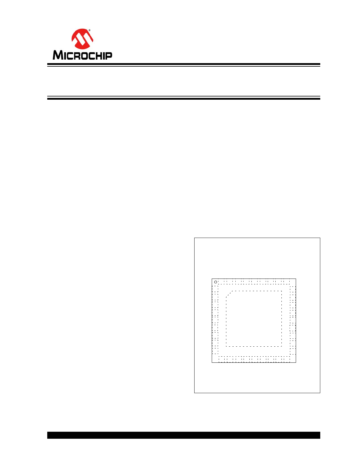
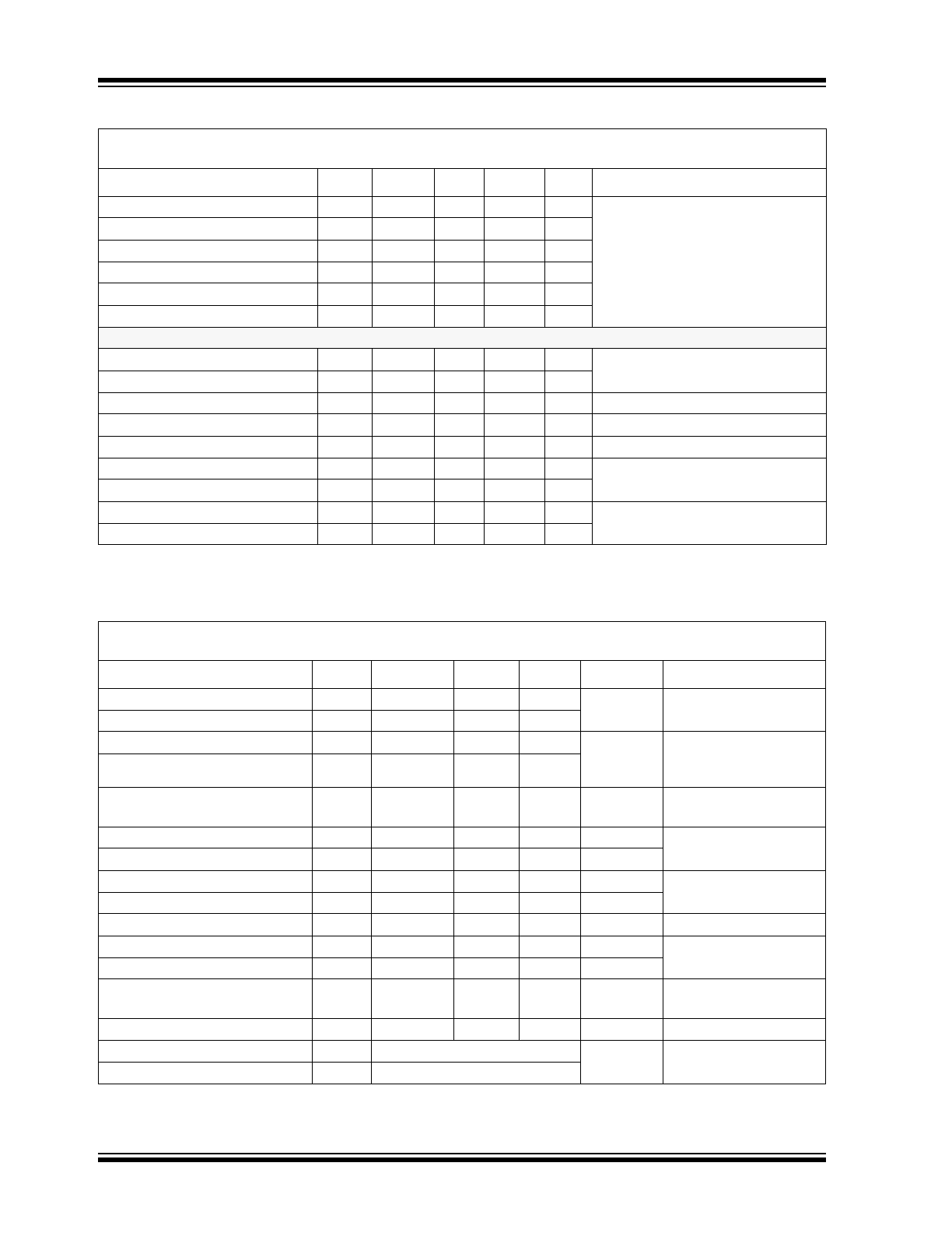
Package Type
2
CLKN
V
LL
EN
CBE1
SDO
CKB1
SPIB
CB
E0
CK
B0
GND
CLKP
EP
1
3
4
6
7
8
9
37
5
10
GND
TXR
W
V
GP
MD1730
6x6x0.9 mm 36-lead VQFN*
* Includes Exposed Thermal Pad (EP); see
Table 3-1
.
V
DD
SCK
CSN
SDI
11
15
12 13 14
18
17
16
26
27
25
24
22
21
20
19
23
36 35
31
34 33 32
28
29
30
V
GN
CN
F
V
CW
-
CPF
V
CW+
CW2
CW3
CW0
CW1
V
GN
CW4
CW5
CW6
CW7
CN
F
V
CW
-
CP
F
V
CW+
8-Channel Ultra-Low Phase Noise
Continuous Waveform Transmitter with Beamformer
MD1730
DS20005586B-page 2
2016 Microchip Technology Inc.
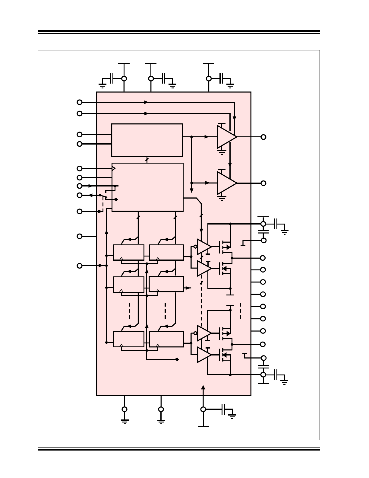
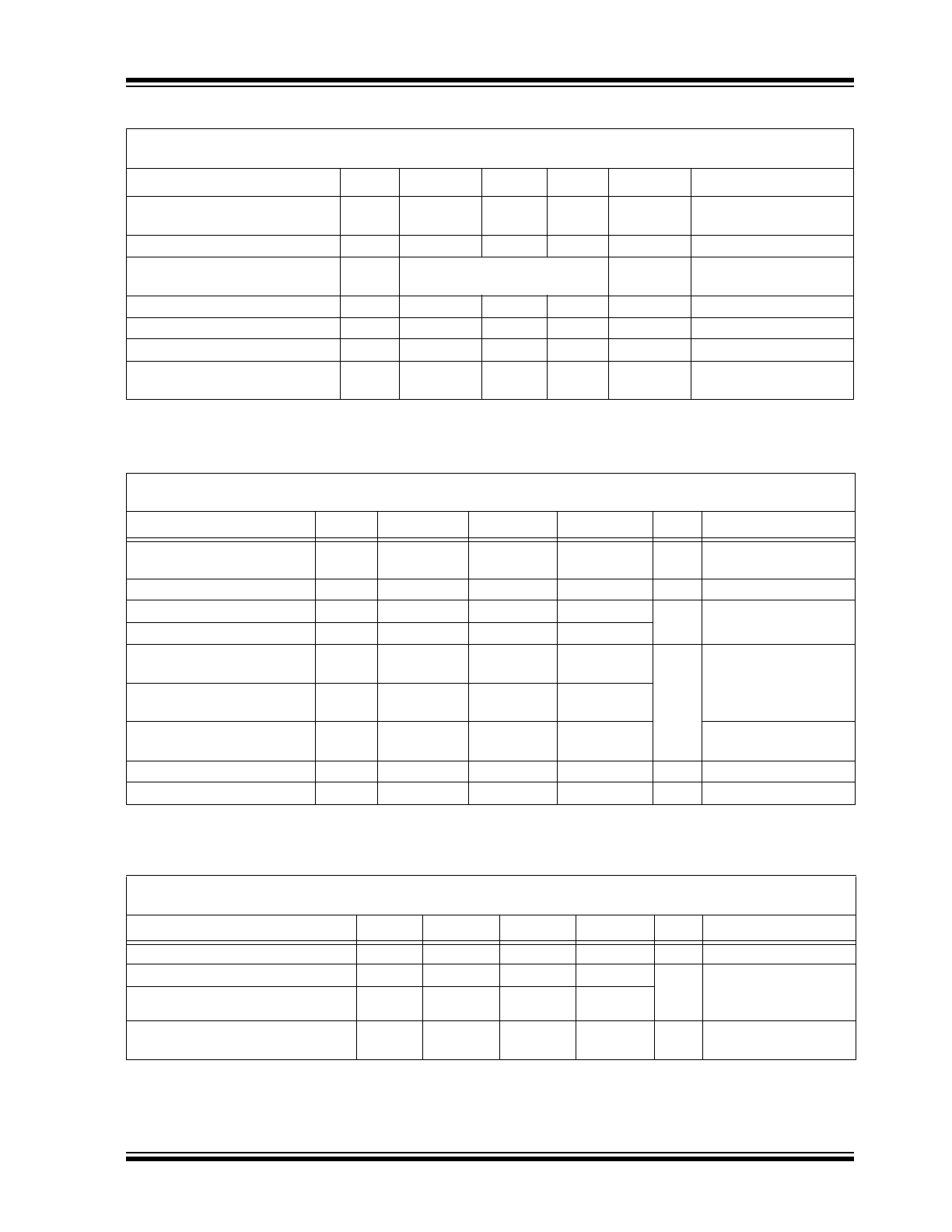
Block Diagram
0 to +
V C W +
C W 0
V P F
V NF
+10V
V
G P
E N
+2.5V
V
L L
T X R W
S P IB
S DI
C S N
S C K
C L K N
C L K P
LV DS / S S T L
C loc k Input
S P I
&
R egis ters
G ND
C W 1
MD1730
T hermal
P ad
-10V
S UB
V L L
C L K
C K B 0
C W 7
V P F
V NF
0 to -
V C W-
V C W +
V C W-
HIZ[7: 0]
C P F
V P F
V NF
C NF
S DO
Q
MS B
D
0
C K B 1
C B E 1
V L L
C B E 0
+5V
V
DD
V
G N
C L K
P HD7~0[7: 0] C W F D[7: 0]
P HD1[7: 0]
C W F D[7: 0]
E NA
E NA
Q
C L K
C L K
Q
P HD7[7: 0]
C W F D[7: 0]
E NA
E NA
Q
C L K
C L K
Q
8
64
C L K
S C K
V C W +
V C W-
1uF
1uF
2.2uF
2.2uF
1uF
1uF
1uF
1uF
P HD0[7: 0]
C W F D[7: 0]
E NA
E NA
Q
C L K
C L K
Q
C W 2
C W 3
C W 4
C W 5
C W 6
6V
6V
2016 Microchip Technology Inc.
DS20005586B-page 3
MD1730
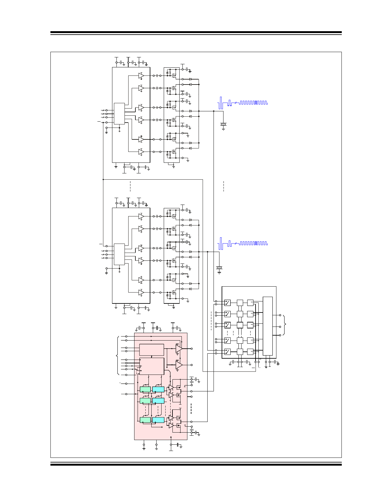
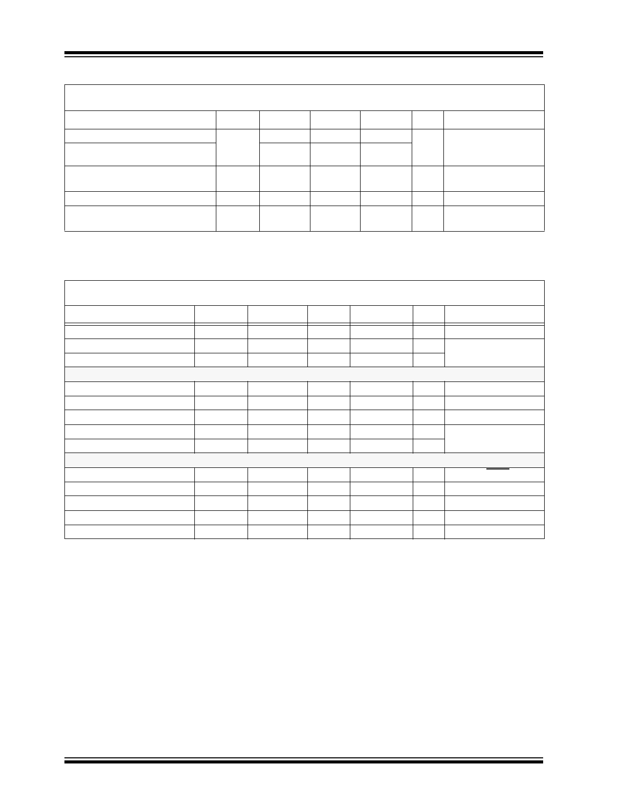
MD1730 CW Output via HV2201 Application Block Diagram
+10V
V GP
+2 to +6V
VCW+
CW0
VPF
VNF
EN
+2.5V
V LL
TXRW
SPIB
SDI
CSN
SCK
CLKN
CLKP
LVDS / SSLT
Clock Input
SPI
&
Registers
GND
CW1
MD1730
Thermal
Pad
-10V
SUB
VLL
CLK
CKB0
CW7
VPF
VNF
-2 to -6V
VCW-
VCW+
VCW-
HIZ[7:0]
CPF
VPF
VNF
CNF
SDO
Q
MSB
D
0
CKB1
CBE1
VLL
CBE0
+5V
V DD
V GN
CLK
PHD7~0[7:0]
CWFD[7:0]
PHD1[7:0]
CWFD[7:0]
ENA
ENA
Q
CLK
CLK
Q
PHD7[7:0]
CWFD[7:0]
ENA
ENA
Q
CLK
CLK
Q
PHD0[7:0]
CWFD[7:0]
ENA
ENA
Q
CLK
CLK
Q
8
64
CLK
SCK
VCW+
VCW-
XDCR
XDCR
D
LE
CL
SW0
D
LE
CL
SW1
D
LE
CL
SW2
D
LE
SW6
D
LE
CL
SW7
CLK
8-BIT
SHIFT
REGISTER
DIN
DOUT
LEVEL
SHIFTERS
OUTPUT
SWITCHES
VNN
VPP
CLR
LE
GND
VDD
LATCHES
CL
TX7
EN
SEL
POS
NEG
B/CW
LVL[3:2]
POS[3:2]
NEG[3:2]
V
DD2
High Speed
Gate Buffers
V
DD2
V
DD1
V
DD1
V
SS
V
DD1
High Speed
Gate Buffers
Control
Logic and
Level
Transla-
tion
GND
MD1715
1 of 2-ch
TC8020
6 of 12-FET
+10V
VDD2
+10V
VDD1
+10V
AVDD
+90V
SP1
+50V
SP2
-90V
SN1
-50V
DP1
DN1
DP2
DN2
SN2
SP3
SN3
DP3
DN3
GP1
GN1
GP2
GN2
GP3
GN3
OP1
ON1
OP2
ON2
OP3
ON3
-10V
VSS
-10V
AVSS
PAD
GND
PAD
VSUB
TX0
V
DD2
High Speed
Gate Buffers
V
DD2
V
DD1
V
DD1
V
SS
V
DD1
High Speed
Gate Buffers
Control
Logic and
Level
Transla-
tion
MD1715
1 of 2-ch
TC8020
6 of 12-FET
+10V
VDD2
+10V
VDD1
+10V
AVDD
+90V
SP1
+50V
SP2
-90V
SN1
-50V
DP1
DN1
DP2
DN2
SN2
SP3
SN3
DP3
DN3
GP1
GN1
GP2
GN2
GP3
GN3
OP1
ON1
OP2
ON2
OP3
ON3
-10V
VSS
-10V
AVSS
PAD
GND
PAD
VSUB
HV2201
8-ch HV Analog Switch
EN
SEL
POS
NEG
B/CW
LVL[1:0]
POS[1:0]
NEG[1:0]
GND
B/CW
LE
+3.3V
-100V +100V
CW/ B
CW_START
FPGA
FPGA

MD1730
DS20005586B-page 4
2016 Microchip Technology Inc.
NOTES:
2016 Microchip Technology Inc.
DS20005586B-page 5
MD1730
1.0
ELECTRICAL CHARACTERISTICS
Absolute Maximum Ratings †
Positive Logic Supply (V
LL
) ........................................................................................................................ -0.5V to +3.0V
Positive Supply Voltage (V
DD
).................................................................................................................... -0.5V to +6.0V
Positive Supply Voltage (V
GP
).................................................................................................................. -0.5V to +13.5V
Negative Supply Voltage (V
GN
)................................................................................................................ +0.5V to -13.5V
CW Output Positive Supply Voltage (V
CW+
) ............................................................................................... -0.5V to +12V
CW Output Negative Supply Voltage (V
CW-
)............................................................................................... +0.5V to -12V
All Digital Inputs (V
IN
)................................................................................................................................. -0.5V to +3.0V
CW Outputs (V
OUT
)...................................................................................................................................... -12V to +12V
Operating Ambient Temperature ................................................................................................................. 0°C to +85°C
Maximum Junction Temperature ................................................................................................................. 0°C to +85°C
Storage Temperature ............................................................................................................................................ +125°C
Thermal Resistance Junction to Ambient (Ɵ
JA
, JESD51-5)..................................................................................25°C/W
Thermal Resistance Junction to Bottom Cu Pad (Ɵ
JB
, JESD51-5) ....................................................................6.4°C/W
Thermal Resistance Junction to Package Top (Ɵ
JC
, JESD51-5).......................................................................13.5°C/W
ESD Rating All Pins ............................................................................................................................................. ±1.0 kV
† Notice:
Stresses above those listed under “Maximum Ratings” may cause permanent damage to the device. This is
a stress rating only and functional operation of the device at those or any other conditions above those indicated in the
operational sections of this specification is not intended. Exposure to maximum rating conditions for extended periods
may affect device reliability.
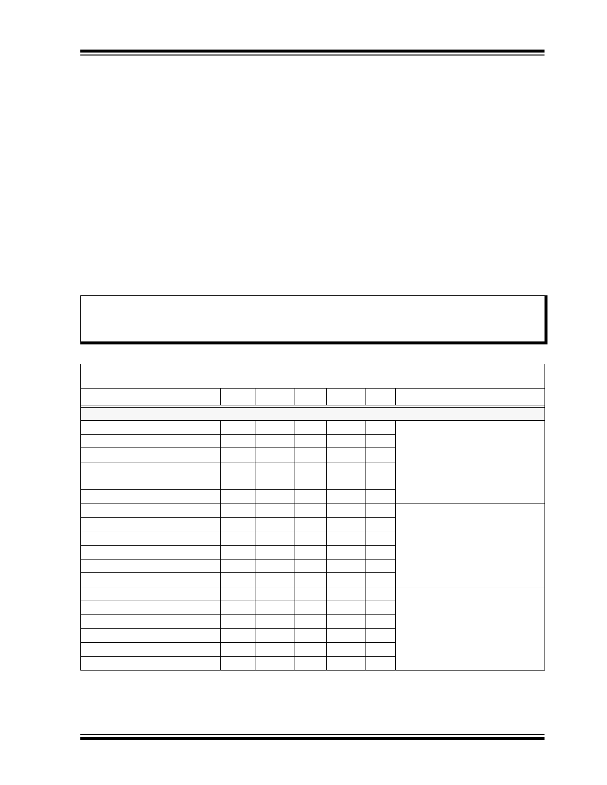
TABLE 1-1:
INPUT/OUTPUT PIN DC CHARACTERISTICS
Electrical Specifications:
Unless otherwise indicated, V
LL
= +2.5V, V
GP
= +10V, V
GN
= -10V, V
CW+
= +6.0V,
V
CW-
= -6.0V, V
DD
= +5V, T
A
= 25°C.
Parameters
Sym.
Min.
Typ.
Max.
Units
Conditions
Operating Supply
Logic Supply Voltage
V
LL
2.35
2.50
2.65
V
(V
GP
+|V
CW-
|) ≥ 10V
(V
GN
+|V
CW+
|) ≥ 10V
T
A
= 0 to +85°C,
Note 2
VDD Supply Voltage
V
DD
4.75
5.0
5.25
V
Positive Supply Voltage
V
GP
8.0
10
12
V
Negative Supply Voltage
V
GN
-12
-10
-8.0
V
CW Output Positive Supply
V
CW+
1.0
—
6.0
V
CW Output Negative Supply
V
CW-
-6.0
—
-1.0
V
V
LL
Quiescent Current
I
LLQ
—
0.02
0.1
mA
EN = 0, f
CLK
= f
SCK
= 0
All logic input no transit
V
DD
Quiescent Current
I
DDQ
—
0.15
0.2
mA
V
GP
Quiescent Current
I
GPQ
—
1.0
2.0
µA
V
GN
Quiescent Current
I
GNQ
—
33
45
µA
V
CW+
Quiescent Current
I
CW+Q
—
26
45
µA
V
CW-
Quiescent Current
I
CW-Q
—
6
10
µA
V
LL
Enabled Current
I
LLEN
—
6.0
9.0
mA
EN = 1, f
SCK
= 120 MHz
TXRW = 0, SDI = 0,
SDO no load.
V
DD
Enabled Current
I
DDEN
—
0.2
0.3
mA
V
GP
Enabled Current
I
GPEN
—
2.0
3.0
mA
V
GN
Enabled Current
I
GNEN
—
2.0
3.0
mA
V
CW+
Enabled Current
I
CW+EN
—
2.0
3.0
mA
V
CW-
Enabled Current
I
CW-EN
—
2.0
3.0
mA
Note 1:
Characterized only; not 100% tested in production.
2:
Design Guidance Only (DGO).
MD1730
DS20005586B-page 6
2016 Microchip Technology Inc.
V
LL
Current at CW 5MHz
I
LL5
—
2.5
3.0
mA
EN = 1, f
CLK
= 80 MHz,
TXRW = 1, CW 5 MHz,
no load 8-channel
V
DD
Current at CW 5MHz
I
DD5
—
1.0
2.0
mA
V
GP
Current at CW 5MHz
I
GP5
—
6.0
10
mA
V
GN
Current at CW 5MHz
I
GN5
—
12
18
mA
V
CW+
Current at CW 5MHz
I
CW+5
—
26
35
mA
V
CW-
Current at CW 5MHz
I
CW-5
—
21
30
mA
SPI & Logic
Input Logic High Voltage
V
IH
0.8 V
LL
—
V
LL
V
2.5V LVCMOS
Input Logic Low Voltage
V
IL
0
—
0.2 V
LL
V
Input Logic High Current
I
IH
—
—
1.0
µA
Input Logic Low Current
I
IL
—
—
µA
SPI and Logic Input Capacitance
C
IN
—
4.5
—
pF
Note 1
Output Logic High Current
I
OH
—
—
mA
2.5V LVCMOS
Output Logic Low Current
I
OL
—
—
mA
SDO Output Logic High Voltage
V
OH
—
—
V
with 5 pF load
SDO Output Logic Low Voltage
V
OL
—
—
0.35
V
TABLE 1-2:
SPI AND LOGIC AC ELECTRICAL SPECIFICATIONS
Electrical Specifications:
Unless otherwise indicated, V
LL
= +2.5V, V
GP
= +10V, V
GN
= -10V, V
CW+
= +6.0V,
V
CW-
= -6.0V, V
DD
= +5V, T
A
= 25°C.
Parameters
Sym.
Min.
Typ.
Max.
Units
Conditions
Output Rise Time
t
r
—
0.65
—
ns
1.5 pF load,
Note 1
Output Fall Time
t
f
—
0.65
—
Output Rise Propagation Delay
t
dr
—
2.8
—
ns
CLK rise 50% to output
50%, after latency.
Note 1
Output Fall Propagation Delay
t
df
—
3.0
—
Delay Time Matching
t
dm
—
±0.5
±1.0
ns
Channel to channel,
Note 1
, f
CLK
= 80 MHz
SDI Valid to SCK, Setup Time
t
1
0.6
1.0
—
ns
Note 1
SCK To SDI Data Hold Time
t
2
2.0
—
—
ns
SCK High Time % of 1/f
CLK
t
3
45
—
55
%
Note 2
SCK Low Time % of 1/f
CLK
t
4
45
—
55
%
CSN Hi-Time
t
5
2-cycle
—
—
SCK
Note 2
SCK Rise to CSN Rise
t
6
—
2.0
—
ns
Note 1
CSN Low to SCK Rise
t
7
—
0.8
—
ns
SDO Valid from SCK Rise
t
8
—
3.1
4.0
ns
SPIB = 0, 1.5 pF Load,
Note 1
CSN Rise to SCK Rise
t
9
—
2.0
—
ns
Note 1
CSN Rise to TXRW or SPIB Rise
t
10
9-cycle
SCK
Note 2
TXRW or SPIB Fall to CSN Fall
t
11
1-cycle
Note 1:
Characterized only; not 100% tested in production.
2:
Design Guidance Only (DGO).
TABLE 1-1:
INPUT/OUTPUT PIN DC CHARACTERISTICS (CONTINUED)
Electrical Specifications:
Unless otherwise indicated, V
LL
= +2.5V, V
GP
= +10V, V
GN
= -10V, V
CW+
= +6.0V,
V
CW-
= -6.0V, V
DD
= +5V, T
A
= 25°C.
Parameters
Sym.
Min.
Typ.
Max.
Units
Conditions
Note 1:
Characterized only; not 100% tested in production.
2:
Design Guidance Only (DGO).
2016 Microchip Technology Inc.
DS20005586B-page 7
MD1730
SDO to SDI Valid Delay
t
12
—
2.3
3.0
ns
SPIB = 1, 1.5 pF Load,
Note 1
TXRW Rise to CLKP Rise
t
13
—
2.5
—
ns
Note 1
Latency to CW Wave Rise
t
14
2-cycle
CLK
After TXRW = 1,
PHD=0,
Note 2
Latency CSN Rise to TXRW Fall
t
15
2-cycle
—
—
CLK
Note 2
SCK Clock Frequency
f
SCK
—
—
200
MHz
Note 1
EN Off Time
t
EN-Off
—
20
30
ns
Note 2
EN On Time
t
EN-On
—
150
300
µs
2.0 µF on CPF/CNF,
Note 2
TABLE 1-3:
CLOCK BUFFER OUTPUTS AC/DC CHARACTERISTICS
Electrical Specifications:
Unless otherwise indicated, V
LL
= +2.5V, V
GP
= +10V, V
GN
= -10V, V
CW+
= +6.0V,
V
CW-
= -6.0V, V
DD
= +5V, T
A
= 25°C.
Parameters
Sym.
Min.
Typ.
Max.
Units
Conditions
Clock Output Frequency
Range
f
CKB
40
160
250
MHz
Note 1
Clock Output Duty Cycle
D%
45
—
55
%
Note 2
CKB0,1 Rise Time
t
rb
—
0.6
1.0
ns
f
CLK
= 80 Mhz, 1.5 pF
load,
Note 1
CKB0,1 Fall Time
t
fb
—
0.5
1.0
Output Rise Propagation
Delay
t
drb
—
2.0
3.0
ns
CLK rise to CKB, 50%,
Note 1
Output Fall Propagation
Delay
t
dfb
—
2.0
3.0
CBE Enable Time
t
cbe
—
2.1
3.0
CBE to CLK rise, 50%,
Note 1
CKB0,1 Output logic high
V
OHCKB
—
V
LL
—
V
Note 2
CKB0,1 Output Logic low
V
OLCKB
—
GND
—
V
Note 2
Note 1:
Characterized only; not 100% tested in production.
2:
Design Guidance Only (DGO).
TABLE 1-4:
CW OUTPUTS DC/AC ELECTRICAL CHARACTERISTICS
Electrical Specifications:
Unless otherwise indicated, V
LL
= +2.5V, V
GP
= +10V, V
GN
= -10V, V
CW+
= +6.0V,
V
CW-
= -6.0V, V
DD
= +5V, T
A
= 25°C.
Parameters
Sym.
Min.
Typ.
Max.
Units
Conditions
CW Output Peak to Peak Voltage
V
CWOUT
-6.0
-
+6.0
V
CW Output Rise Propagation Delay
t
drCW
—
4.0
6.0
ns
TxCLK 50% to CWx
10%, after latency,
Note 1
CW Output Fall Propagation Delay
t
dfCW
—
4.0
6.0
CW Output Maximum Current
I
CW±
±250
±300
—
mA
V
CW±
= ±5.0V, 0.1Ω
load,
Note 1
Note 1:
Characterized only; not 100% tested in production.
2:
Design Guidance Only (DGO).
TABLE 1-2:
SPI AND LOGIC AC ELECTRICAL SPECIFICATIONS (CONTINUED)
Electrical Specifications:
Unless otherwise indicated, V
LL
= +2.5V, V
GP
= +10V, V
GN
= -10V, V
CW+
= +6.0V,
V
CW-
= -6.0V, V
DD
= +5V, T
A
= 25°C.
Parameters
Sym.
Min.
Typ.
Max.
Units
Conditions
Note 1:
Characterized only; not 100% tested in production.
2:
Design Guidance Only (DGO).
MD1730
DS20005586B-page 8
2016 Microchip Technology Inc.
Static Output Resistance PFET
R
ONCW
—
7.5
12
Ω
RON at V
CW±
= ±5.0V,
I
CW±
= ±100 mA load,
Note 1
Static Output Resistance NFET
—
6.5
11
Change in R
DS(ON)
with
Temperature
∆R
ONCW
—
—
1.0
%/C
V
CW±
= ±5.0V,
Note 2
CW Phase Resolution
RE
Phase
—
1
—
CLK
Note 2
CW Phase Noise
N
Phase
—
-160
—
dBC/
Hz
CW 5 MHz,
1 kHz Offset,
Note 1
Note 1:
Characterized only; not 100% tested in production.
2:
Design Guidance Only (DGO).
TABLE 1-4:
CW OUTPUTS DC/AC ELECTRICAL CHARACTERISTICS (CONTINUED)
Electrical Specifications:
Unless otherwise indicated, V
LL
= +2.5V, V
GP
= +10V, V
GN
= -10V, V
CW+
= +6.0V,
V
CW-
= -6.0V, V
DD
= +5V, T
A
= 25°C.
Parameters
Sym.
Min.
Typ.
Max.
Units
Conditions
TABLE 1-5:
LVDS / SSTL CLOCK INPUTS AC / DC CHARACTERISTICS
Electrical Specifications:
Unless otherwise indicated, V
LL
= +2.5V, V
GP
= +10V, V
GN
= -10V, V
CW+
= +6.0V,
V
CW-
= -6.0V, V
DD
= +5V, T
A
= 25°C.
Parameters
Sym.
Min.
Typ.
Max.
Units
Conditions
CLKP/CLKN Clock Frequency
f
CLK
40
160
250
MHz
Note 1
Clock Input Slew Rate
t
CSR
1.0
—
—
V/ns
Note 2
Control/Data Input Slew Rate
t
DSR
1.0
—
—
V/ns
Single Ended Clock Input
SSTL Reference Voltage
V
REFS
1.13
1.25
1.38
V
Note 1
DC Input Logic High
V
IH(DC)
V
REFS
+0.15
—
V
LL
+0.3
V
Note 1
DC Input Logic Low
V
IL(DC)
-0.3
—
V
REFS
-0.15
V
Note 1
AC Input Logic High
V
IH(AC)
V
REFS
+0.31
—
—
V
V
REF
= 0.5V
LL
, Slew
rate 1.0 V/ns,
Note 1
AC Input Logic Low
V
IL(AC)
-
—
V
REFS
-0.31
V
Differential Clock Input
AC Differential Cross Point
V
X(AC)
0.5V
LL
-0.2
—
0.5V
LL
+0.2
V
CLK and CLK,
Note 1
DC Input Max Swing Voltage
V
SWING(DC)
0.3
—
V
LL
+0.6
V
Note 1
AC Differential Input Voltage
V
SWING(AC)
0.62
—
V
LL
+0.6
V
Note 1
DC Input Signal Voltage
V
IN(DC)
-0.3
—
V
LL
+0.3
V
Note 1
CLKP/CLKN Slew Rate
SLEW
1.0
—
—
V/ns
Note 2
Note 1:
Characterized only; not 100% tested in production.
2:
Design Guidance Only (DGO).

2016 Microchip Technology Inc.
DS20005586B-page 9
MD1730
NOTES:
MD1730
DS20005586B-page 10
2016 Microchip Technology Inc.
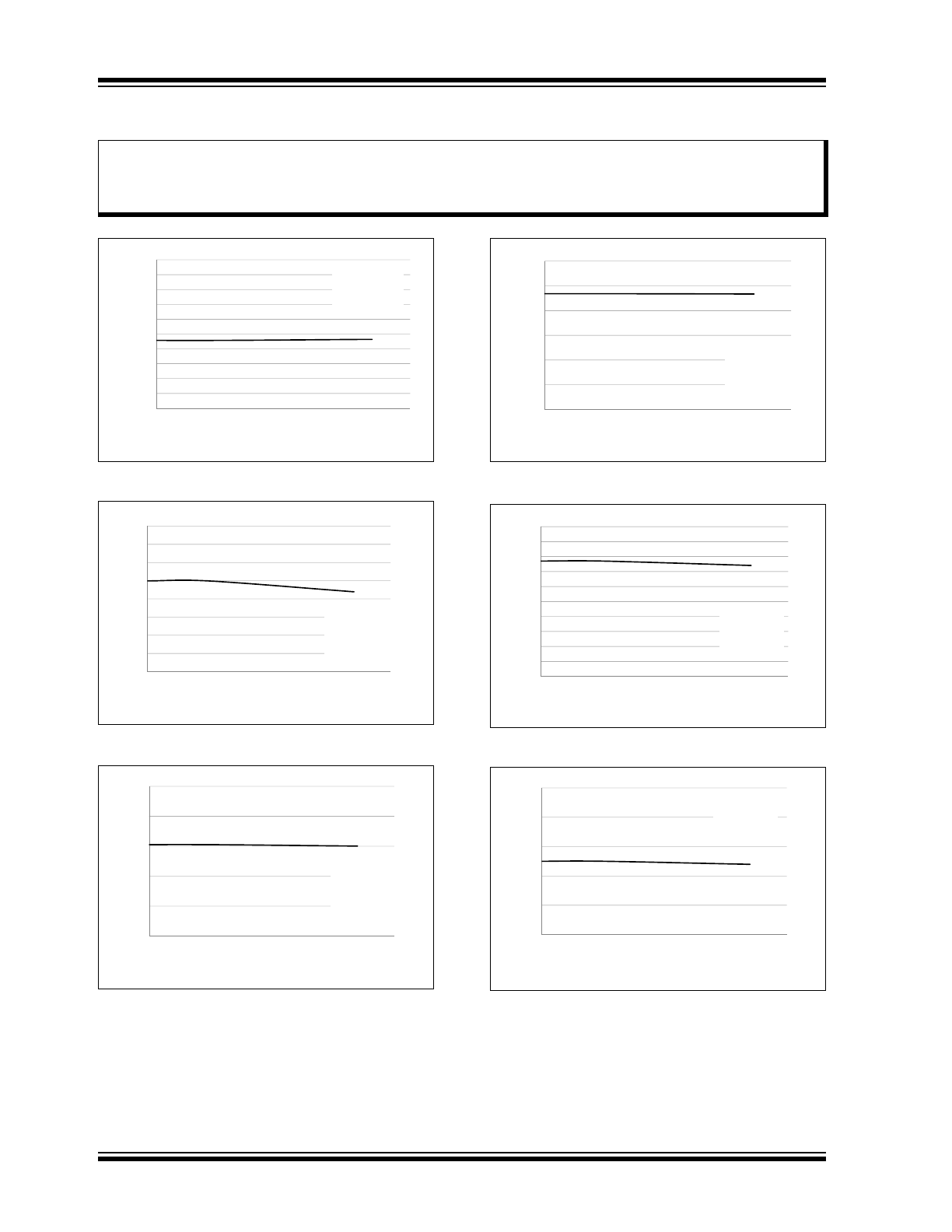
2.0
TYPICAL PERFORMANCE CURVES
FIGURE 2-1:
I
DD
vs. Temperature.
FIGURE 2-2:
I
VGP
vs. Temperature.
FIGURE 2-3:
I
VCW+
vs. Temperature.
FIGURE 2-4:
I
VLL
vs. Temperature.
FIGURE 2-5:
I
VGN
vs. Temperature.
FIGURE 2-6:
I
VCW-
vs. Temperature.
Note:
The graphs and tables provided following this note are a statistical summary based on a limited number of
samples and are provided for informational purposes only. The performance characteristics listed herein
are not tested or guaranteed. In some graphs or tables, the data presented may be outside the specified
operating range (e.g., outside specified power supply range) and therefore outside the warranted range.
0
0.1
0.2
0.3
0.4
0.5
0.6
0.7
0.8
0.9
1
0
10
20
30
40
50
60
70
80
90
100
Current (m
A)
Temperature (°C)
V
DD
= 5.0V,
f
CLK
= 80 MHz,
f
CW
= 5 MHz,
8-ch, no-load
0
1
2
3
4
5
6
7
8
0
10
20
30
40
50
60
70
80
90 100
Current (mA)
Temperature (°C)
V
GP
= 10V,
f
CLK
= 80 MHz,
f
CW
= 5 MHz,
8-ch, no-load
0
5
10
15
20
25
0
10
20
30
40
50
60
70
80
90 100
Current (mA)
Temperature (°C)
V
CW+
= 5V,
f
CLK
= 80 MHz,
f
CW
= 5 MHz,
8-ch, no-load
0
0.5
1
1.5
2
2.5
3
0
10
20
30
40
50
60
70
80
90
100
Current
(mA)
Temperature (°C)
V
DD
= 2.5V,
f
CLK
= 80 MHz,
f
CW
= 5 MHz,
8-ch, no-load
0
1
2
3
4
5
6
7
8
9
10
0
10
20
30
40
50
60
70
80
90
100
Current (mA)
Temperature (°C)
V
GN
= -10V,
f
CLK
= 80 MHz,
f
CW
= 5 MHz,
8-ch, no-load
0
5
10
15
20
25
0
10
20
30
40
50
60
70
80
90 100
Curre
nt (mA)
Temperature (°C)
V
CW-
= -5V,
f
CLK
= 80 MHz,
f
CW
= 5 MHz,
8-ch, no-load