
2016 Microchip Technology Inc.
DS20005638A-page 1
MIC5891
Features
• High-Voltage, High-Current Outputs
• Output Transient Protection Diodes
• CMOS-, PMOS-, NMOS-, and TTL-Compatible
Inputs
• 5 MHz Typical Data Input Rate
• Low-Power CMOS Latches
Applications
• Alphanumeric and Bar Graph Displays
• LED and Incandescent Displays
• Relay and Solenoid Drivers
• Other High-Power Loads
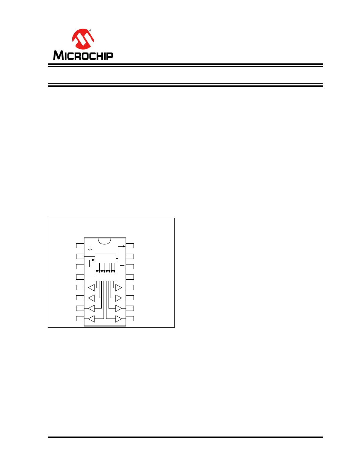
Package Type
General Description
The MIC5891 latched driver is a high-voltage,
high-current integrated circuit comprised of eight
CMOS data latches, CMOS control circuitry for the
common STROBE and OUTPUT ENABLE, and bipolar
Darlington transistor drivers for each latch.
Bipolar/MOS construction provides extremely low
power latches with maximum interface flexibility.
The MIC5891 will typically operate at 5 MHz with a 5V
logic supply.
The CMOS inputs are compatible with standard
CMOS, PMOS, and NMOS logic levels. TTL circuits
may be used with appropriate pull-up resistors to
ensure a proper logic-high input.
A CMOS serial data output allows additional drivers to
be cascaded when more than 8 bits are required.
The MIC5891 has open-emitter outputs with
suppression diodes for protection against inductive
load transients. The output transistors are capable of
sourcing 500 mA and will sustain at least 35V in the
on-state.
Simultaneous operation of all drivers at maximum rated
current requires a reduction in duty cycle due to
package power limitations. Outputs may be paralleled
for higher load current capability.
The MIC5891 is available in a 16-pin plastic DIP
package (N) and 16-pin wide SOIC package (WM).
STROBE 4
SERIAL
DATA IN 3
CLOCK 2
GROUND 1
OUT
3
7
OUT
2
6
OUT
1
5
OUT
4
8
LOAD SUPPLY
13
OUTPUT
ENABLE
14
LOGIC SUPPLY
15
SERIAL
DATA OUT
16
OUT
6
10
OUT
7
11
OUT
8
12
OUT
5
9
V
BB
V
DD
OE
SHIFT
REGISTER
LATCHES
MIC5891
16-P
IN
PDIP
OR
SOICW
8-Bit Serial-Input Latched Source Driver
MIC5891
DS20005638A-page 2
2016 Microchip Technology Inc.
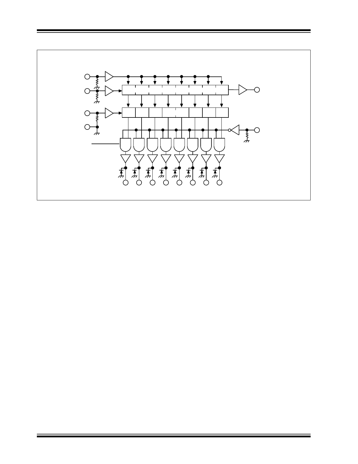
Functional Diagram
MIC5891
16-P
IN
PDIP
OR
SOICW
OUT
1
OUT
2
OUT
3
OUT
4
OUT
5
OUT
6
OUT
7
OUT
8
SERIAL
DATA OUT
OUTPUT
ENABLE
CLOCK
SERIAL
DATA IN
STROBE
GROUND
8-BIT SERIAL PARALLEL SHIFT REGISTER
LATCHES
MOS
BIPOLAR
2016 Microchip Technology Inc.
DS20005638A-page 3
MIC5891
1.0
ELECTRICAL CHARACTERISTICS
Absolute Maximum Ratings † (
Note 1
,
Note 2
,
Note 3
)
Output Voltage (V
OUT
) ..............................................................................................................................................+50V
Logic Supply Voltage Range (V
DD
) ............................................................................................................ +4.5V to +15V
Load Supply Voltage Range (V
BB
) ............................................................................................................. +5.0V to +50V
Input Voltage Range (V
IN
).............................................................................................................. –0.3V to (V
DD
+ 0.3V)
Continuous Collector Current (I
C
) .........................................................................................................................500 mA
Package Power Dissipation ...................................................................................................................... See
Figure 2-1
†
Notice: Stresses above those listed under “Absolute Maximum Ratings” may cause permanent damage to the device.
This is a stress rating only and functional operation of the device at those or any other conditions above those indicated
in the operational sections of this specification is not intended. Exposure to maximum rating conditions for extended
periods may affect device reliability.
Note 1:
T
A
= +25°C.
2:
Derate at the rate of 20 mW/°C above T
A
= +25°C.
3:
Microchip CMOS devices have input-static protection, but are susceptible to damage when exposed to
extremely high static electrical charges.
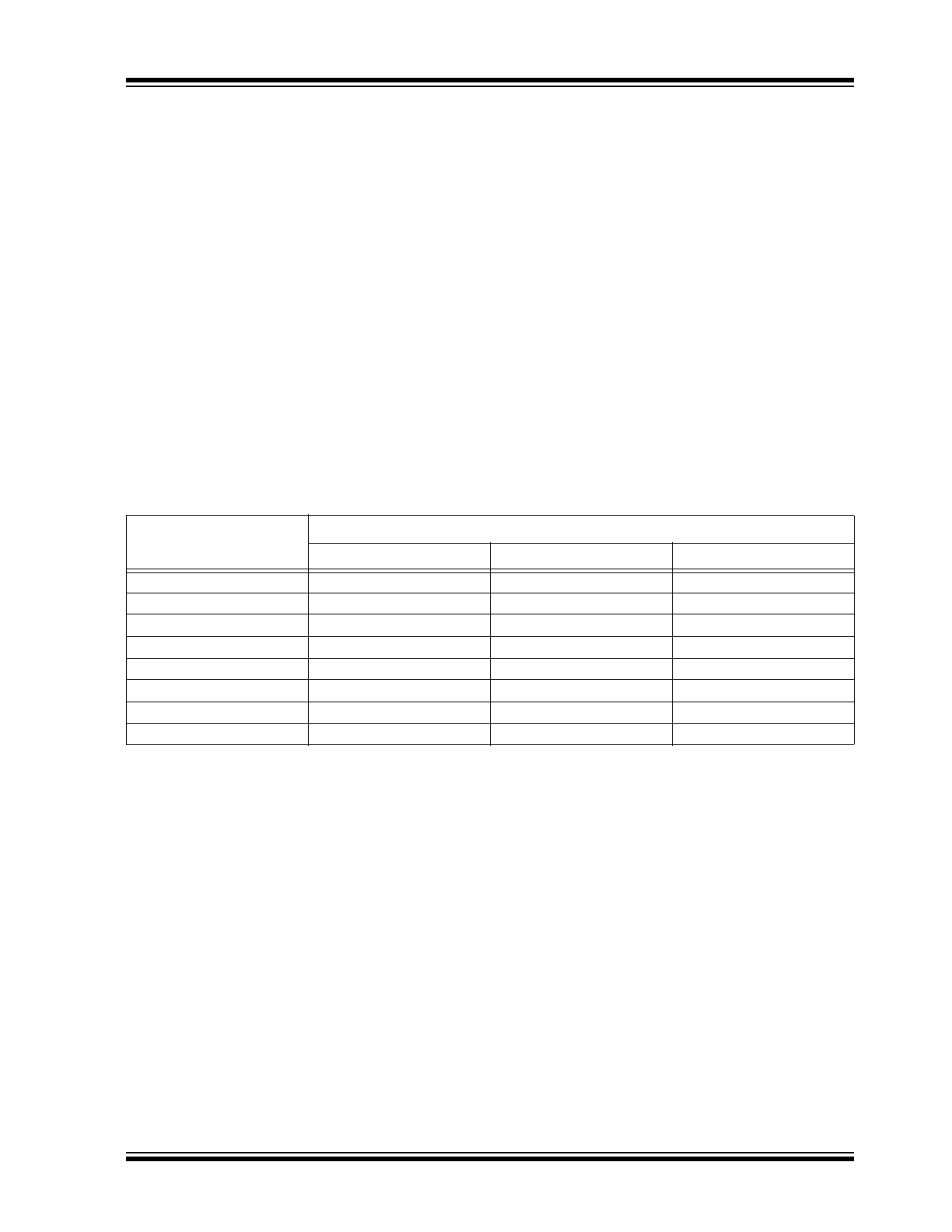
TABLE 1-1:
ALLOWABLE DUTY CYCLES
Number of Outputs ON at
I
OUT
= –200 mA
Maximum Allowable Duty Cycles at a T
A
of:
+50°C
+60°C
+70°C
8
53%
47%
41%
7
60%
54%
48%
6
70%
64%
56%
5
83%
75%
67%
4
100%
94%
84%
3
100%
100%
100%
2
100%
100%
100%
1
100%
100%
100%
MIC5891
DS20005638A-page 4
2016 Microchip Technology Inc.
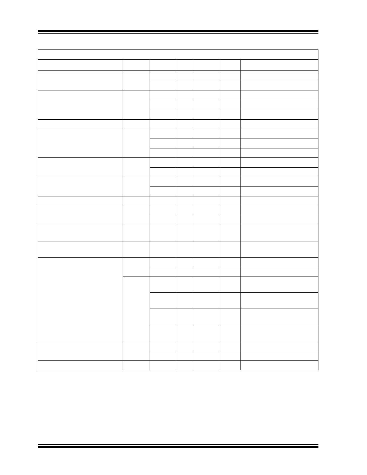
TABLE 1-2:
ELECTRICAL CHARACTERISTICS
Electrical Characteristics:
V
BB
= 50V, V
DD
= 5V to 12V; T
A
= 25°C, unless noted. (
Note 1
)
.
Parameters
Sym.
Min.
Typ.
Max.
Units
Conditions
Output Leakage Current
I
CEX
—
—
–50
µA
T
A
= +25°C
—
—
–100
µA
T
A
= +85°C
Output Saturation Voltage
V
CE(SAT)
—
—
2.3
V
I
OUT
= –100 mA, T
A
= +85°C
—
—
2.4
V
I
OUT
= –225 mA, T
A
= +85°C
—
—
2.5
V
I
OUT
= –350 mA, T
A
= +85°C
Output Sustaining Voltage
V
CE(SUS)
35
—
—
V
I
OUT
= –350 mA, L = 2 mH
Input Voltage
V
IN(1)
V
IN(0)
3.5
—
V
DD
+0.3
V
V
DD
= 5.0V
10.5
—
V
DD
+0.3
V
V
DD
= 12V
V
SS
–0.3
—
0.8
V
V
DD
= 5.0V to 12V
Input Current
I
IN(1)
—
—
120
µA
V
DD
= V
IN
= 5.0V
—
—
240
µA
V
DD
= 12V
Input Impedance
Z
IN
100
—
—
kΩ
V
DD
= 5.0V
50
—
—
kΩ
V
DD
= 12V
Maximum Clock Frequency
f
c
3.3
—
—
MHz
—
Serial Data Output Resistance
R
OUT
—
—
20
kΩ
V
DD
= 5.0V
—
—
6.0
kΩ
V
DD
= 12V
Turn-On Delay
t
PLH
—
—
2.0
µs
Output Enable to Output,
I
OUT
= –350 mA
Turn-Off Delay
t
PHL
—
—
10
µs
Output Enable to Output,
I
OUT
= –350 mA
Supply Current
I
BB
—
—
10
mA
All outputs on, all outputs open
—
—
200
µA
All outputs off
I
DD
—
—
100
µA
V
DD
= 5V, all outputs off,
inputs = 0V
—
—
200
µA
V
DD
= 12V, all outputs off,
inputs = 0V
—
—
1.0
mA
V
DD
= 5V, one output on,
inputs = 0V
—
—
3.0
mA
V
DD
= 12V, one output on,
inputs = 0V
Diode Leakage Current
I
H
—
—
50
µA
T
A
= +25°C; Max. V
BB
—
—
100
µA
T
A
= +85°C; Max. V
BB
Diode Forward Voltage
V
F
—
—
2.0
V
I
F
= 350 mA; V
BB
open
Note 1:
Specification for packaged product only.
2:
Positive (negative) current is defined as going into (coming out of) the specified device pin.
3:
Operation of these devices with standard TTL may require the use of appropriate pull-up resistors.
2016 Microchip Technology Inc.
DS20005638A-page 5
MIC5891
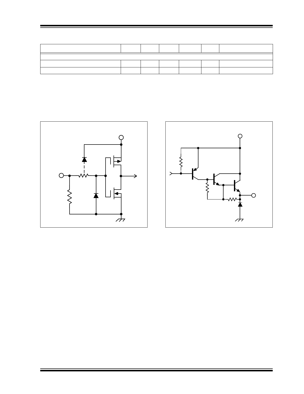
Typical Circuits
FIGURE 1-1:
Typical Input Circuit
FIGURE 1-2:
Typical Output Circuit.
TEMPERATURE SPECIFICATIONS
Parameters
Sym.
Min.
Typ.
Max.
Units
Conditions
Temperature Ranges
Operating Temperature Range
T
A
–40
—
+85
°C
Note 1
Storage Temperature Range
T
S
–65
—
+150
°C
—
Note 1:
The maximum allowable power dissipation is a function of ambient temperature, the maximum allowable
junction temperature and the thermal resistance from junction to air (i.e., T
A
, T
J
,
JA
). Exceeding the
maximum allowable power dissipation will cause the device operating junction temperature to exceed the
maximum +125°C rating. Sustained junction temperatures above +125°C can impact the device reliability.
IN
V
DD
V
BB
V
OUT
MIC5891
DS20005638A-page 6
2016 Microchip Technology Inc.
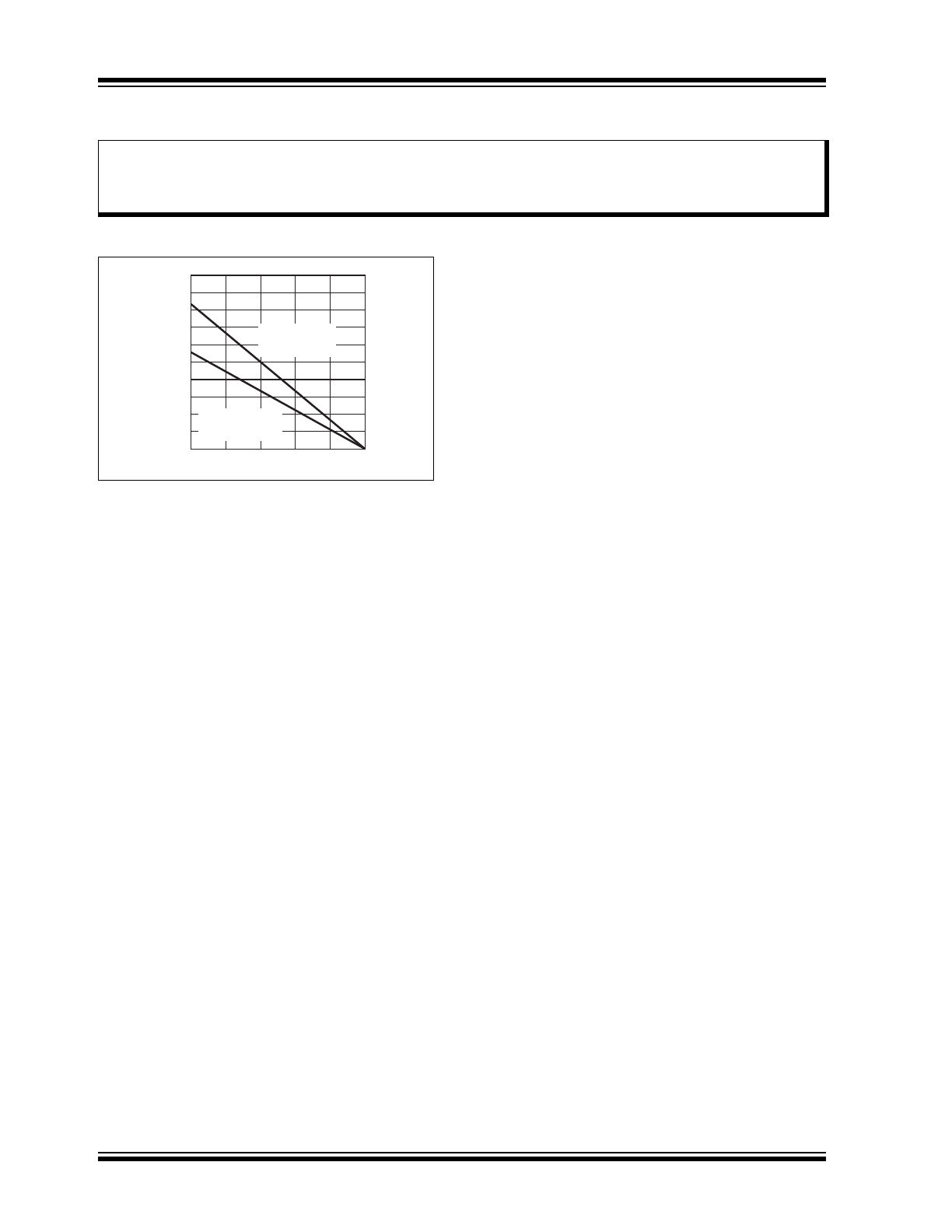
2.0
TYPICAL PERFORMANCE CURVES
FIGURE 2-1:
Allowable Package Power
Dissipation vs. Temperature.
Note:
The graphs and tables provided following this note are a statistical summary based on a limited number of
samples and are provided for informational purposes only. The performance characteristics listed herein
are not tested or guaranteed. In some graphs or tables, the data presented may be outside the specified
operating range (e.g., outside specified power supply range) and therefore outside the warranted range.
0
0.5
1
1.5
2
2.5
25
50
75
100
125
150
PACKAGE POWER DISSIPATION (W)
AMBIENT TEMPERATURE (°C)
PDIP
JA
= 60°C/W
CerDIP
JA
= 90°C/W
ș
ș
2016 Microchip Technology Inc.
DS20005638A-page 7
MIC5891
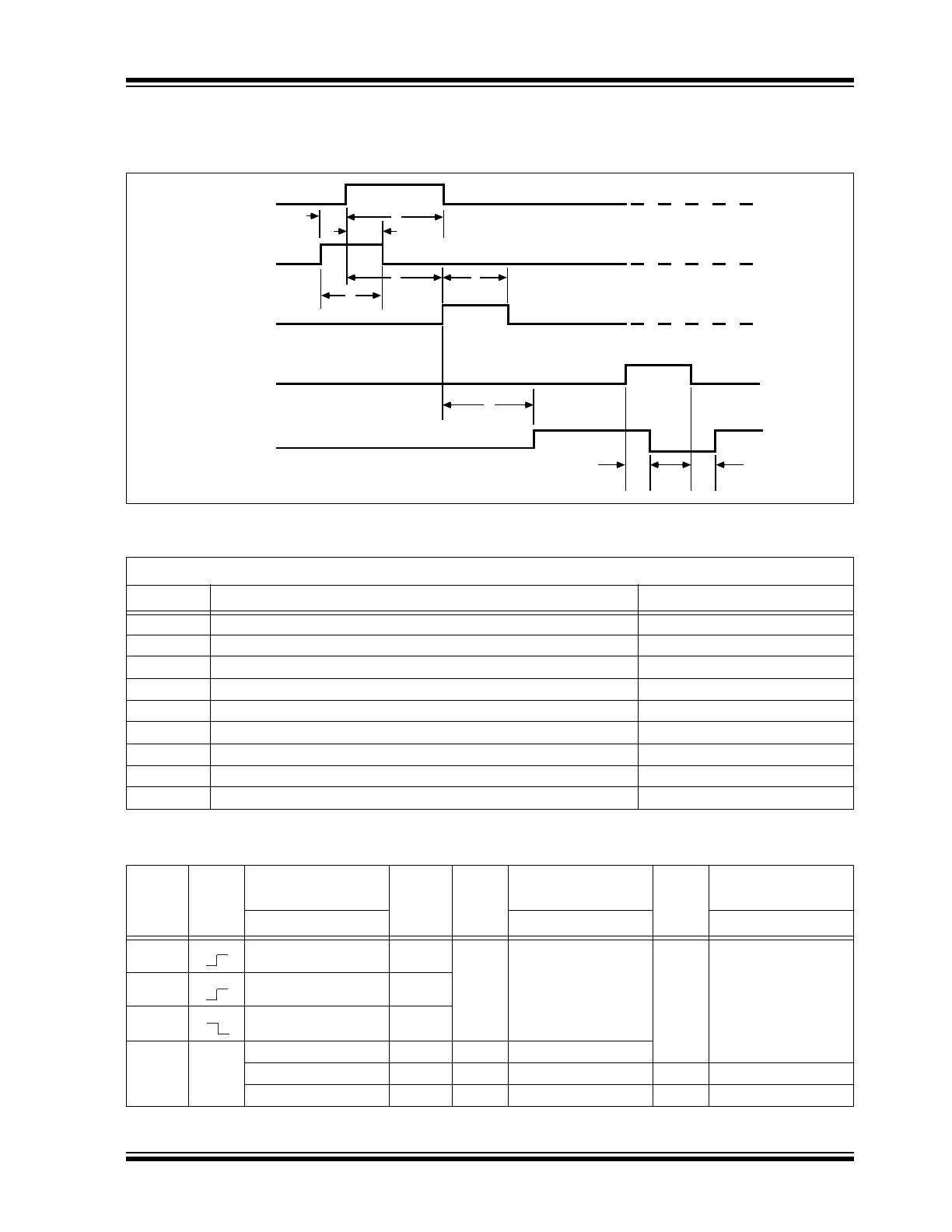
3.0
TIMING CONDITIONS
The descriptions of the timing conditions are listed below
Figure 3-1
.
FIGURE 3-1:
Timing Conditions.
L = Low Logic Level, H = High Logic Level, X = Irrelevant, P = Present State, R = Previous State.
TABLE 3-1:
TIMING CONDITIONS PARAMETERS
V
DD
= 5.0V, Logic levels are V
DD
and ground.
Reference
Parameter
Value
A
Minimum data active time before clock pulse (data set-up time)
75 ns
B
Minimum data active time after clock pulse (data hold time)
75 ns
C
Minimum data pulse width
150 ns
D
Minimum clock pulse width
150 ns
E
Minimum time between clock activation and strobe
300 ns
F
Minimum strobe pulse width
100 ns
G
Typical time between strobe activation and output transition
1.0 µs
H
Turn-off delay
See
Electrical Characteristics
I
Turn-on delay
See
Electrical Characteristics
CLOCK
DATA IN
STROBE
OUTPUT
ENABLE
OUTN
B
D
F
E
C
G
A
H
I
TABLE 3-2:
TRUTH TABLE
Serial
Data
Input
Clock
Input
Shift Register
Contents
Serial
Data
Output
Strobe
Input
Latch Contents
Output
Enable
Output Content
I
1
I
2
I
3
... I
N-1
I
N
I
1
I
2
I
3
... I
N-1
I
N
I
1
I
2
I
3
... I
N-1
I
N
H
H R
1
R
2
... R
N-2
R
N-1
R
N-1
—
—
—
—
L
L R
1
R
2
... R
N-2
R
N-1
R
N-1
X
R
1
R
2
R
3
... R
N-1
R
N
R
N
—
—
X X X ... X X
X
L
R
1
R
2
R
3
... R
N-1
R
N
P
1
P
2
P
3
... P
N-1
P
N
P
N
H
P
1
P
2
P
3
... P
N-1
P
N
L
P
1
P
2
P
3
... P
N-1
P
N
—
—
—
X X X ... X X
H
L L L ... L L

MIC5891
DS20005638A-page 8
2016 Microchip Technology Inc.
4.0
APPLICATION INFORMATION
Serial data present at the input is transferred into the
shift register on the rising edge of the CLOCK input
pulse. Additional CLOCK pulses shift data information
towards the SERIAL DATA OUTPUT. The serial data
must appear at the input prior to the rising edge of the
CLOCK input waveform.
The 8 bits present in the shift register are transferred to
the respective latches when the STROBE is high
(serial-to-parallel conversion). The latches will continue
to accept new data as long as the STROBE is held
high. Most applications where the latching feature is
not used (STROBE tied high) require the OUTPUT
ENABLE input to be high during serial data entry.
Outputs are active (controlled by the latch state) when
the OUTPUT ENABLE is low. All outputs are low
(disabled) when the OUTPUT ENABLE is high.
OUTPUT ENABLE does not affect the data in the shift
register or latch.
2016 Microchip Technology Inc.
DS20005638A-page 9
MIC5891
5.0
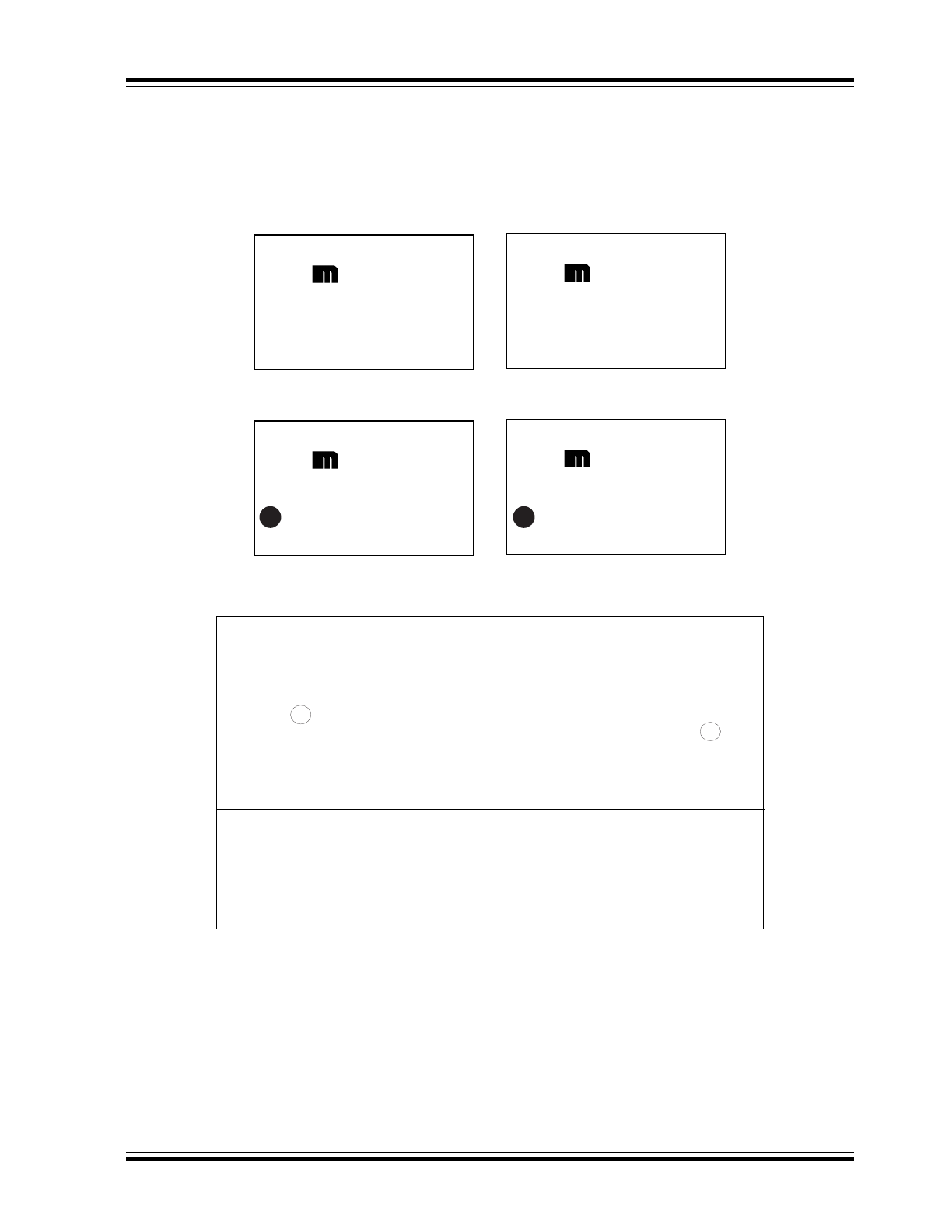
PACKAGING INFORMATION
5.1
Package Marking Information
16-Pin PDIP*
Example
XXXXXX
YYWW
XXXXXXXXX
MICREL
1312
MIC5891YN
16-Pin SOICW*
Example
XXXXXX
YYWW
XXXXXXXXXX
MICREL
1632
MIC5891YWM
Legend:
XX...X
Product code or customer-specific information
Y
Year code (last digit of calendar year)
YY
Year code (last 2 digits of calendar year)
WW
Week code (week of January 1 is week ‘01’)
NNN
Alphanumeric traceability code
Pb-free JEDEC
®
designator for Matte Tin (Sn)
*
This package is Pb-free. The Pb-free JEDEC designator ( )
can be found on the outer packaging for this package.
●, ▲, ▼ Pin one index is identified by a dot, delta up, or delta down (triangle
mark).
Note
:
In the event the full Microchip part number cannot be marked on one line, it will
be carried over to the next line, thus limiting the number of available
characters for customer-specific information. Package may or may not include
the corporate logo.
Underbar (_) and/or Overbar (⎯) symbol may not be to scale.
3
e
3
e
MIC5891
DS20005638A-page 10
2016 Microchip Technology Inc.
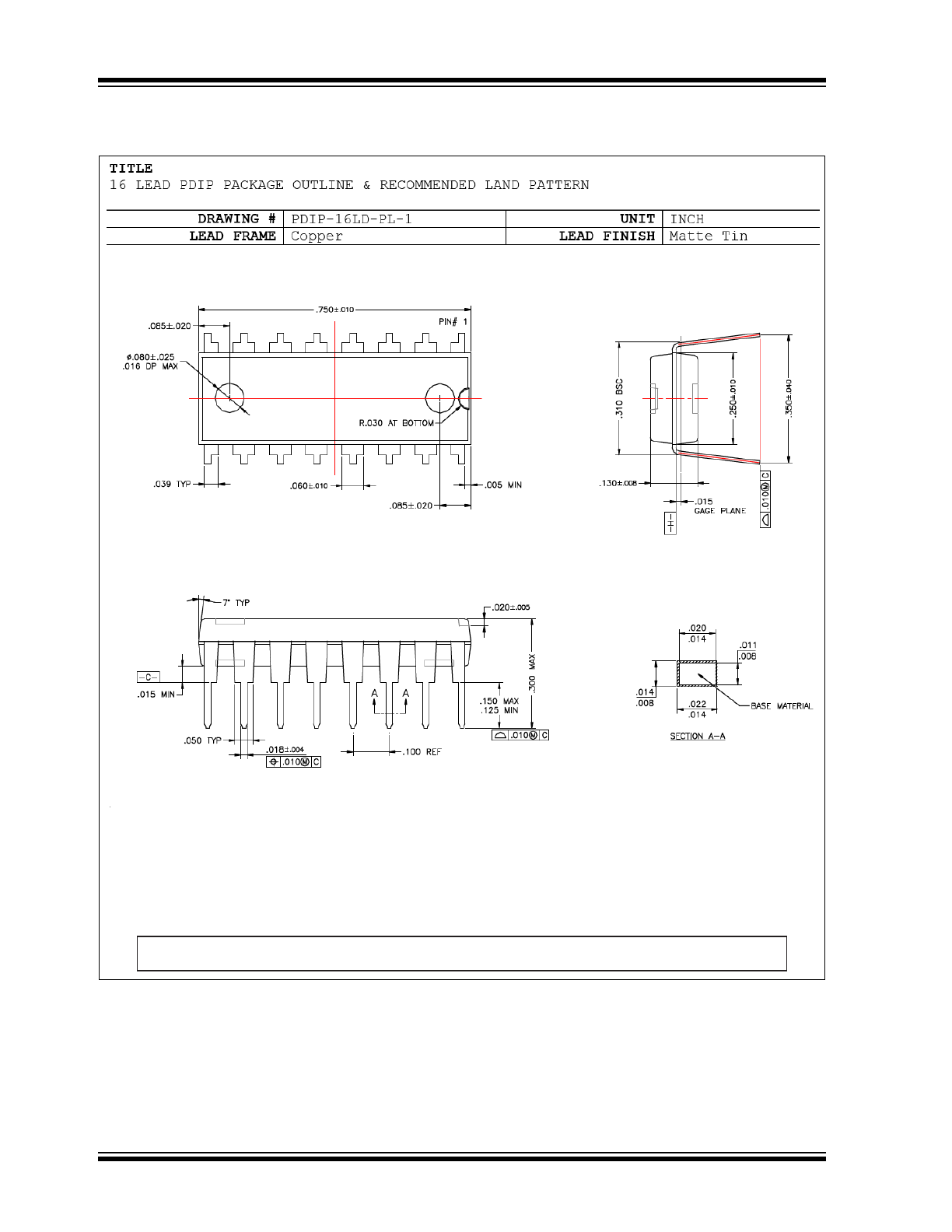
16-Lead PDIP Package Outline and Recommended Land Pattern
Note: For the most current package drawings, please see the Microchip Packaging Specification located at
http://www.microchip.com/packaging.