
© 2007 Microchip Technology Inc.
DS21919E-page 1
MCP23008/MCP23S08
Features
• 8-bit remote bidirectional I/O port
- I/O pins default to input
• High-speed I
2
C™ interface (MCP23008)
- 100 kHz
- 400 kHz
- 1.7 MHz
• High-speed SPI interface (MCP23S08)
- 10 MHz
• Hardware address pins
- Three for the MCP23008 to allow up to eight
devices on the bus
- Two for the MCP23S08 to allow up to four
devices using the same chip-select
• Configurable interrupt output pin
- Configurable as active-high, active-low or
open-drain
• Configurable interrupt source
- Interrupt-on-change from configured defaults
or pin change
• Polarity Inversion register to configure the polarity
of the input port data
• External reset input
• Low standby current: 1 µA (max.)
• Operating voltage:
- 1.8V to 5.5V @ -40°C to +85°C
I
2
C @ 100 kHz
SPI @ 5 MHz
- 2.7V to 5.5V @ -40°C to +85°C
I
2
C @ 400 kHz
SPI @ 10 MHz
- 4.5V to 5.5V @ -40°C to +125°C
I
2
C @ 1.7 kHz
SPI @ 10 MHz
Packages
• 18-pin PDIP (300 mil)
• 18-pin SOIC (300 mil)
• 20-pin SSOP
• 20-pin QFN
Block Diagram
GP0
GP1
GP2
GP3
GP4
GP5
GP6
GP7
Serial
Control
GPIO
SCL
SDA
RESET
INT
8
Configuration/
8
A2:A0
3
Control
Registers
Serializer/
Deserializer
Interrupt
Logic
V
DD
V
SS
POR
Decode
Interface
SCK
SI
SO
MCP23S08
MCP23008
A1:A0
MCP23S08
8-Bit I/O Expander with Serial Interface
MCP23008/MCP23S08
DS21919E-page 2
© 2007 Microchip Technology Inc.
Package Types
SDA
SCL
NC
INT
RESET
A1
GP4
V
DD
GP7
GP6
GP5
GP3
GP2
1
2
3
4
5
6
7
18
17
16
15
14
13
12
PDIP/SOIC
8
9
11
10
GP1
GP0
A0
A2
V
SS
MC
P2300
8
MCP23008
MCP23
008
13
12
1
2
3
4
5
6
7
8
9
20
19
18
17
16
15
14
11
10
GP3
V
DD
GP7
GP6
GP5
GP2
GP1
GP0
N/C
GP4
SDA
SCL
V
SS
A0
N/C
A1
RESET
A2
NC
INT
SSOP
MCP23008
20
19
18
17
16
6
7
8
9
10
15
14
13
12
11
1
2
3
4
5
QFN
SCL
SDA
V
SS
A0
N/C
A1
RESET
A2
NC
INT
GP3
V
DD
GP7
GP6
GP5
GP2
GP1
GP0
N/C
GP4
© 2007 Microchip Technology Inc.
DS21919E-page 3
MCP23008/MCP23S08
Package Types: (Continued)
SI
SCK
CS
INT
RESET
A1
GP4
V
DD
GP7
GP6
GP5
GP3
GP2
1
2
3
4
5
6
7
18
17
16
15
14
13
12
PDIP/SOIC
8
9
11
10
GP1
GP0
A0
SO
V
SS
MCP23S
08
MCP23S08
MCP23S08
13
12
1
2
3
4
5
6
7
8
9
20
19
18
17
16
15
14
11
10
GP3
V
DD
GP7
GP6
GP5
GP2
GP1
GP0
N/C
GP4
SI
SCK
V
SS
A0
N/C
A1
RESET
SO
CS
INT
SSOP
QFN
MCP23S08
20
19
18
17
16
6
7
8
9
10
15
14
13
12
11
1
2
3
4
5
SCK
SI
V
SS
A0
N/C
A1
RESET
A2
CS
INT
GP3
V
DD
GP7
GP6
GP5
GP2
GP1
GP0
N/C
GP4

MCP23008/MCP23S08
DS21919E-page 4
© 2007 Microchip Technology Inc.
NOTES:
© 2007 Microchip Technology Inc.
DS21919E-page 5
MCP23008/MCP23S08
1.0
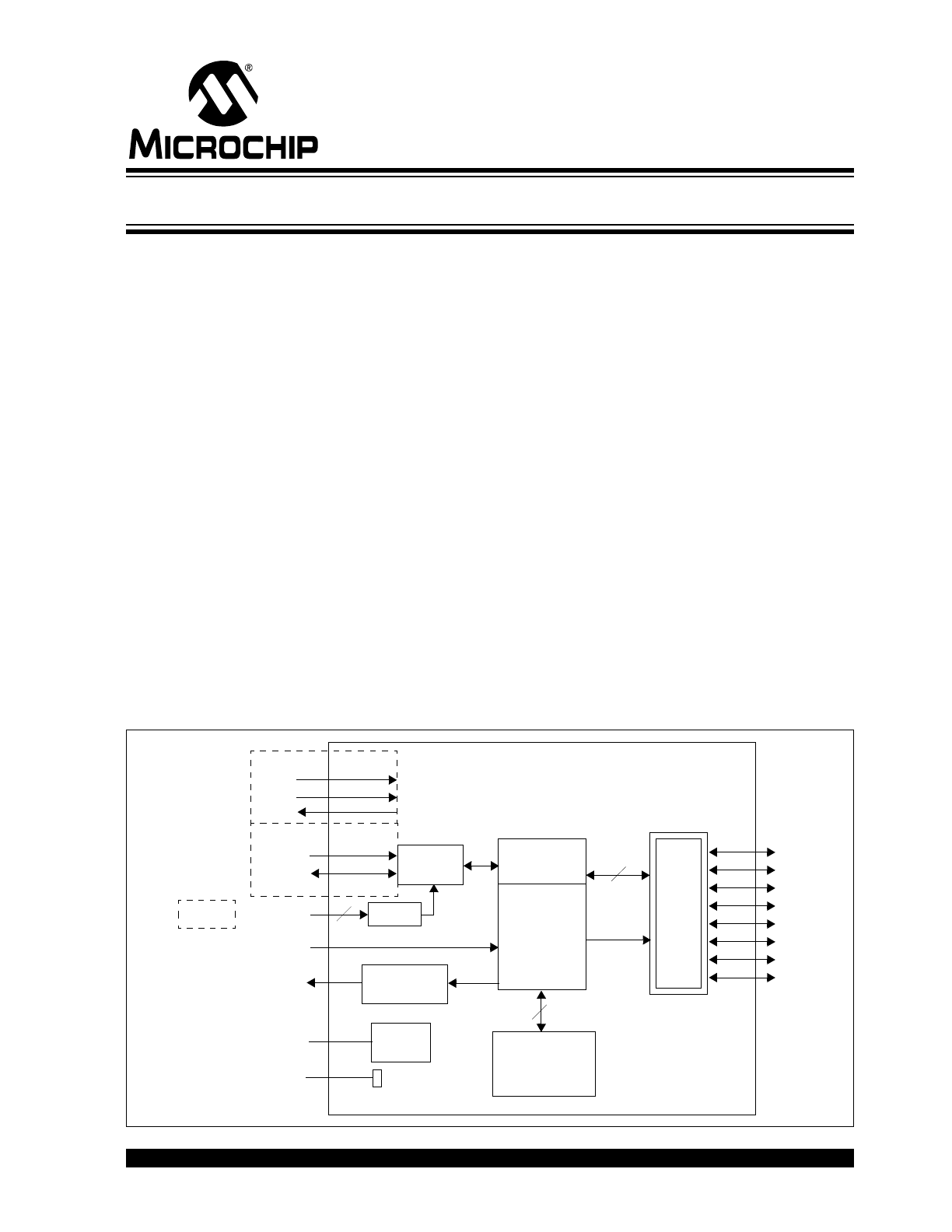
DEVICE OVERVIEW
The MCP23X08 device provides 8-bit, general
purpose, parallel I/O expansion for I
2
C bus or SPI
applications. The two devices differ in the number of
hardware address pins and the serial interface:
• MCP23008 – I
2
C interface; three address pins
• MCP23S08 – SPI interface; two address pins
The MCP23X08 consists of multiple 8-bit configuration
registers for input, output and polarity selection. The
system master can enable the I/Os as either inputs or
outputs by writing the I/O configuration bits. The data
for each input or output is kept in the corresponding
Input or Output register. The polarity of the Input Port
register can be inverted with the Polarity Inversion
register. All registers can be read by the system master.
The interrupt output can be configured to activate
under two conditions (mutually exclusive):
1.
When any input state differs from its
corresponding input port register state, this is
used to indicate to the system master that an
input state has changed.
2.
When an input state differs from a preconfigured
register value (DEFVAL register).
The Interrupt Capture register captures port values at
the time of the interrupt, thereby saving the condition
that caused the interrupt.
The Power-on Reset (POR) sets the registers to their
default values and initializes the device state machine.
The hardware address pins are used to determine the
device address.
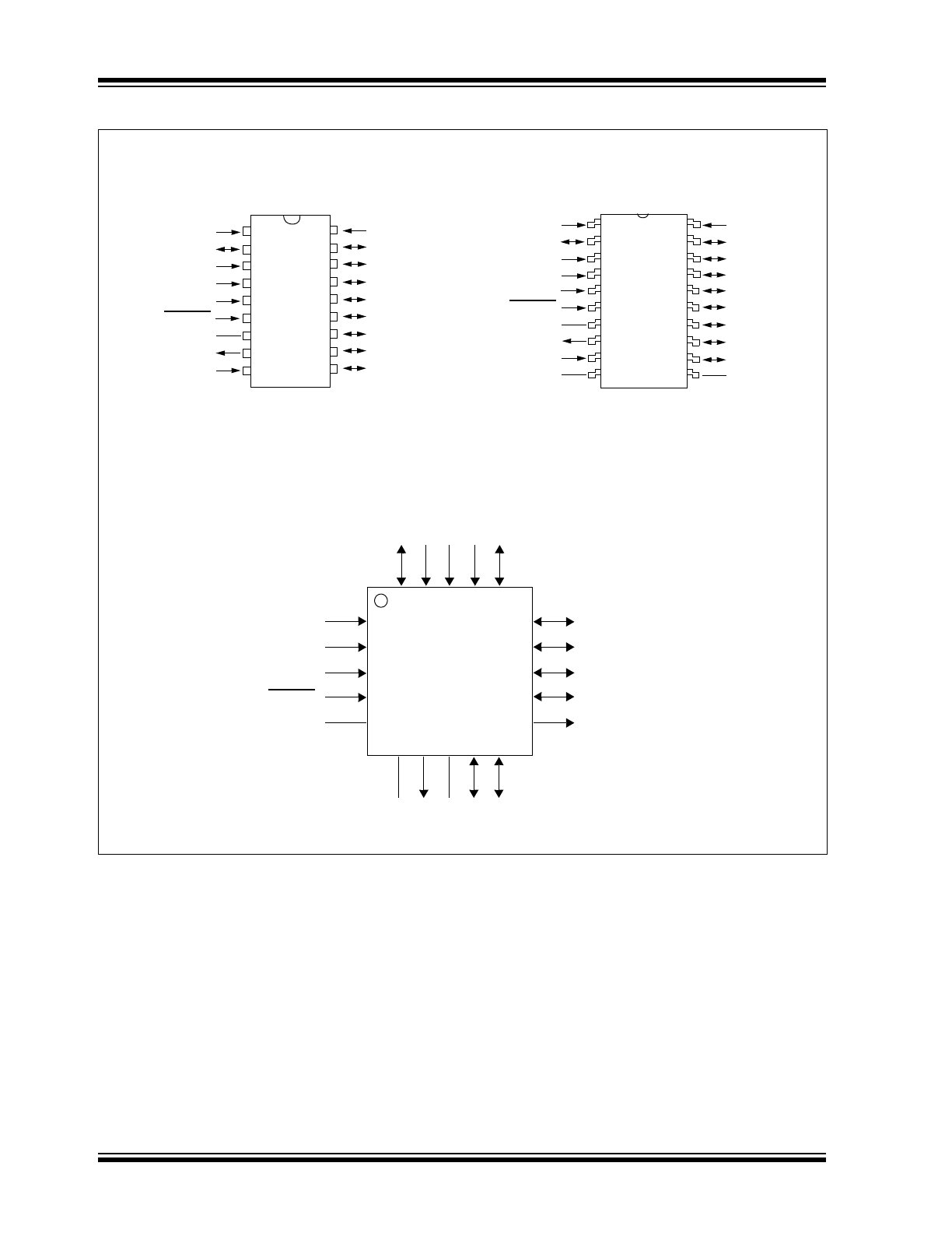
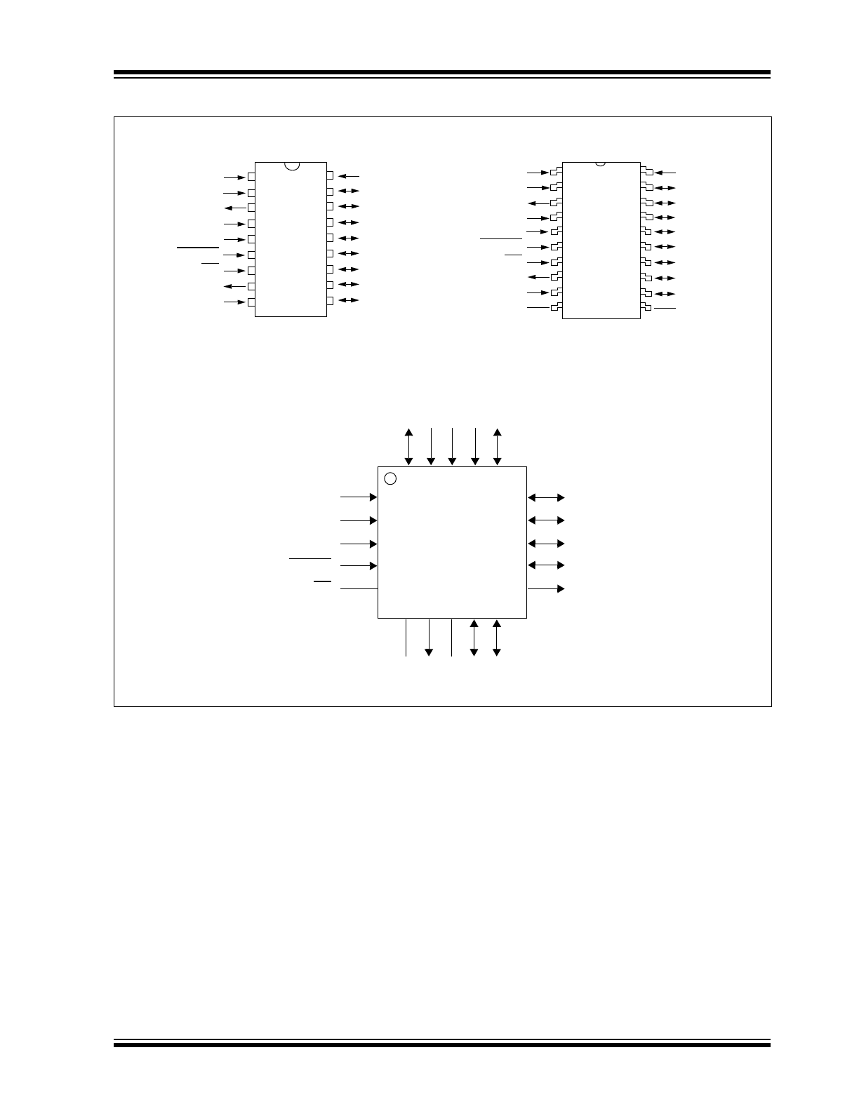
1.1
Pin Descriptions
TABLE 1-1:
PINOUT DESCRIPTION
Pin
Name
PDIP/
SOIC
QFN
SSOP
Pin
Type
Function
SCL/SCK
1
19
1
I
Serial clock input.
SDA/SI
2
20
2
I/O
Serial data I/O (MCP23008)/Serial data input (MCP23S08).
A2/SO
3
1
3
I/O
Hardware address input (MCP23008)/
Serial data output (MCP23S08).
A2 must be biased externally.
A1
4
2
4
I
Hardware address input. Must be biased externally.
A0
5
3
5
I
Hardware address input. Must be biased externally.
RESET
6
4
6
I
External reset input. Must be biased externally.
NC/CS
7
5
7
I
No connect (MCP23008)/External chip select input (MCP23S08).
INT
8
7
8
O
Interrupt output. Can be configured for active-high, active-low or
open-drain.
V
SS
9
17
9
P
Ground.
GP0
10
9
12
I/O
Bidirectional I/O pin. Can be enabled for interrupt-on-change and/or
internal weak pull-up resistor.
GP1
11
10
13
I/O
Bidirectional I/O pin. Can be enabled for interrupt-on-change and/or
internal weak pull-up resistor.
GP2
12
11
14
I/O
Bidirectional I/O pin. Can be enabled for interrupt-on-change and/or
internal weak pull-up resistor.
GP3
13
12
15
I/O
Bidirectional I/O pin. Can be enabled for interrupt-on-change and/or
internal weak pull-up resistor.
GP4
14
13
16
I/O
Bidirectional I/O pin. Can be enabled for interrupt-on-change and/or
internal weak pull-up resistor.
GP5
15
14
17
I/O
Bidirectional I/O pin. Can be enabled for interrupt-on-change and/or
internal weak pull-up resistor.
GP6
16
15
18
I/O
Bidirectional I/O pin. Can be enabled for interrupt-on-change and/or
internal weak pull-up resistor.
GP7
17
16
19
I/O
Bidirectional I/O pin. Can be enabled for interrupt-on-change and/or
internal weak pull-up resistor.
V
DD
18
18
20
P
Power.
N/C
—
6, 8
10, 11
—
—

MCP23008/MCP23S08
DS21919E-page 6
© 2007 Microchip Technology Inc.
1.2
Power-on Reset (POR)
The on-chip POR circuit holds the device in reset until
V
DD
has reached a high enough voltage to deactivate
the POR circuit (i.e., release the device from Reset).
The maximum V
DD
rise time is specified in Section 2.0
“Electrical Characteristics”.
When the device exits the POR condition (releases
reset), device operating parameters (i.e., voltage,
temperature, serial bus frequency, etc.) must be met to
ensure proper operation.
1.3
Serial Interface
This block handles the functionality of the I
2
C
(MCP23008) or SPI (MCP23S08) interface protocol.
The MCP23X08 contains eleven registers that can be
addressed through the serial interface block (Table 1-2):
TABLE 1-2:
REGISTER ADDRESSES
1.3.1
SEQUENTIAL OPERATION BIT
The Sequential Operation (SEQOP) bit (IOCON
register) controls the operation of the address pointer.
The address pointer can either be enabled (default) to
allow the address pointer to increment automatically
after each data transfer, or it can be disabled.
When operating in Sequential mode
(IOCON.SEQOP = 0), the address pointer automati-
cally increments to the next address after each byte
is clocked.
When operating in Byte mode (IOCON.SEQOP = 1),
the MCP23X08 does not increment its address
counter after each byte during the data transfer. This
gives the ability to continually read the same address
by providing extra clocks (without additional control
bytes). This is useful for polling the GPIO register for
data changes.
1.3.2
I
2
C™ INTERFACE
1.3.2.1
I
2
C Write Operation
The I
2
C Write operation includes the control byte and
register address sequence, as shown in the bottom of
Figure 1-1. This sequence is followed by eight bits of
data from the master and an Acknowledge (ACK) from
the MCP23008. The operation is ended with a STOP
or RESTART condition being generated by the master.
Data is written to the MCP23008 after every byte
transfer. If a STOP or RESTART condition is
generated during a data transfer, the data will not be
written to the MCP23008.
Byte writes and sequential writes are both supported
by the MCP23008. The MCP23008 increments its
address counter after each ACK during the data
transfer.
1.3.2.2
I
2
C Read Operation
The I
2
C Read operation includes the control byte
sequence, as shown in the bottom of Figure 1-1. This
sequence is followed by another control byte (includ-
ing the START condition and ACK) with the R/W bit
equal to a logic 1 (R/W = 1). The MCP23008 then
transmits the data contained in the addressed register.
The sequence is ended with the master generating a
STOP or RESTART condition.
1.3.2.3
I
2
C Sequential Write/Read
For sequential operations (Write or Read), instead of
transmitting a STOP or RESTART condition after the
data transfer, the master clocks the next byte pointed to
by the address pointer (see Section 1.3.1 “Sequential
Operation Bit” for details regarding sequential
operation control).
The sequence ends with the master sending a STOP or
RESTART condition.
The MCP23008 address pointer will roll over to
address zero after reaching the last register address.
Refer to Figure 1-1.
1.3.3
SPI INTERFACE
1.3.3.1
SPI Write Operation
The SPI Write operation is started by lowering CS. The
Write command (slave address with R/W bit cleared) is
then clocked into the device. The opcode is followed by
an address and at least one data byte.
1.3.3.2
SPI Read Operation
The SPI Read operation is started by lowering CS. The
SPI read command (slave address with R/W bit set) is
then clocked into the device. The opcode is followed by
an address, with at least one data byte being clocked
out of the device.
Address
Access to:
00h
IODIR
01h
IPOL
02h
GPINTEN
03h
DEFVAL
04h
INTCON
05h
IOCON
06h
GPPU
07h
INTF
08h
INTCAP (Read-only)
09h
GPIO
0Ah
OLAT
© 2007 Microchip Technology Inc.
DS21919E-page 7
MCP23008/MCP23S08
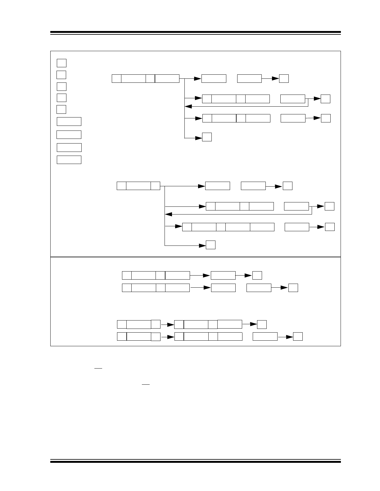
FIGURE 1-1:
MCP23008 I
2
C™ DEVICE PROTOCOL
1.3.3.3
SPI Sequential Write/Read
For sequential operations, instead of deselecting the
device by raising CS, the master clocks the next byte
pointed to by the address pointer.
The sequence ends by the raising of CS.
The MCP23S08 address pointer will roll over to
address zero after reaching the last register address.
1.4
Hardware Address Decoder
The hardware address pins are used to determine the
device address. To address a device, the correspond-
ing address bits in the control byte must match the pin
state.
• MCP23008 has address pins A2, A1 and A0.
• MCP23S08 has address pins A1 and A0.
The pins must be biased externally.
S
P
SR
w
R
OP
ADDR
D
OUT
D
IN
- START
- RESTART
- STOP
- Write
- Read
- Device opcode
- Device address
- Data out from MCP23008
- Data into MCP23008
S
P
SR
W
R
OP
ADDR
D
IN
D
IN
....
S
P
W
R
OP
ADDR
D
OUT
D
OUT
....
P
SR
W
OP
D
IN
D
IN
....
P
P
SR
R
D
OUT
D
OUT
....
P
OP
D
OUT
D
OUT
....
P
SR
OP
D
IN
....
P
OP
D
IN
S
P
W
OP
ADDR
D
IN
D
IN
....
Byte and Sequential Write
S
W
OP
SR
R
OP
D
OUT
D
OUT
....
P
Byte and Sequential Read
S
W
OP
ADDR
D
IN
P
S
W
OP
SR
R
OP
D
OUT
P
Byte
Sequential
Byte
Sequential
MCP23008/MCP23S08
DS21919E-page 8
© 2007 Microchip Technology Inc.
1.4.1
ADDRESSING I
2
C DEVICES
(MCP23008)
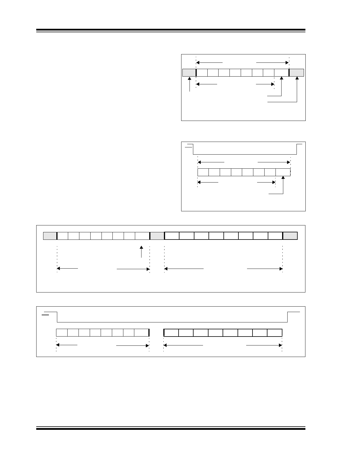
The MCP23008 is a slave I
2
C device that supports 7-bit
slave addressing, with the read/write bit filling out the
control byte. The slave address contains four fixed bits
and three user-defined hardware address bits (pins A2,
A1 and A0). Figure 1-2 shows the control byte format.
1.4.2
ADDRESSING SPI DEVICES
(MCP23S08)
The MCP23S08 is a slave SPI device. The slave
address contains five fixed bits and two user-defined
hardware address bits (pins A1 and A0), with the read/
write bit filling out the control byte. Figure 1-3 shows
the control byte format.
FIGURE 1-2:
I
2
C™ CONTROL BYTE
FORMAT
FIGURE 1-3:
SPI CONTROL BYTE
FORMAT
FIGURE 1-4:
I
2
C™ ADDRESSING REGISTERS
FIGURE 1-5:
SPI ADDRESSING REGISTERS
S
0
1
0
0
A2 A1 A0 R/W ACK
Start
bit
Slave Address
R/W bit
ACK bit
Control Byte
R/W = 0 = write
R/W = 1 = read
0
1
0
0
0
A1 A0 R/W
Slave Address
R/W bit
Control Byte
R/W = 0 = write
R/W = 1 = read
CS
S
0
1
0
0
A2 A1 A0
0
ACK
A7
A6
A5
A4
A3
A2
A1
A0
ACK
Device Opcode
Register Address
R/W = 0
The ACKs are provided by the MCP23008.
0
1
0
0
0
A1 A0 R/W
A7
A6
A5
A4
A3
A2
A1
A0
Device Opcode
Register Address
CS
© 2007 Microchip Technology Inc.
DS21919E-page 9
MCP23008/MCP23S08
1.5
GPIO Port
The GPIO module contains the data port (GPIO),
internal pull up resistors and the Output Latches
(OLAT).
Reading the GPIO register reads the value on the port.
Reading the OLAT register only reads the OLAT, not
the actual value on the port.
Writing to the GPIO register actually causes a write to
the OLAT. Writing to the OLAT register forces the
associated output drivers to drive to the level in OLAT.
Pins configured as inputs turn off the associated output
driver and put it in high-impedance.
1.6
Configuration and Control
Registers
The Configuration and Control blocks contain the
registers as shown in Table 1-3.
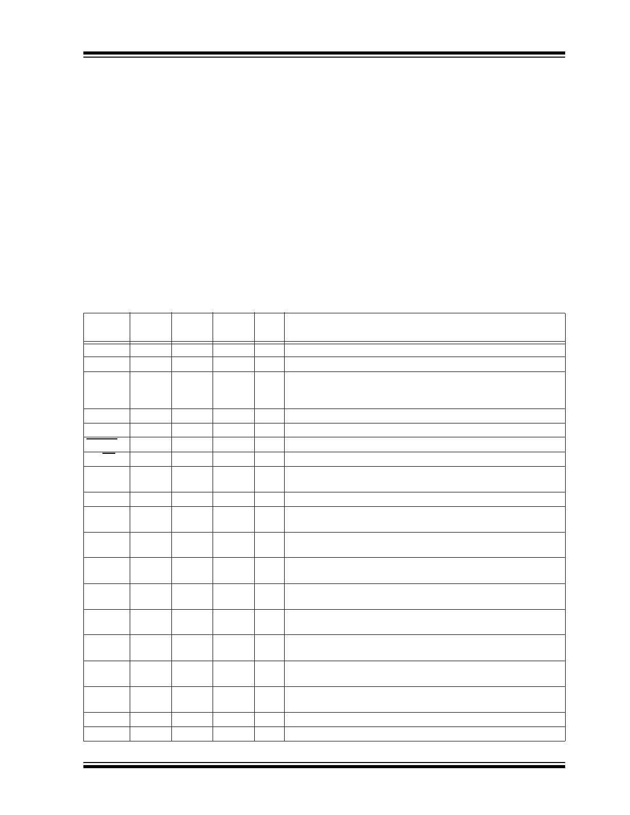
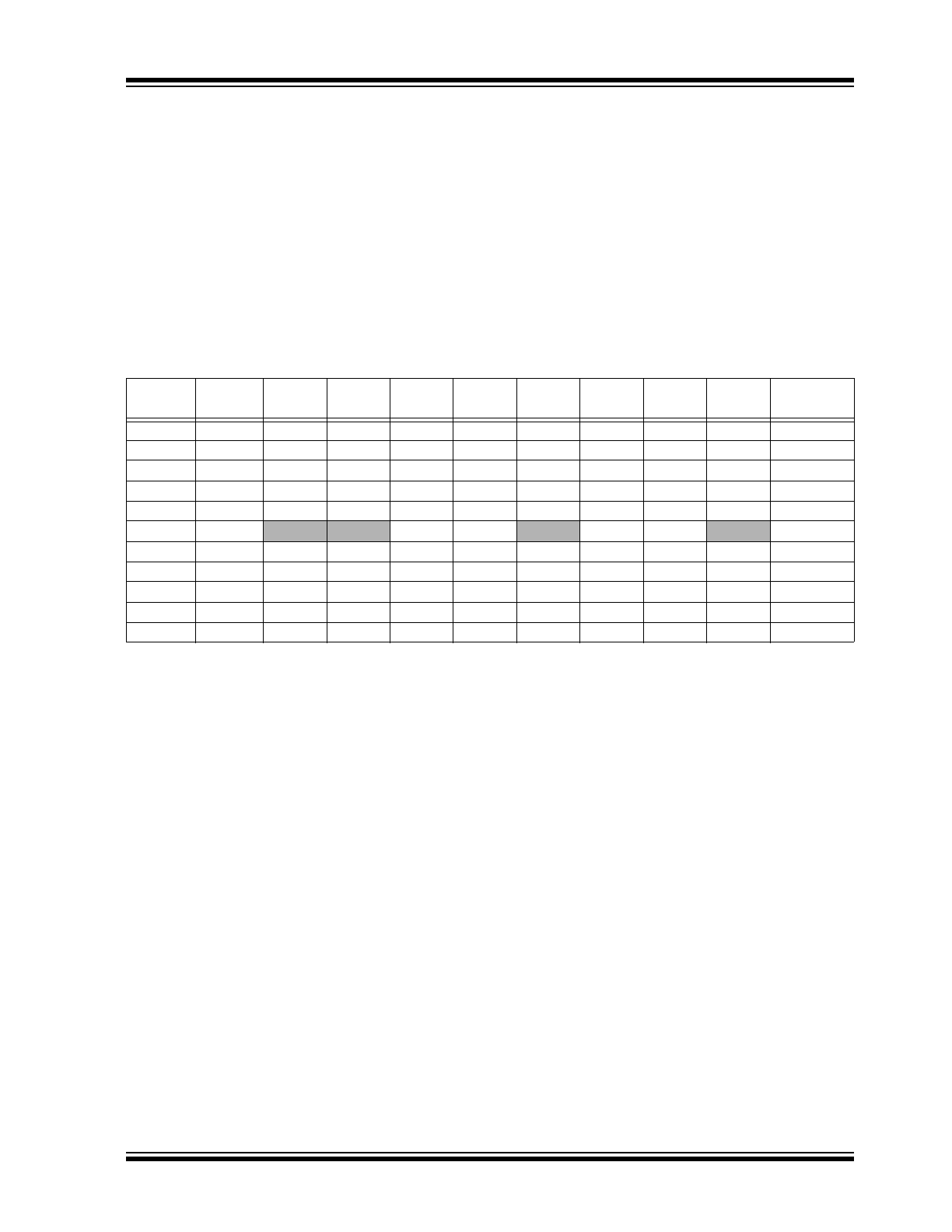
TABLE 1-3:
CONFIGURATION AND CONTROL REGISTERS
Register
Name
Address
(hex)
bit 7
bit 6
bit 5
bit 4
bit 3
bit 2
bit 1
bit 0
POR/RST
value
IODIR
00
IO7
IO6
IO5
IO4
IO3
IO2
IO1
IO0
1111 1111
IPOL
01
IP7
IP6
IP5
IP4
IP3
IP2
IP1
IP0
0000 0000
GPINTEN
02
GPINT7
GPINT6
GPINT5
GPINT4
GPINT3
GPINT2
GPINT1
GPINT0
0000 0000
DEFVAL
03
DEF7
DEF6
DEF5
DEF4
DEF3
DEF2
DEF1
DEF0
0000 0000
INTCON
04
IOC7
IOC6
IOC5
IOC4
IOC3
IOC2
IOC1
IOC0
0000 0000
IOCON
05
—
—
SREAD
DISSLW
HAEN*
ODR
INTPOL
—
--00 000-
GPPU
06
PU7
PU6
PU5
PU4
PU3
PU2
PU1
PU0
0000 0000
INTF
07
INT7
INT6
INT5
INT4
INT3
INT2
INT1
INTO
0000 0000
INTCAP
08
ICP7
ICP6
ICP5
ICP4
ICP3
ICP2
ICP1
ICP0
0000 0000
GPIO
09
GP7
GP6
GP5
GP4
GP3
GP2
GP1
GP0
0000 0000
OLAT
0A
OL7
OL6
OL5
OL4
OL3
OL2
OL1
OL0
0000 0000
* Not used on the MCP23008.
MCP23008/MCP23S08
DS21919E-page 10
© 2007 Microchip Technology Inc.
1.6.1
I/O DIRECTION (IODIR) REGISTER
Controls the direction of the data I/O.
When a bit is set, the corresponding pin becomes an
input. When a bit is clear, the corresponding pin
becomes an output.
REGISTER 1-1:
IODIR – I/O DIRECTION REGISTER (ADDR 0x00)
R/W-1
R/W-1
R/W-1
R/W-1
R/W-1
R/W-1
R/W-1
R/W-1
IO7
IO6
IO5
IO4
IO3
IO2
IO1
IO0
bit 7
bit 0
Legend:
R = Readable bit
W = Writable bit
U = Unimplemented bit, read as ‘0’
-n = Value at POR
‘1’ = Bit is set
‘0’ = Bit is cleared
x = Bit is unknown
bit 7-0
IO7:IO0: These bits control the direction of data I/O <7:0>
1 = Pin is configured as an input.
0 = Pin is configured as an output.