

Features
•
High performance, low power AVR
®
8-bit Microcontroller
•
Advanced RISC architecture
– 135 powerful instructions – most single clock cycle execution
– 32 × 8 general purpose working registers
– Fully static operation
– Up to 16MIPS throughput at 16MHz
– On-chip 2-cycle multiplier
•
Non-volatile program and data memories
– 64/128Kbytes of in-system self-programmable flash
• Endurance: 100,000 write/erase cycles
– Optional Boot Code section with independent lock bits
• USB boot loader programmed by default in the factory
• In-system programming by on-chip boot program hardware activated after
reset
• True read-while-write operation
• All supplied parts are pre-programed with a default USB bootloader
– 2K/4K (64K/128K flash version) bytes EEPROM
• Endurance: 100,000 write/erase cycles
– 4K/8K (64K/128K flash version) bytes internal SRAM
– Up to 64Kbytes optional external memory space
– Programming lock for software security
•
JTAG (IEEE std. 1149.1 compliant) interface
– Boundary-scan capabilities according to the JTAG standard
– Extensive on-chip debug support
– Programming of flash, EEPROM, fuses, and lock bits through the JTAG interface
•
USB 2.0 full-speed/low-speed device and on-the-go module
– Complies fully with:
– Universal serial bus specification REV 2.0
– On-the-go supplement to the USB 2.0 specification rev 1.0
– Supports data transfer rates up to 12Mbit/s and 1.5Mbit/s
•
USB full-speed/low speed device module with interrupt on transfer completion
– Endpoint 0 for control transfers: up to 64-bytes
– Six programmable endpoints with in or out directions and with bulk, interrupt or
isochronous transfers
– Configurable endpoints size up to 256bytes in double bank mode
– Fully independent 832bytes USB DPRAM for endpoint memory allocation
– Suspend/resume interrupts
– Power-on reset and USB bus reset
– 48MHz PLL for full-speed bus operation
– USB bus disconnection on microcontroller request
•
USB OTG reduced host:
– Supports host negotiation protocol (HNP) and session request protocol (SRP) for
OTG dual-role devices
– Provide status and control signals for software implementation of HNP and SRP
– Provides programmable times required for HNP and SRP
•
Peripheral features
– Two 8-bit timer/counters with separate prescaler and compare mode
– Two16-bit timer/counter with separate prescaler, compare- and capture mode
8-bit Atmel
Microcontroller
with
64/128Kbytes
of ISP Flash
and USB
Controller
AT90USB646
AT90USB647
AT90USB1286
AT90USB1287
7593LS–AVR–09/12

2
7593LS–AVR–09/12
AT90USB64/128
– Real time counter with separate oscillator
– Four 8-bit PWM channels
– Six PWM channels with programmable resolution from 2 to 16 bits
– Output compare modulator
– 8-channels, 10-bit ADC
– Programmable serial USART
– Master/slave SPI serial interface
– Byte oriented 2-wire serial interface
– Programmable watchdog timer with separate on-chip oscillator
– On-chip analog comparator
– Interrupt and wake-up on pin change
•
Special microcontroller features
– Power-on reset and programmable brown-out detection
– Internal calibrated oscillator
– External and internal interrupt sources
– Six sleep modes: Idle, ADC Noise Reduction, Power-save, Power-down, Standby, and Extended Standby
•
I/O and packages
– 48 programmable I/O lines
– 64-lead TQFP and 64-lead QFN
•
Operating voltages
– 2.7 - 5.5V
•
Operating temperature
– Industrial (-40°C to +85°C)
•
Maximum frequency
– 8MHz at 2.7V - industrial range
– 16MHz at 4.5V - industrial range

3
7593LS–AVR–09/12
AT90USB64/128
1.
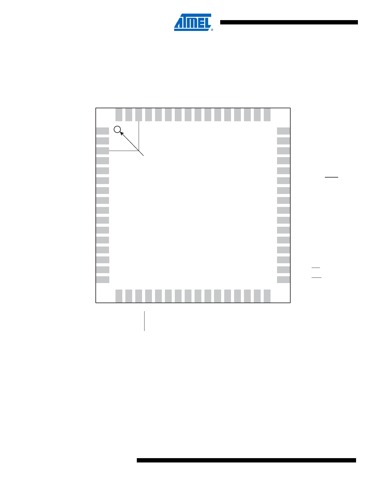
Pin configurations
Figure 1-1.
Pinout Atmel AT90USB64/128-TQFP.
AT90USB90128/64
TQFP64
(INT.7/AIN.1/UVcon) PE7
UVcc
D-
D+
UGnd
UCap
VBus
(IUID) PE3
(SS/PCINT0) PB0
(INT.6/AIN.0) PE6
(PCINT1/SCLK) PB1
(PDI/PCINT2/MOSI) PB2
(PDO/PCINT3/MISO) PB3
(PCINT4/OC.2A) PB4
(PCINT5/OC.1A) PB5
(PCINT6/OC.1B) PB6
(PCINT7/OC
.0A/OC
.1C) PB7
(INT4/T
OSC1) PE4
(INT
.5/T
OSC2) PE5
RESET
VCC
GND
XT
AL2
XT
AL1
(OC0B/SCL/INT0) PD0
(OC2B/SD
A/INT1) PD1
(RXD1/INT2) PD2
(TXD1/INT3) PD3
(ICP1) PD4
(XCK1) PD5
PA3 (AD3)
PA4 (AD4)
PA5 (AD5)
PA6 (AD6)
PA7 (AD7)
PE2 (ALE/HWB)
PC7 (A15/IC.3/CLKO)
PC6 (A14/OC.3A)
PC5 (A13/OC.3B)
PC4 (A12/OC.3C)
PC3 (A11/T.3)
PC2 (A10)
PC1 (A9)
PC0 (A8)
PE1 (RD)
PE0 (WR)
A
VCC
GND
AREF
PF0 (ADC0)
PF1 (ADC1)
PF2 (ADC2)
PF3 (ADC3)
PF4 (ADC4/TCK)
PF5 (ADC5/TMS)
PF6 (ADC6/TDO)
PF7 (ADC7/TDI)
GND
VCC
P
A0 (AD0)
P
A1 (AD1)
P
A2 (AD2)
(T1) PD6
(T0) PD7
INDEX CORNER
1
2
3
4
5
6
7
8
9
10
11
12
13
14
15
16
64
63
62
61
60
59
58
57
56
55
54
53
52
51
50
49
48
47
46
45
44
43
42
41
40
39
38
37
36
35
34
33
17
18
19
20
21
22
23
24
25
26
27
28
29
30
31
32
4
7593LS–AVR–09/12
AT90USB64/128
Figure 1-2.
Pinout Atmel AT90USB64/128-QFN.
Note:
The large center pad underneath the MLF packages is made of metal and internally connected to
GND. It should be soldered or glued to the board to ensure good mechanical stability. If the center
pad is left unconnected, the package might loosen from the board.
2
3
1
4
5
6
7
8
9
10
11
12
13
14
16
33
15
47
46
48
45
44
43
42
41
40
39
38
37
36
35
34
17
18
20
19
21
22
23
24
25
26
27
29
28
32
31
30
52
51
50
49
64
63
62
53
61
60
59
58
57
56
55
54
AT90USB128/64
(64-lead QFN top view)
INDEX CORNER
A
V
CC
G
N
D
AREF
PF0 (ADC0)
PF1 (ADC1)
PF2 (ADC2)
PF3 (ADC3)
PF4 (ADC4/TCK)
PF5 (ADC5/TMS)
PF6 (ADC6/TDO)
PF7 (ADC7/TDI)
G
N
D
V
CC
P
A0 (AD0)
P
A1 (AD1)
P
A2 (AD2)
(INT.7/AIN.1/UVcon) PE7
UVcc
D-
D+
UGnd
UCap
VBus
(IUID) PE3
(SS/PCINT0) PB0
(INT.6/AIN.0) PE6
(PCINT1/SCLK) PB1
(PDI/PCINT2/MOSI) PB2
(PDO/PCINT3/MISO) PB3
(PCINT4/OC.2A) PB4
(PCINT5/OC.1A) PB5
(PCINT6/OC.1B) PB6
(PCI
N
T7/OC
.0A/OC
.1C) PB7
(I
N
T4/T
OSC1) PE4
(I
N
T
.5/T
OSC2) PE5
V
CC
G
N
D
XT
AL2
XT
AL1
(OC0B/SCL/I
N
T0) PD0
(OC2B/SD
A/I
N
T1) PD1
(RXD1/I
N
T2) PD2
(TXD1/I
N
T3) PD3
(ICP1) PD4
(XCK1) PD5
(T1) PD6
(T0) PD7
RESET
PA3 (AD3)
PA4 (AD4)
PA5 (AD5)
PA6 (AD6)
PA7 (AD7)
PE2 (ALE/HWB)
PC7 (A15/IC.3/CLKO)
PC6 (A14/OC.3A)
PC5 (A13/OC.3B)
PC4 (A12/OC.3C)
PC3 (A11/T.3)
PC2 (A10)
PC1 (A9)
PC0 (A8)
PE1 (RD)
PE0 (WR)

5
7593LS–AVR–09/12
AT90USB64/128
2.
Overview
The Atmel
®
AVR
®
AT90USB64/128 is a low-power CMOS 8-bit microcontroller based on the
Atmel
®
AVR
®
enhanced RISC architecture. By executing powerful instructions in a single clock
cycle, the AT90USB64/128 achieves throughputs approaching 1MIPS per MHz allowing the sys-
tem designer to optimize power consumption versus processing speed.
6
7593LS–AVR–09/12
AT90USB64/128
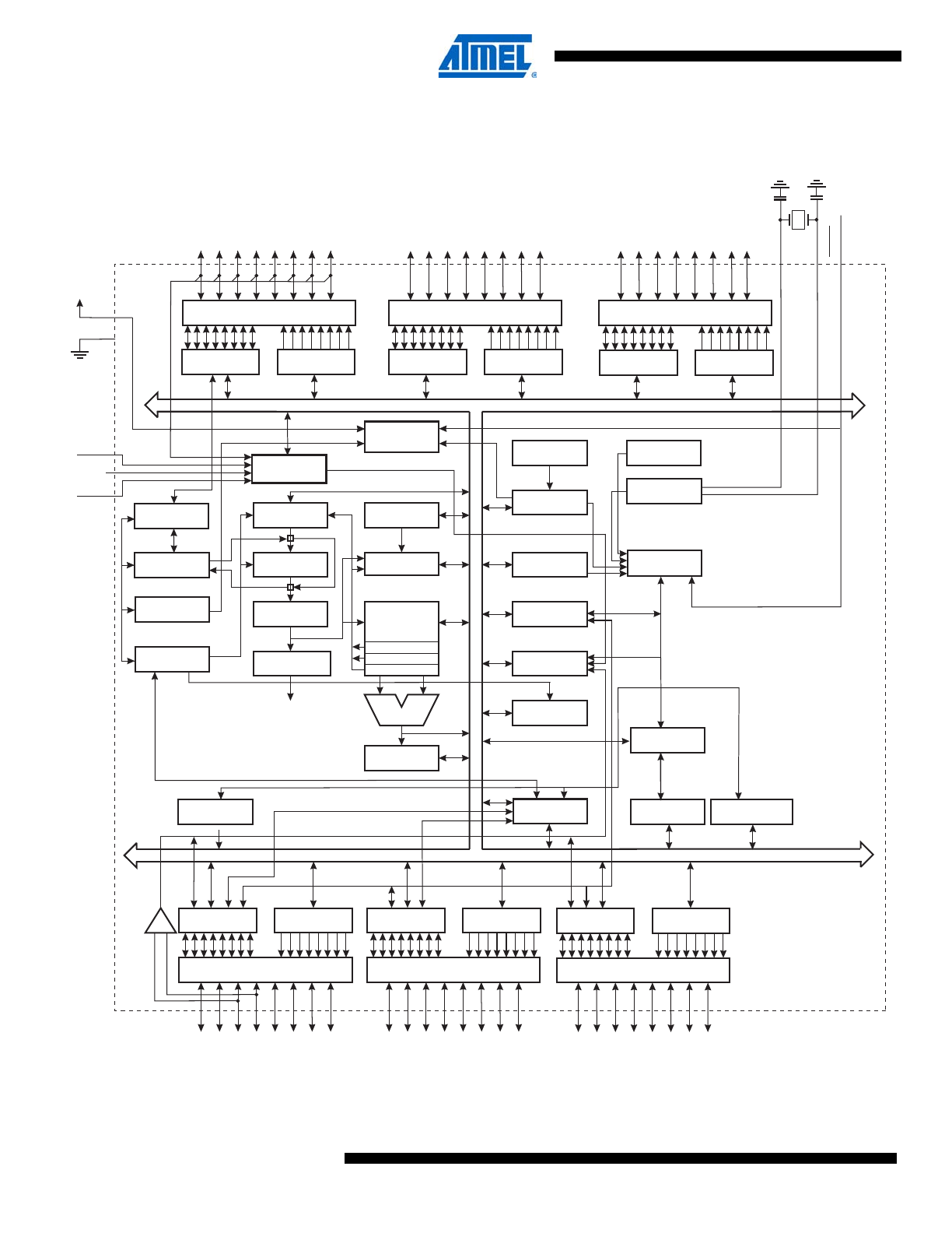
2.1
Block diagram
Figure 2-1.
Block diagram.
The AVR core combines a rich instruction set with 32 general purpose working registers. All the
32 registers are directly connected to the Arithmetic Logic Unit (ALU), allowing two independent
registers to be accessed in one single instruction executed in one clock cycle. The resulting
PROGRAM
COUNTER
ST ACK
POINTER
PROGRAM
FLASH
MCU CONTROL
REGISTER
SRAM
GENERAL
PURPOSE
REGISTERS
INSTRUCTION
REGISTER
TIMER/
COUNTERS
INSTRUCTION
DECODER
DATA DIR.
REG. PORTB
DATA DIR.
REG. PORTE
DATA DIR.
REG. PORT A
DATA DIR.
REG. PORTD
DATA REGISTER
PORTB
DATA REGISTER
PORTE
DATA REGISTER
PORT A
DAT A REGISTER
PORTD
INTERRUPT
UNIT
EEPROM
SPI
USART1
ST ATUS
REGISTER
Z
Y
X
ALU
POR TB DRIVERS
POR TE DRIVERS
POR TA DRIVERS
POR TF DRIVERS
POR TD DRIVERS
POR TC DRIVERS
PB7 - PB0
PE7 - PE0
PA7 - P A0
PF7 - PF0
RESE
T
VCC
AGND
GND
AREF
X
T
AL1
X
T
AL2
CONTROL
LINES
+
-
ANAL
OG
C
O
MP
ARA
T
OR
PC7 - PC0
INTERNAL
OSCILLA TOR
WATCHDOG
TIMER
8-BIT DA TA BUS
AVCC
USB
TIMING AND
CONTROL
OSCILLA TOR
CALIB. OSC
DATA DIR.
REG. PORT C
DATA REGISTER
PORT C
ON-CHIP DEBUG
JTAG TAP
PROGRAMMING
LOGIC
BOUNDARY-
SCAN
DATA DIR.
REG. PORT F
DATA REGISTER
PORT F
ADC
POR - BOD
RESET
PD7 - PD0
TWO-WIRE SERIAL
INTERFACE
PLL

7
7593LS–AVR–09/12
AT90USB64/128
architecture is more code efficient while achieving throughputs up to ten times faster than con-
ventional CISC microcontrollers.
The Atmel AT90USB64/128 provides the following features: 64/128Kbytes of In-System Pro-
grammable Flash with Read-While-Write capabilities, 2K/4Kbytes EEPROM, 4K/8K bytes
SRAM, 48 general purpose I/O lines, 32 general purpose working registers, Real Time Counter
(RTC), four flexible Timer/Counters with compare modes and PWM, one USART, a byte ori-
ented 2-wire Serial Interface, a 8-channels, 10-bit ADC with optional differential input stage with
programmable gain, programmable Watchdog Timer with Internal Oscillator, an SPI serial port,
IEEE std. 1149.1 compliant JTAG test interface, also used for accessing the On-chip Debug sys-
tem and programming and six software selectable power saving modes. The Idle mode stops
the CPU while allowing the SRAM, Timer/Counters, SPI port, and interrupt system to continue
functioning. The Power-down mode saves the register contents but freezes the Oscillator, dis-
abling all other chip functions until the next interrupt or Hardware Reset. In Power-save mode,
the asynchronous timer continues to run, allowing the user to maintain a timer base while the
rest of the device is sleeping. The ADC Noise Reduction mode stops the CPU and all I/O mod-
ules except Asynchronous Timer and ADC, to minimize switching noise during ADC
conversions. In Standby mode, the Crystal/Resonator Oscillator is running while the rest of the
device is sleeping. This allows very fast start-up combined with low power consumption. In
Extended Standby mode, both the main Oscillator and the Asynchronous Timer continue to run.
The device is manufactured using the Atmel high-density nonvolatile memory technology. The
On-chip ISP Flash allows the program memory to be reprogrammed in-system through an SPI
serial interface, by a conventional nonvolatile memory programmer, or by an On-chip Boot pro-
gram running on the AVR core. The boot program can use any interface to download the
application program in the application Flash memory. Software in the Boot Flash section will
continue to run while the Application Flash section is updated, providing true Read-While-Write
operation. By combining an 8-bit RISC CPU with In-System Self-Programmable Flash on a
monolithic chip, the AT90USB64/128 is a powerful microcontroller that provides a highly flexible
and cost effective solution to many embedded control applications.
The AT90USB64/128 AVR is supported with a full suite of program and system development
tools including: C compilers, macro assemblers, program debugger/simulators, in-circuit emula-
tors, and evaluation kits.

8
7593LS–AVR–09/12
AT90USB64/128
2.2
Pin descriptions
2.2.1
VCC
Digital supply voltage.
2.2.2
GND
Ground.
2.2.3
AVCC
Analog supply voltage.
2.2.4
Port A (PA7..PA0)
Port A is an 8-bit bidirectional I/O port with internal pull-up resistors (selected for each bit). The
Port A output buffers have symmetrical drive characteristics with both high sink and source
capability. As inputs, Port A pins that are externally pulled low will source current if the pull-up
resistors are activated. The Port A pins are tri-stated when a reset condition becomes active,
even if the clock is not running.
Port A also serves the functions of various special features of the Atmel AT90USB64/128 as
listed on
page 78
.
2.2.5
Port B (PB7..PB0)
Port B is an 8-bit bidirectional I/O port with internal pull-up resistors (selected for each bit). The
Port B output buffers have symmetrical drive characteristics with both high sink and source
capability. As inputs, Port B pins that are externally pulled low will source current if the pull-up
resistors are activated. The Port B pins are tri-stated when a reset condition becomes active,
even if the clock is not running.
Port B has better driving capabilities than the other ports.
Port B also serves the functions of various special features of the AT90USB64/128 as listed on
page 79
.
2.2.6
Port C (PC7..PC0)
Port C is an 8-bit bidirectional I/O port with internal pull-up resistors (selected for each bit). The
Port C output buffers have symmetrical drive characteristics with both high sink and source
capability. As inputs, Port C pins that are externally pulled low will source current if the pull-up
resistors are activated. The Port C pins are tri-stated when a reset condition becomes active,
even if the clock is not running.
Port C also serves the functions of special features of the AT90USB64/128 as listed on
page 82
.
2.2.7
Port D (PD7..PD0)
Port D is an 8-bit bi-directional I/O port with internal pull-up resistors (selected for each bit). The
Port D output buffers have symmetrical drive characteristics with both high sink and source
capability. As inputs, Port D pins that are externally pulled low will source current if the pull-up
resistors are activated. The Port D pins are tri-stated when a reset condition becomes active,
even if the clock is not running.
Port D also serves the functions of various special features of the AT90USB64/128 as listed on
page 83
.

9
7593LS–AVR–09/12
AT90USB64/128
2.2.8
Port E (PE7..PE0)
Port E is an 8-bit bidirectional I/O port with internal pull-up resistors (selected for each bit). The
Port E output buffers have symmetrical drive characteristics with both high sink and source
capability. As inputs, Port E pins that are externally pulled low will source current if the pull-up
resistors are activated. The Port E pins are tri-stated when a reset condition becomes active,
even if the clock is not running.
Port E also serves the functions of various special features of the AT90USB64/128 as listed on
page 86
.
2.2.9
Port F (PF7..PF0)
Port F serves as analog inputs to the A/D Converter.
Port F also serves as an 8-bit bidirectional I/O port, if the A/D Converter is not used. Port pins
can provide internal pull-up resistors (selected for each bit). The Port F output buffers have sym-
metrical drive characteristics with both high sink and source capability. As inputs, Port F pins
that are externally pulled low will source current if the pull-up resistors are activated. The Port F
pins are tri-stated when a reset condition becomes active, even if the clock is not running. If the
JTAG interface is enabled, the pull-up resistors on pins PF7(TDI), PF5(TMS), and PF4(TCK) will
be activated even if a reset occurs.
Port F also serves the functions of the JTAG interface.
2.2.10
D-
USB Full speed / Low Speed Negative Data Upstream Port. Should be connected to the USB D-
connector pin with a serial 22
Ω resistor.
2.2.11
D+
USB Full speed / Low Speed Positive Data Upstream Port. Should be connected to the USB D+
connector pin with a serial 22
Ω resistor.
2.2.12
UGND
USB Pads Ground.
2.2.13
UVCC
USB Pads Internal Regulator Input supply voltage.
2.2.14
UCAP
USB Pads Internal Regulator Output supply voltage. Should be connected to an external capac-
itor (1µF).
2.2.15
VBUS
USB VBUS monitor and OTG negociations.
2.2.16
RESET
Reset input. A low level on this pin for longer than the minimum pulse length will generate a
reset, even if the clock is not running. The minimum pulse length is given in
Table 9-1 on page
58
. Shorter pulses are not guaranteed to generate a reset.
2.2.17
XTAL1
Input to the inverting Oscillator amplifier and input to the internal clock operating circuit.

10
7593LS–AVR–09/12
AT90USB64/128
2.2.18
XTAL2
Output from the inverting oscillator amplifier.
2.2.19
AVCC
AVCC is the supply voltage pin for Port F and the A/D Converter. It should be externally con-
nected to V
CC
, even if the ADC is not used. If the ADC is used, it should be connected to V
CC
through a low-pass filter.
2.2.20
AREF
This is the analog reference pin for the A/D Converter.
3.
Resources
A comprehensive set of development tools, application notes and datasheets are available for
download on
http://www.atmel.com/avr
.
4.
About code examples
This documentation contains simple code examples that briefly show how to use various parts of
the device. Be aware that not all C compiler vendors include bit definitions in the header files
and interrupt handling in C is compiler dependent. Please confirm with the C compiler documen-
tation for more details.
These code examples assume that the part specific header file is included before compilation.
For I/O registers located in extended I/O map, "IN", "OUT", "SBIS", "SBIC", "CBI", and "SBI"
instructions must be replaced with instructions that allow access to extended I/O. Typically
"LDS" and "STS" combined with "SBRS", "SBRC", "SBR", and "CBR".