

Features
•
High Performance, Low Power AVR
®
8-Bit Microcontroller
•
Advanced RISC Architecture
– 125 Powerful Instructions – Most Single Clock Cycle Execution
– 32 x 8 General Purpose Working Registers
– Fully Static Operation
– Up to 16 MIPS Throughput at 16 MHz
•
Non-volatile Program and Data Memories
– 8K / 16K Bytes of In-System Self-Programmable Flash
• Endurance: 10,000 Write/Erase Cycles
– Optional Boot Code Section with Independent Lock Bits
• USB boot-loader programmed by default in the factory
• In-System Programming by on-chip Boot Program hardware-activated after
reset
• True Read-While-Write Operation
– 512 Bytes EEPROM
• Endurance: 100,000 Write/Erase Cycles
– 512 Bytes Internal SRAM
– Programming Lock for Software Security
•
USB 2.0 Full-speed Device Module with Interrupt on Transfer Completion
– Complies fully with Universal Serial Bus Specification REV 2.0
– 48 MHz PLL for Full-speed Bus Operation : data transfer rates at 12 Mbit/s
– Fully independant 176 bytes USB DPRAM for endpoint memory allocation
– Endpoint 0 for Control Transfers: from 8 up to 64-bytes
– 4 Programmable Endpoints:
• IN or Out Directions
• Bulk, Interrupt and IsochronousTransfers
• Programmable maximum packet size from 8 to 64 bytes
• Programmable single or double buffer
– Suspend/Resume Interrupts
– Microcontroller reset on USB Bus Reset without detach
– USB Bus Disconnection on Microcontroller Request
– USB pad multiplexed with PS/2 peripheral for single cable capability
•
Peripheral Features
– PS/2 compliant pad
– One 8-bit Timer/Counters with Separate Prescaler and Compare Mode (two 8-bit
PWM channels)
– One 16-bit Timer/Counter with Separate Prescaler, Compare and Capture Mode
(three 8-bit PWM channels)
– USART with SPI master only mode and hardware flow control (RTS/CTS)
– Master/Slave SPI Serial Interface
– Programmable Watchdog Timer with Separate On-chip Oscillator
– On-chip Analog Comparator
– Interrupt and Wake-up on Pin Change
•
On Chip Debug Interface (debugWIRE)
•
Special Microcontroller Features
– Power-On Reset and Programmable Brown-out Detection
– Internal Calibrated Oscillator
– External and Internal Interrupt Sources
8-bit
Microcontroller
with
8/16K Bytes of
ISP Flash
and USB
Controller
AT90USB82
AT90USB162
Summary
7707FS–AVR–11/10

2
7707FS–AVR–11/10
AT90USB82/162
– Five Sleep Modes: Idle, Power-save, Power-down, Standby, and Extended Standby
•
I/O and Packages
– 22 Programable I/O Lines
– QFN32 (5x5mm) / TQFP32 packages
•
Operating Voltages
– 2.7 - 5.5V
•
Operating temperature
– Industrial (-40°C to +85°C)
•
Maximum Frequency
– 8 MHz at 2.7V - Industrial range
– 16 MHz at 4.5V - Industrial range
3
7707FS–AVR–11/10
AT90USB82/162
1.
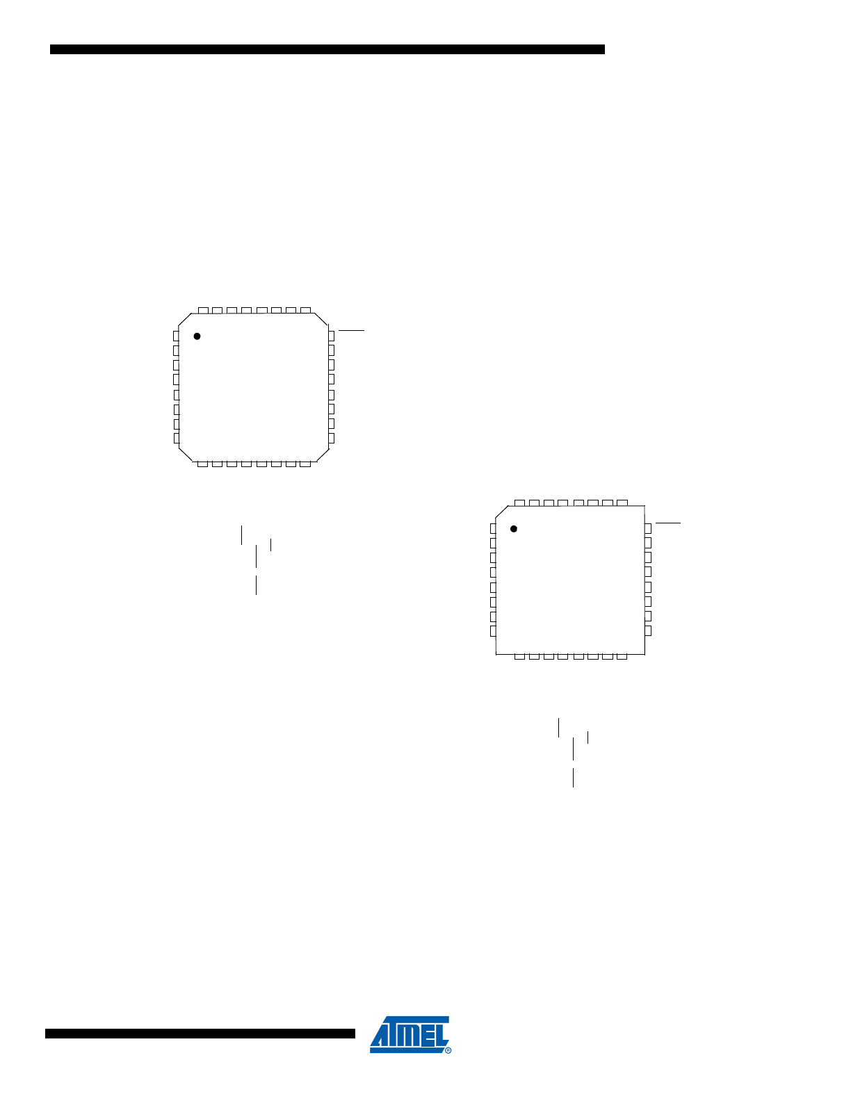
Pin Configurations
Figure 1-1.
Pinout AT90USB82/162
Note:
The large center pad underneath the QFN packages is made of metal and must be connected to
GND. It should be soldered or glued to the board to ensure good mechanical stability. If the center
pad is left unconnected, the package might loosen from the board.
.
UVCC
QFN32
(PCINT11) PC2
(OC.0B / INT0) PD0
VCC
XTAL1
(I
N
T
5)
P
D
4
(TXD1 / I
N
T3)
P
D
3
(XCK
/
P
C
INT
12)
P
D
5
PB3 (PDO / MISO / PCINT3)
GND
(PC0) XTAL2
UGND
PB4 (T1 / PCINT4)
28 27 26
1
2
3
4
5
6
7
24
23
22
21
20
19
18
12
11
10
9
13 14 15
(AIN0 / INT1) PD1
8
16
17
PB6 (PCINT6)
D- /
SD
A
T
A
D+ / S
C
K
25
29
30
31
32
PB7 (PCINT7 / OC.0A / OC.1C)
PB5 (PCINT5)
PC7 (INT4 / ICP1 / CLKO)
PC6 (OC.1A / PCINT8)
Reset (PC1 / dW)
PC5 ( PCI
N
T9
/ OC
.1
B)
PC4 (PCI
NT10)
UCAP
(RXD1 / AIN1 / INT2) PD2
(R
TS
/
INT6
) P
D
6
(CTS
/ HWB
/ T
0
/ I
N
T
7
)
P
D
7
(SS
/
PC
INT0
) P
B
0
(S
CL
K
/
PC
INT1
) P
B
1
(P
DI
/
M
O
S
I /
PC
INT2
) P
B
2
AV
C
C
UVCC
TQFP32
(PCINT11) PC2
(OC.0B / INT0) PD0
VCC
XTAL1
(I
NT5) PD4
(T
X
D
1
/
INT3
) P
D
3
(X
CK
/
P
C
INT
1
2
) P
D
5
PB3 (PDO / MISO / PCINT3)
GND
(PC0) XTAL2
UGND
PB4 (T1 / PCINT4)
28 27 26
1
2
3
4
5
6
7
24
23
22
21
20
19
18
12
11
10
9
13 14 15
(AIN0 / INT1) PD1
8
16
17
PB6 (PCINT6)
D- /
SD
A
T
A
D+ / SCK
25
29
30
31
32
PB7 (PCINT7 / OC.0A / OC.1C)
PB5 (PCINT5)
PC7 (INT4 / ICP1 / CLKO)
PC6 (OC.1A / PCINT8)
Reset (PC1 / dW)
PC5
(
PCI
N
T9
/ OC
.1
B
)
P
C
4 (
P
CINT10
)
UCA
P
(RXD1 / AIN1 / INT2) PD2
(R
TS
/
INT
6
) PD6
(CTS
/
HW
B
/ T0
/ INT7
)
P
D
7
(S
S
/
P
C
IN
T0)
PB
0
(SCL
K /
PCI
N
T1
) P
B
1
(P
DI /
M
O
S
I /
P
C
IN
T2)
PB
2
A
V
CC
4
7707FS–AVR–11/10
AT90USB82/162
2.
Overview
The AT90USB82/162 is a low-power CMOS 8-bit microcontroller based on the AVR enhanced RISC architecture. By exe-
cuting powerful instructions in a single clock cycle, the AT90USB82/162 achieves throughputs approaching 1 MIPS per
MHz allowing the system designer to optimize power consumption versus processing speed.
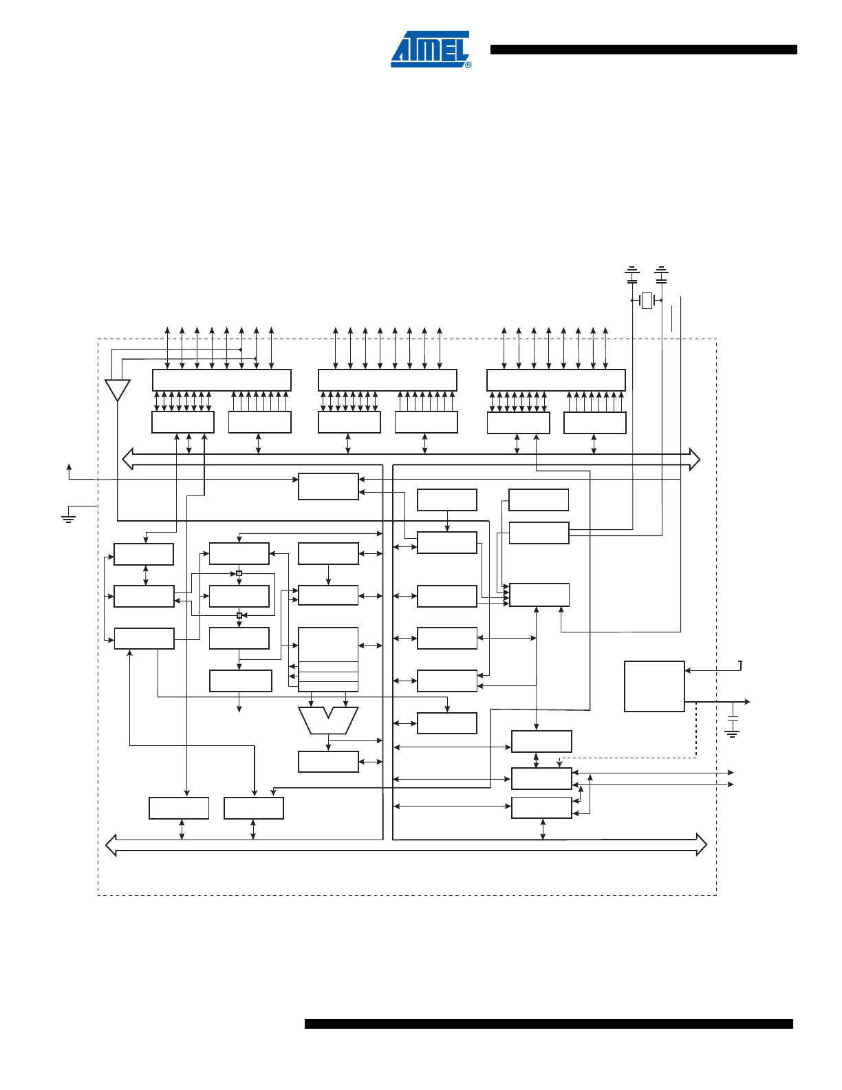
2.1
Block Diagram
Figure 2-1.
Block Diagram
The AVR core combines a rich instruction set with 32 general purpose working registers. All the
32 registers are directly connected to the Arithmetic Logic Unit (ALU), allowing two independent
registers to be accessed in one single instruction executed in one clock cycle. The resulting
PROGRAM
COUNTER
STACK
POINTER
PROGRAM
FLASH
MCU CONTROL
REGISTER
SRAM
GENERAL
PURPOSE
REGISTERS
INSTRUCTION
REGISTER
TIMER/
COUNTERS
INSTRUCTION
DECODER
DATA DIR.
REG. PORTC
DATA REGISTER
PORTC
INTERRUPT
UNIT
EEPROM
USART1
STATUS
REGISTER
Z
Y
X
ALU
PORTC DRIVERS
PORTD DRIVERS
PORTB DRIVERS
PC7 - PC0
PD7 - PD0
RESET
VCC
GND
XT
AL1
XT
AL2
CONTROL
LINES
ANALOG
COMP
ARA
T
O
R
PB7 - PB0
D+/SCK
D-/SDATA
INTERNAL
OSCILLATOR
WATCHDOG
TIMER
8-BIT DA TA BUS
USB
PS/2
TIMING AND
CONTROL
OSCILLATOR
CALIB. OSC
DATA DIR.
REG. PORTB
DATA REGISTER
PORTB
ON-CHIP DEBUG
Debug-Wire
PROGRAMMING
LOGIC
DATA DIR.
REG. PORTD
DATA REGISTER
PORTD
POR - BOD
RESET
PLL
+
-
SPI
ON-CHIP
3.3V
REGULATOR
UVcc
UCap
1uF

5
7707FS–AVR–11/10
AT90USB82/162
architecture is more code efficient while achieving throughputs up to ten times faster than con-
ventional CISC microcontrollers.
The AT90USB82/162 provides the following features: 8K / 16K bytes of In-System Programma-
ble Flash with Read-While-Write capabilities, 512 bytes EEPROM, 512 bytes SRAM, 22 general
purpose I/O lines, 32 general purpose working registers, two flexible Timer/Counters with com-
pare modes and PWM, one USART, a programmable Watchdog Timer with Internal Oscillator,
an SPI serial port, debugWIRE interface, also used for accessing the On-chip Debug system
and programming and five software selectable power saving modes. The Idle mode stops the
CPU while allowing the SRAM, Timer/Counters, SPI port, and interrupt system to continue func-
tioning. The Power-down mode saves the register contents but freezes the Oscillator, disabling
all other chip functions until the next interrupt or Hardware Reset. In Standby mode, the Crys-
tal/Resonator Oscillator is running while the rest of the device is sleeping. This allows very fast
start-up combined with low power consumption. In Extended Standby mode, the main Oscillator
continues to run.
The device is manufactured using Atmel’s high-density nonvolatile memory technology. The on-
chip ISP Flash allows the program memory to be reprogrammed in-system through an SPI serial
interface, by a conventional nonvolatile memory programmer, or by an on-chip Boot program
running on the AVR core. The boot program can use any interface to download the application
program in the application Flash memory. Software in the Boot Flash section will continue to run
while the Application Flash section is updated, providing true Read-While-Write operation. By
combining an 8-bit RISC CPU with In-System Self-Programmable Flash on a monolithic chip,
the Atmel AT90USB82/162 is a powerful microcontroller that provides a highly flexible and cost
effective solution to many embedded control applications.
The AT90USB82/162 AVR is supported with a full suite of program and system development
tools including: C compilers, macro assemblers, program debugger/simulators, in-circuit emula-
tors, and evaluation kits.
2.2
Pin Descriptions
2.2.1
VCC
Digital supply voltage.
2.2.2
GND
Ground.
2.2.3
Port B (PB7..PB0)
Port B is an 8-bit bi-directional I/O port with internal pull-up resistors (selected for each bit). The
Port B output buffers have symmetrical drive characteristics with both high sink and source
capability. As inputs, Port B pins that are externally pulled low will source current if the pull-up
resistors are activated. The Port B pins are tri-stated when a reset condition becomes active,
even if the clock is not running.
Port B also serves the functions of various special features of the AT90USB82/162 as listed on
page 74
.

6
7707FS–AVR–11/10
AT90USB82/162
2.2.4
Port C (PC7..PC0)
Port C is an 8-bit bi-directional I/O port with internal pull-up resistors (selected for each bit). The
Port C output buffers have symmetrical drive characteristics with both high sink and source
capability. As inputs, Port C pins that are externally pulled low will source current if the pull-up
resistors are activated. The Port C pins are tri-stated when a reset condition becomes active,
even if the clock is not running.
Port C also serves the functions of various special features of the AT90USB82/162 as listed on
page 76
.
2.2.5
Port D (PD7..PD0)
Port D serves as analog inputs to the analog comparator.
Port D also serves as an 8-bit bi-directional I/O port, if the analog comparator is not used (con-
cerns PD2/PD1 pins). Port pins can provide internal pull-up resistors (selected for each bit). The
Port D output buffers have symmetrical drive characteristics with both high sink and source
capability. As inputs, Port D pins that are externally pulled low will source current if the pull-up
resistors are activated. The Port D pins are tri-stated when a reset condition becomes active,
even if the clock is not running.
2.2.6
D-/SDATA
USB Full Speed Negative Data Upstream Port / Data port for PS/2
2.2.7
D+/SCK
USB Full Speed Positive Data Upstream Port / Clock port for PS/2
2.2.8
UGND
USB Ground.
2.2.9
UVCC
USB Pads Internal Regulator Input supply voltage.
2.2.10
UCAP
USB Pads Internal Regulator Output supply voltage. Should be connected to an external capac-
itor (1µF).
2.2.11
RESET/PC1/dW
Reset input. A low level on this pin for longer than the minimum pulse length will generate a
reset, even if the clock is not running. The minimum pulse length is given in
Section 9.
. Shorter
pulses are not guaranteed to generate a reset. This pin alternatively serves as debugWire chan-
nel or as generic I/O. The configuration depends on the fuses RSTDISBL and DWEN.
2.2.12
XTAL1
Input to the inverting Oscillator amplifier and input to the internal clock operating circuit.
2.2.13
XTAL2/PC0
Output from the inverting Oscillator amplifier if enabled by Fuse. Also serves as a generic I/O.

7
7707FS–AVR–11/10
AT90USB82/162
3.
About Code Examples
This documentation contains simple code examples that briefly show how to use various parts of
the device. Be aware that not all C compiler vendors include bit definitions in the header files
and interrupt handling in C is compiler dependent. Please confirm with the C compiler documen-
tation for more details.
These code examples assume that the part specific header file is included before compilation.
For I/O registers located in extended I/O map, "IN", "OUT", "SBIS", "SBIC", "CBI", and "SBI"
instructions must be replaced with instructions that allow access to extended I/O. Typically
"LDS" and "STS" combined with "SBRS", "SBRC", "SBR", and "CBR".
8
7707FS–AVR–11/10
AT90USB82/162
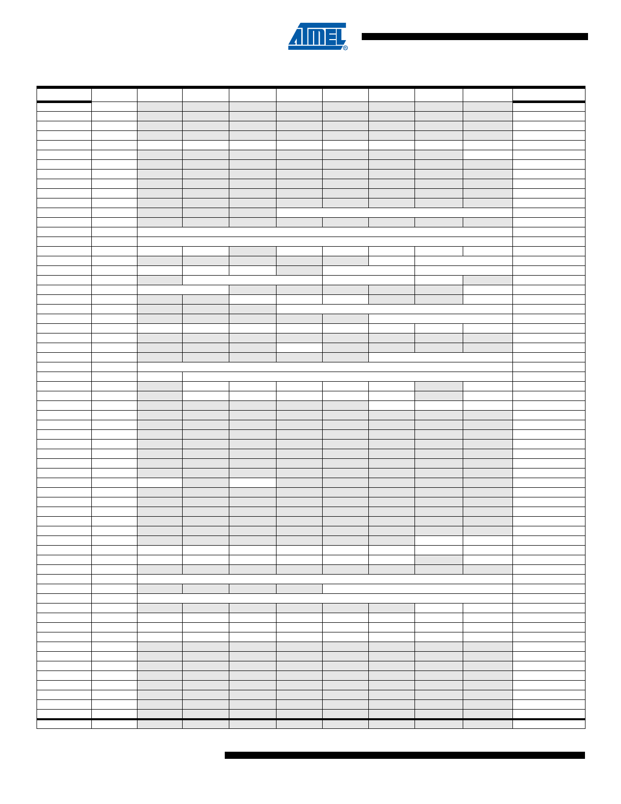
4.
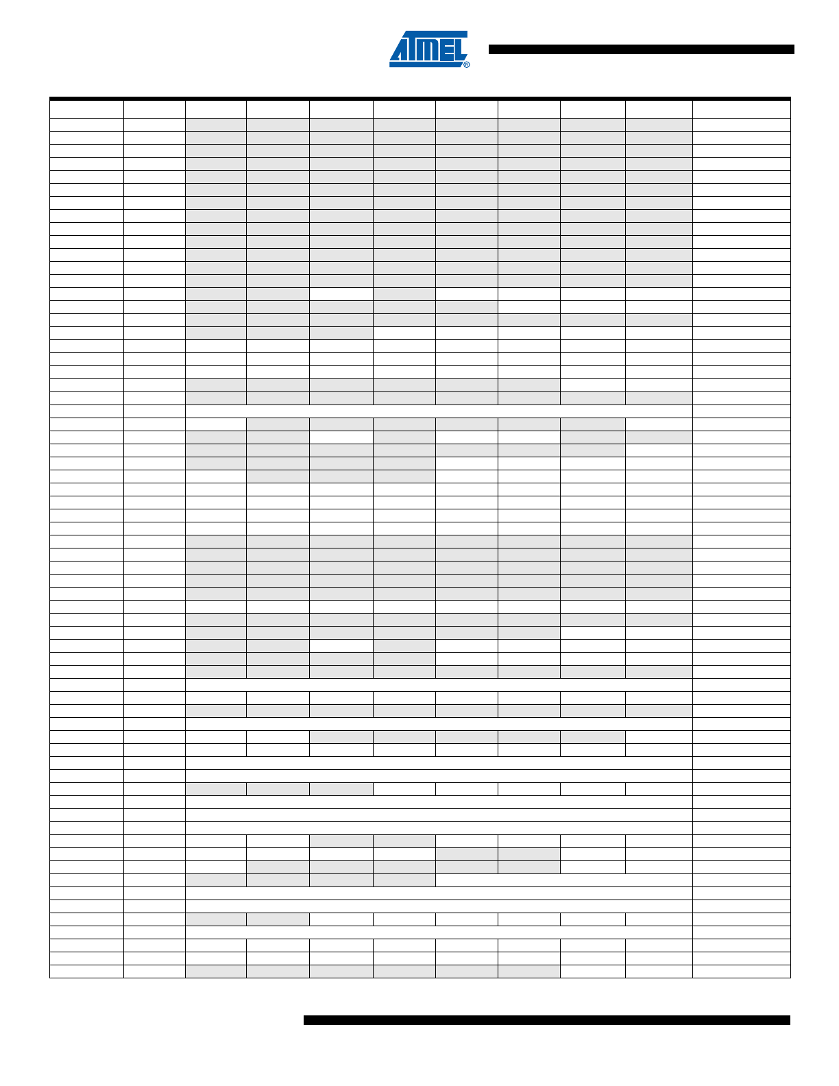
Register Summary
Address
Name
Bit 7
Bit 6
Bit 5
Bit 4
Bit 3
Bit 2
Bit 1
Bit 0
Page
(0xFF)
Reserved
-
-
-
-
-
-
-
-
(0xFE)
Reserved
-
-
-
-
-
-
-
-
(0xFD)
Reserved
-
-
-
-
-
-
-
-
(0xFC)
Reserved
-
-
-
-
-
-
-
-
(0xFB)
UPOE
UPWE1
UPWE0
UPDRV1
UPDRV0
SCKI
DATAI
DPI
DMI
(0xFA)
PS2CON
-
-
-
-
-
-
-
PS2EN
(0xF9)
Reserved
-
-
-
-
-
-
-
-
(0xF8)
Reserved
-
-
-
-
-
-
-
-
(0xF7)
Reserved
-
-
-
-
-
-
-
-
(0xF6)
Reserved
-
-
-
-
-
-
-
-
(0xF5)
Reserved
-
-
-
-
-
-
-
-
(0xF4)
UEINT
-
-
EPINT4:0
(0xF3)
Reserved
-
-
-
-
-
-
-
-
(0xF2)
UEBCLX
BYCT7:0
(0xF1)
UEDATX
DAT7:0
(0xF0)
UEIENX
FLERRE
NAKINE
-
NAKOUTE
RXSTPE
RXOUTE
STALLEDE
TXINE
(0xEF)
UESTA1X
-
-
-
-
-
CTRLDIR
CURRBK1:0
(0xEE)
UESTA0X
CFGOK
OVERFI
UNDERFI
-
DTSEQ1:0
NBUSYBK1:0
(0xED)
UECFG1X
-
EPSIZE2:0
EPBK1:0
ALLOC
-
(0xEC)
UECFG0X
EPTYPE1:0
-
-
-
-
-
EPDIR
(0xEB)
UECONX
-
-
STALLRQ
STALLRQC
RSTDT
-
-
EPEN
(0xEA)
UERST
-
-
-
EPRST4:0
(0xE9)
UENUM
-
-
-
-
-
EPNUM2:0
(0xE8)
UEINTX
FIFOCON
NAKINI
RWAL
NAKOUTI
RXSTPI
RXOUTI
STALLEDI
TXINI
(0xE7)
Reserved
-
-
-
-
-
-
-
-
(0xE6)
UDMFN
-
-
-
FNCERR
-
-
-
-
(0xE5)
UDFNUMH
-
-
-
-
-
FNUM10:8
(0xE4)
UDFNUML
FNUM7:0
(0xE3)
UDADDR
ADDEN
UADD6:0
(0xE2)
UDIEN
-
UPRSME
EORSME
WAKEUPE
EORSTE
SOFE
-
SUSPE
(0xE1)
UDINT
-
UPRSMI
EORSMI
WAKEUPI
EORSTI
SOFI
-
SUSPI
(0xE0)
UDCON
-
-
-
-
-
RSTCPU
RMWKUP
DETACH
(0xDF)
Reserved
-
-
-
-
-
-
-
-
(0xDE)
Reserved
-
-
-
-
-
-
-
-
(0xDD)
Reserved
-
-
-
-
-
-
-
-
(0xDC)
Reserved
-
-
-
-
-
-
-
-
(0xDB)
Reserved
-
-
-
-
-
-
-
-
(0xDA)
Reserved
-
-
-
-
-
-
-
-
(0xD9)
Reserved
-
-
-
-
-
-
-
-
(0xD8)
USBCON
USBE
-
FRZCLK
-
-
-
-
-
(0xD7)
Reserved
-
-
-
-
-
-
-
-
(0xD6)
Reserved
-
-
-
-
-
-
-
-
(0xD5)
Reserved
-
-
-
-
-
-
-
-
(0xD4)
Reserved
-
-
-
-
-
-
-
-
(0xD3)
Reserved
-
-
-
-
-
-
-
-
(0xD2)
CLKSTA
-
-
-
-
-
-
RCON
EXTON
(0xD1)
CLKSEL1
RCCKSEL3
RCCKSEL2
RCCKSEL1
RCCKSEL0
EXCKSEL3
EXCKSEL2
EXCKSEL1
EXCKSEL0
(0xD0)
CLKSEL0
RCSUT1
RCSUT0
EXSUT1
EXSUT0
RCE
EXTE
-
CLKS
(0xCF)
Reserved
-
-
-
-
-
-
-
-
(0xCE)
UDR1
USART1 I/O Data Register
(0xCD)
UBRR1H
-
-
-
-
USART1 Baud Rate Register High Byte
(0xCC)
UBRR1L
USART1 Baud Rate Register Low Byte
(0xCB)
UCSR1D
-
-
-
-
-
-
CTSEN
RTSEN
(0xCA)
UCSR1C
UMSEL11
UMSEL10
UPM11
UPM10
USBS1
UCSZ11
UCSZ10
UCPOL1
(0xC9)
UCSR1B
RXCIE1
TXCIE1
UDRIE1
RXEN1
TXEN1
UCSZ12
RXB81
TXB81
(0xC8)
UCSR1A
RXC1
TXC1
UDRE1
FE1
DOR1
PE1
U2X1
MPCM1
(0xC7)
Reserved
-
-
-
-
-
-
-
-
(0xC6)
Reserved
-
-
-
-
-
-
-
-
(0xC5)
Reserved
-
-
-
-
-
-
-
-
(0xC4)
Reserved
-
-
-
-
-
-
-
-
(0xC3)
Reserved
-
-
-
-
-
-
-
-
(0xC2)
Reserved
-
-
-
-
-
-
-
-
(0xC1)
Reserved
-
-
-
-
-
-
-
-
(0xC0)
Reserved
-
-
-
-
-
-
-
-
(0xBF)
Reserved
-
-
-
-
-
-
-
-
9
7707FS–AVR–11/10
AT90USB82/162
(0xBE)
Reserved
-
-
-
-
-
-
-
-
(0xBD)
Reserved
-
-
-
-
-
-
-
-
(0xBC)
Reserved
-
-
-
-
-
-
-
-
(0xBB)
Reserved
-
-
-
-
-
-
-
-
(0xBA)
Reserved
-
-
-
-
-
-
-
-
(0xB9)
Reserved
-
-
-
-
-
-
-
-
(0xB8)
Reserved
-
-
-
-
-
-
-
-
(0xB7)
Reserved
-
-
-
-
-
-
-
-
(0xB6)
Reserved
-
-
-
-
-
-
-
-
(0xB5)
Reserved
-
-
-
-
-
-
-
-
(0xB4)
Reserved
-
-
-
-
-
-
-
-
(0xB3)
Reserved
-
-
-
-
-
-
-
-
(0xB2)
Reserved
-
-
-
-
-
-
-
-
(0xB1)
Reserved
-
-
-
-
-
-
-
-
(0xB0)
Reserved
-
-
-
-
-
-
-
-
(0xAF)
Reserved
-
-
-
-
-
-
-
-
(0xAE)
Reserved
-
-
-
-
-
-
-
-
(0xAD)
Reserved
-
-
-
-
-
-
-
-
(0xAC)
Reserved
-
-
-
-
-
-
-
-
(0xAB)
Reserved
-
-
-
-
-
-
-
-
(0xAA)
Reserved
-
-
-
-
-
-
-
-
(0xA9)
Reserved
-
-
-
-
-
-
-
-
(0xA8)
Reserved
-
-
-
-
-
-
-
-
(0xA7)
Reserved
-
-
-
-
-
-
-
-
(0xA6)
Reserved
-
-
-
-
-
-
-
-
(0xA5)
Reserved
-
-
-
-
-
-
-
-
(0xA4)
Reserved
-
-
-
-
-
-
-
-
(0xA3)
Reserved
-
-
-
-
-
-
-
-
(0xA2)
Reserved
-
-
-
-
-
-
-
-
(0xA1)
Reserved
-
-
-
-
-
-
-
-
(0xA0)
Reserved
-
-
-
-
-
-
-
-
(0x9F)
Reserved
-
-
-
-
-
-
-
-
(0x9E)
Reserved
-
-
-
-
-
-
-
-
(0x9D)
Reserved
-
-
-
-
-
-
-
-
(0x9C)
Reserved
-
-
-
-
-
-
-
-
(0x9B)
Reserved
-
-
-
-
-
-
-
-
(0x9A)
Reserved
-
-
-
-
-
-
-
-
(0x99)
Reserved
-
-
-
-
-
-
-
-
(0x98)
Reserved
-
-
-
-
-
-
-
-
(0x97)
Reserved
-
-
-
-
-
-
-
-
(0x96)
Reserved
-
-
-
-
-
-
-
-
(0x95)
Reserved
-
-
-
-
-
-
-
-
(0x94)
Reserved
-
-
-
-
-
-
-
-
(0x93)
Reserved
-
-
-
-
-
-
-
-
(0x92)
Reserved
-
-
-
-
-
-
-
-
(0x91)
Reserved
-
-
-
-
-
-
-
-
(0x90)
Reserved
-
-
-
-
-
-
-
-
(0x8F)
Reserved
-
-
-
-
-
-
-
-
(0x8E)
Reserved
-
-
-
-
-
-
-
-
(0x8D)
OCR1CH
Timer/Counter1 - Output Compare Register C High Byte
(0x8C)
OCR1CL
Timer/Counter1 - Output Compare Register C Low Byte
(0x8B)
OCR1BH
Timer/Counter1 - Output Compare Register B High Byte
(0x8A)
OCR1BL
Timer/Counter1 - Output Compare Register B Low Byte
(0x89)
OCR1AH
Timer/Counter1 - Output Compare Register A High Byte
(0x88)
OCR1AL
Timer/Counter1 - Output Compare Register A Low Byte
(0x87)
ICR1H
Timer/Counter1 - Input Capture Register High Byte
(0x86)
ICR1L
Timer/Counter1 - Input Capture Register Low Byte
(0x85)
TCNT1H
Timer/Counter1 - Counter Register High Byte
(0x84)
TCNT1L
Timer/Counter1 - Counter Register Low Byte
(0x83)
Reserved
-
-
-
-
-
-
-
-
(0x82)
TCCR1C
FOC1A
FOC1B
FOC1C
-
-
-
-
-
(0x81)
TCCR1B
ICNC1
ICES1
-
WGM13
WGM12
CS12
CS11
CS10
(0x80)
TCCR1A
COM1A1
COM1A0
COM1B1
COM1B0
COM1C1
COM1C0
WGM11
WGM10
(0x7F)
Reserved
-
-
-
-
-
-
-
-
(0x7E)
Reserved
-
-
-
-
-
-
-
-
(0x7D)
Reserved
-
-
-
-
-
-
-
-
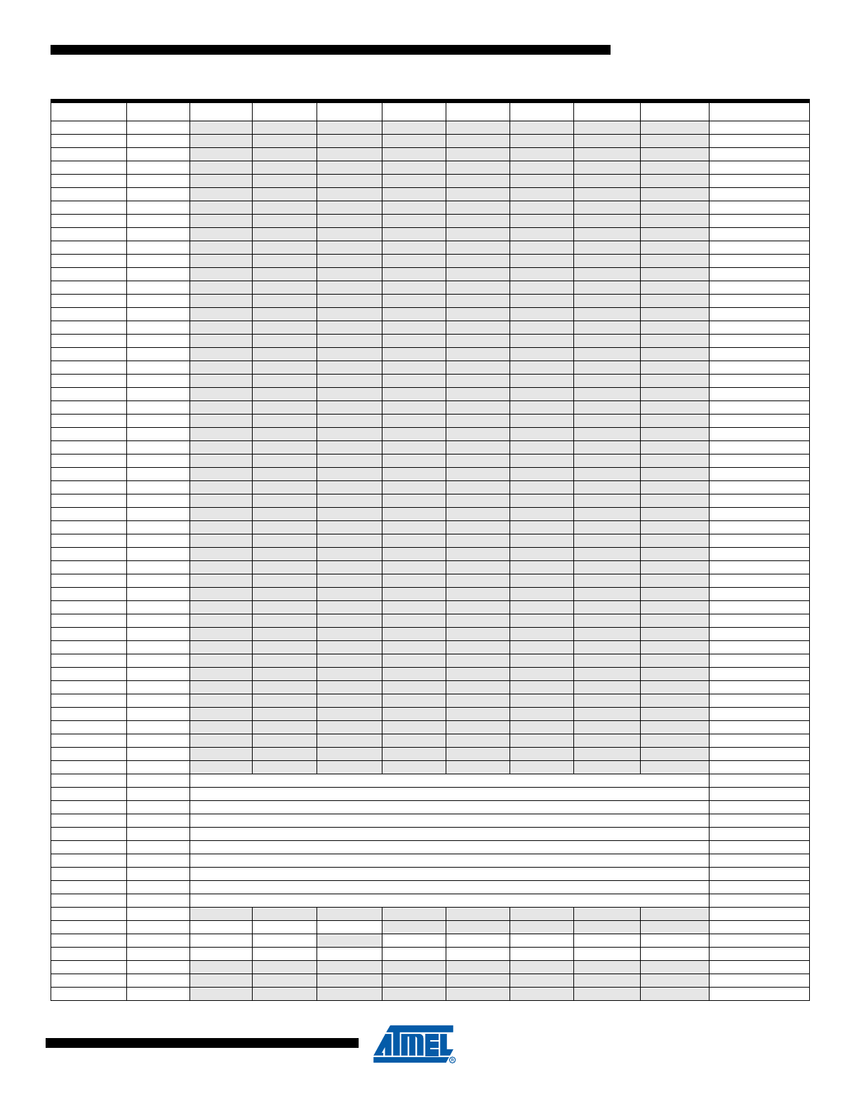
Address
Name
Bit 7
Bit 6
Bit 5
Bit 4
Bit 3
Bit 2
Bit 1
Bit 0
Page
10
7707FS–AVR–11/10
AT90USB82/162
(0x7C)
Reserved
-
-
-
-
-
-
-
-
(0x7B)
Reserved
-
-
-
-
-
-
-
-
(0x7A)
Reserved
-
-
-
-
-
-
-
-
(0x79)
Reserved
-
-
-
-
-
-
-
-
(0x78)
Reserved
-
-
-
-
-
-
-
-
(0x77)
Reserved
-
-
-
-
-
-
-
-
(0x76)
Reserved
-
-
-
-
-
-
-
-
(0x75)
Reserved
-
-
-
-
-
-
-
-
(0x74)
Reserved
-
-
-
-
-
-
-
-
(0x73)
Reserved
-
-
-
-
-
-
-
-
(0x72)
Reserved
-
-
-
-
-
-
-
-
(0x71)
Reserved
-
-
-
-
-
-
-
-
(0x70)
Reserved
-
-
-
-
-
-
-
-
(0x6F)
TIMSK1
-
-
ICIE1
-
OCIE1C
OCIE1B
OCIE1A
TOIE1
(0x6E)
TIMSK0
-
-
-
-
-
OCIE0B
OCIE0A
TOIE0
(0x6D)
Reserved
-
-
-
-
-
-
-
-
(0x6C)
PCMSK1
-
-
-
PCINT12
PCINT11
PCINT10
PCINT9
PCINT8
(0x6B)
PCMSK0
PCINT7
PCINT6
PCINT5
PCINT4
PCINT3
PCINT2
PCINT1
PCINT0
(0x6A)
EICRB
ISC71
ISC70
ISC61
ISC60
ISC51
ISC50
ISC41
ISC40
(0x69)
EICRA
ISC31
ISC30
ISC21
ISC20
ISC11
ISC10
ISC01
ISC00
(0x68)
PCICR
-
-
-
-
-
-
PCIE1
PCIE0
(0x67)
Reserved
-
-
-
-
-
-
-
-
(0x66)
OSCCAL
Oscillator Calibration Register
(0x65)
PRR1
PRUSB
-
-
-
-
-
-
PRUSART1
(0x64)
PRR0
-
-
PRTIM0
-
PRTIM1
PRSPI
-
-
(0x63)
REGCR
-
-
-
-
-
-
-
REGDIS
(0x62)
WDTCKD
-
-
-
-
WDEWIF
WDEWIE
WCLKD1
WCLKD0
(0x61)
CLKPR
CLKPCE
-
-
-
CLKPS3
CLKPS2
CLKPS1
CLKPS0
(0x60)
WDTCSR
WDIF
WDIE
WDP3
WDCE
WDE
WDP2
WDP1
WDP0
0x3F (0x5F)
SREG
I
T
H
S
V
N
Z
C
0x3E (0x5E)
SPH
SP15
SP14
SP13
SP12
SP11
SP10
SP9
SP8
0x3D (0x5D)
SPL
SP7
SP6
SP5
SP4
SP3
SP2
SP1
SP0
0x3C (0x5C)
Reserved
-
-
-
-
-
-
-
-
0x3B (0x5B)
Reserved
-
-
-
-
-
-
-
-
0x3A (0x5A)
Reserved
-
-
-
-
-
-
-
-
0x39 (0x59)
Reserved
-
-
-
-
-
-
-
-
0x38 (0x58)
Reserved
-
-
-
-
-
-
-
-
0x37 (0x57)
SPMCSR
SPMIE
RWWSB
SIGRD
RWWSRE
BLBSET
PGWRT
PGERS
SPMEN
0x36 (0x56)
Reserved
-
-
-
-
-
-
-
-
0x35 (0x55)
MCUCR
-
-
-
-
-
-
IVSEL
IVCE
0x34 (0x54)
MCUSR
-
-
USBRF
-
WDRF
BORF
EXTRF
PORF
0x33 (0x53)
SMCR
-
-
-
-
SM2
SM1
SM0
SE
0x32 (0x52)
Reserved
-
-
-
-
-
-
-
-
0x31 (0x51)
DWDR
debugWIRE Data Register
0x30 (0x50)
ACSR
ACD
ACBG
ACO
ACI
ACIE
ACIC
ACIS1
ACIS0
0x2F (0x4F)
Reserved
-
-
-
-
-
-
-
-
0x2E (0x4E)
SPDR
SPI Data Register
0x2D (0x4D)
SPSR
SPIF
WCOL
-
-
-
-
-
SPI2X
0x2C (0x4C)
SPCR
SPIE
SPE
DORD
MSTR
CPOL
CPHA
SPR1
SPR0
0x2B (0x4B)
GPIOR2
General Purpose I/O Register 2
0x2A (0x4A)
GPIOR1
General Purpose I/O Register 1
0x29 (0x49)
PLLCSR
-
-
-
PLLP2
PLLP1
PLLP0
PLLE
PLOCK
0x28 (0x48)
OCR0B
Timer/Counter0 Output Compare Register B
0x27 (0x47)
OCR0A
Timer/Counter0 Output Compare Register A
0x26 (0x46)
TCNT0
Timer/Counter0 (8 Bit)
0x25 (0x45)
TCCR0B
FOC0A
FOC0B
-
-
WGM02
CS02
CS01
CS00
0x24 (0x44)
TCCR0A
COM0A1
COM0A0
COM0B1
COM0B0
-
-
WGM01
WGM00
0x23 (0x43)
GTCCR
TSM
-
-
-
-
-
PSRASY
PSRSYNC
0x22 (0x42)
EEARH
-
-
-
-
EEPROM Address Register High Byte
0x21 (0x41)
EEARL
EEPROM Address Register Low Byte
0x20 (0x40)
EEDR
EEPROM Data Register
0x1F (0x3F)
EECR
-
-
EEPM1
EEPM0
EERIE
EEMPE
EEPE
EERE
0x1E (0x3E)
GPIOR0
General Purpose I/O Register 0
0x1D (0x3D)
EIMSK
INT7
INT6
INT5
INT4
INT3
INT2
INT1
INT0
0x1C (0x3C)
EIFR
INTF7
INTF6
INTF5
INTF4
INTF3
INTF2
INTF1
INTF0
0x1B (0x3B)
PCIFR
-
-
-
-
-
-
PCIF1
PCIF0
Address
Name
Bit 7
Bit 6
Bit 5
Bit 4
Bit 3
Bit 2
Bit 1
Bit 0
Page