

©2013 Silicon Storage Technology, Inc.
DS75056A
04/13
Data Sheet
www.microchip.com
Features
• High Gain:
– Typically 32 dB gain across 2.4–2.5 GHz over tempera-
ture 0°C to +85°C
• High linear output power:
– >29 dBm P1dB
- Please refer to “Absolute Maximum Stress Ratings” on
page 5
– Meets 802.11g OFDM ACPR requirement up to 25 dBm
– Added EVM~4% up to 23 dBm for
54 Mbps 802.11g signal
– Meets 802.11b ACPR requirement up to 25 dBm
• High power-added efficiency/Low operating cur-
rent for both 802.11g/b applications
– ~26%/300 mA @ P
OUT
= 24 dBm for 802.11g
– ~27%/350 mA @ P
OUT
= 25 dBm for 802.11b
• Built-in Ultra-low I
REF
power-up/down control
– I
REF
~2 mA
• Low idle current
– ~80 mA I
CQ
• High-speed power-up/down
– Turn on/off time (10%-90%) <100 ns
– Typical power-up/down delay with driver delay included
<200 ns
• High temperature stability
– ~1 dB gain/power variation between 0°C to +85°C
– ~1 dB detector variation over 0°C to +85°C
• Low shut-down current (~1 µA)
• On-chip power detection
• 25 dB dynamic range on-chip power detection
• Simple input/output matching
• Packages available
– 16-contact VQFN (3mm x 3mm)
• All non-Pb (lead-free) devices are RoHS compliant
Applications
• WLAN (IEEE 802.11b/g/n)
• Home RF
• Cordless phones
• 2.4 GHz ISM wireless equipment
2.4 GHz High-Power and High-Gain Power Amplifier
SST12LP15A
The SST12LP15A is a high-power and high-gain power amplifier based on the
highly-reliable InGaP/GaAs HBT technology. Easily configured for high-power
applications with superb power-added efficiency while operating over the 2.4-2.5
GHz frequency band, it typically provides 32 dB gain with 26% power-added effi-
ciency @ P
OUT
= 24 dBm for 802.11g and 27% power-added efficiency @ P
OUT
=
25 dBm for 802.11b. The SST12LP15A has excellent linearity while meeting
802.11g spectrum mask at 25 dBm. The power amplifier IC features easy board-
level usage along with high-speed power-up/down control and is offered in 16-
contact VQFN package

©2013 Silicon Storage Technology, Inc.
DS75056A
04/13
2
2.4 GHz High-Power and High-Gain Power Amplifier
SST12LP15A
Data Sheet
Product Description
The SST12LP15A is a high-power and high-gain power amplifier based on the highly-reliable InGaP/
GaAs HBT technology.
The SST12LP15A can be easily configured for high-power applications with superb power-added effi-
ciency while operating over the 2.4-2.5 GHz frequency band. It typically provides 32 dB gain with 26%
power-added efficiency @ P
OUT
= 24 dBm for 802.11g and 27% power-added efficiency @ P
OUT
= 25
dBm for 802.11b.
The SST12LP15A has excellent linearity, typically ~4% added EVM at 23 dBm output power which is
essential for 54 Mbps 802.11g operation while meeting 802.11g spectrum mask at 25 dBm.
SST12LP15A also has wide-range (>25 dB), temperature-stable (~1 dB over 85°C), single-ended/dif-
ferential power detectors which lower users’ cost on power control.
The power amplifier IC also features easy board-level usage along with high-speed power-up/down
control. Ultra-low reference current (total I
REF
~2 mA) makes the SST12LP15A controllable by an on/
off switching signal directly from the baseband chip. These features coupled with low operating current
make the SST12LP15A ideal for the final stage power amplification in battery-powered 802.11b/g/n
WLAN transmitter applications.
The SST12LP15A is offered in 16-contact VQFN package. See Figure 2 for pin assignments and Table
1 for pin descriptions.
©2013 Silicon Storage Technology, Inc.
DS75056A
04/13
3
2.4 GHz High-Power and High-Gain Power Amplifier
SST12LP15A
Data Sheet
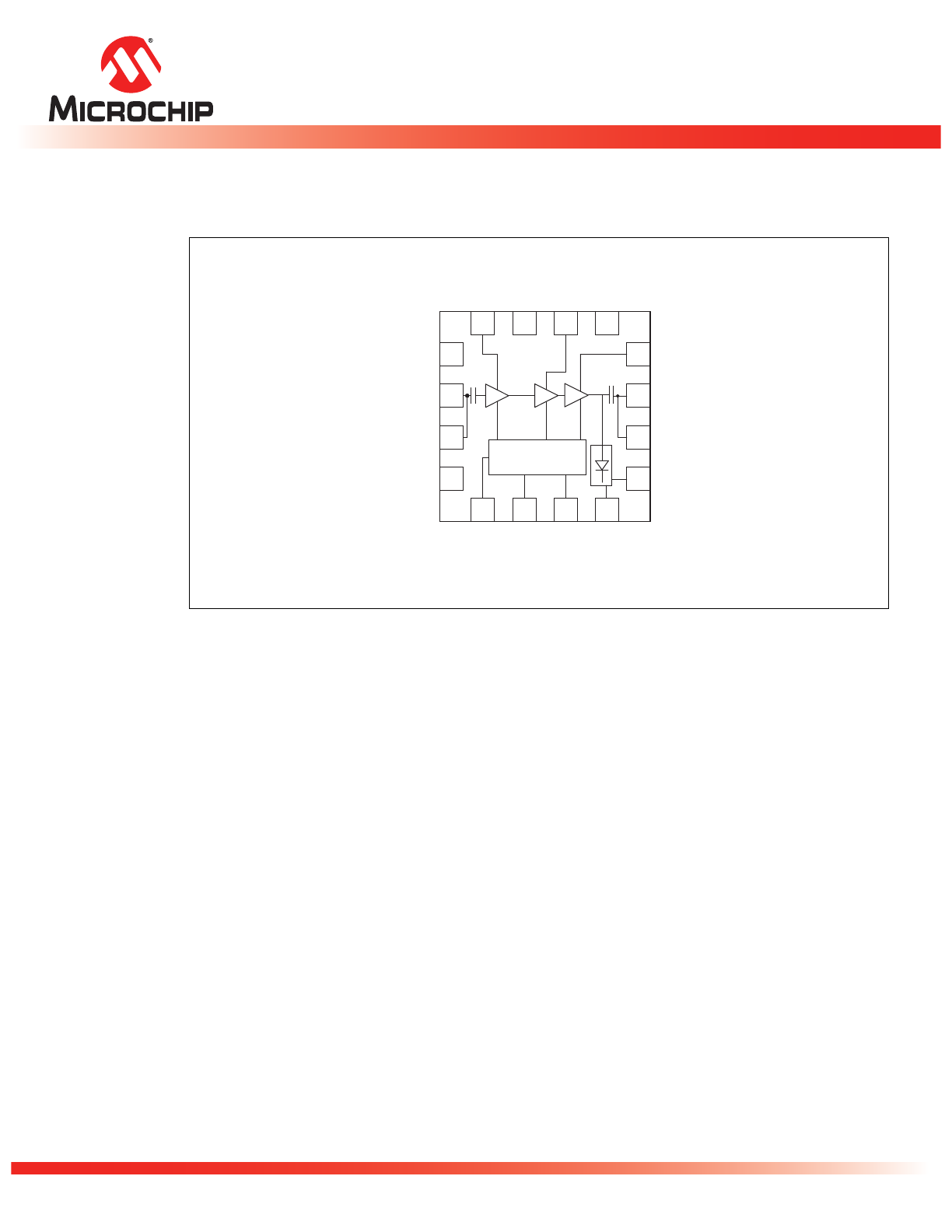
Functional Blocks
Figure 1: Functional Block Diagram6
2
5
6
8
16
VCC1
15
1
14
VCC2
NC
4
9
11
12
10
13
NC
VCCb
VREF1
VREF2
Det_ref
VCC3
RFOUT
RFOUT
Det
NC
3
RFIN
RFIN
NC
Bias Circuit
7
1291 B1.0
©2013 Silicon Storage Technology, Inc.
DS75056A
04/13
4
2.4 GHz High-Power and High-Gain Power Amplifier
SST12LP15A
Data Sheet
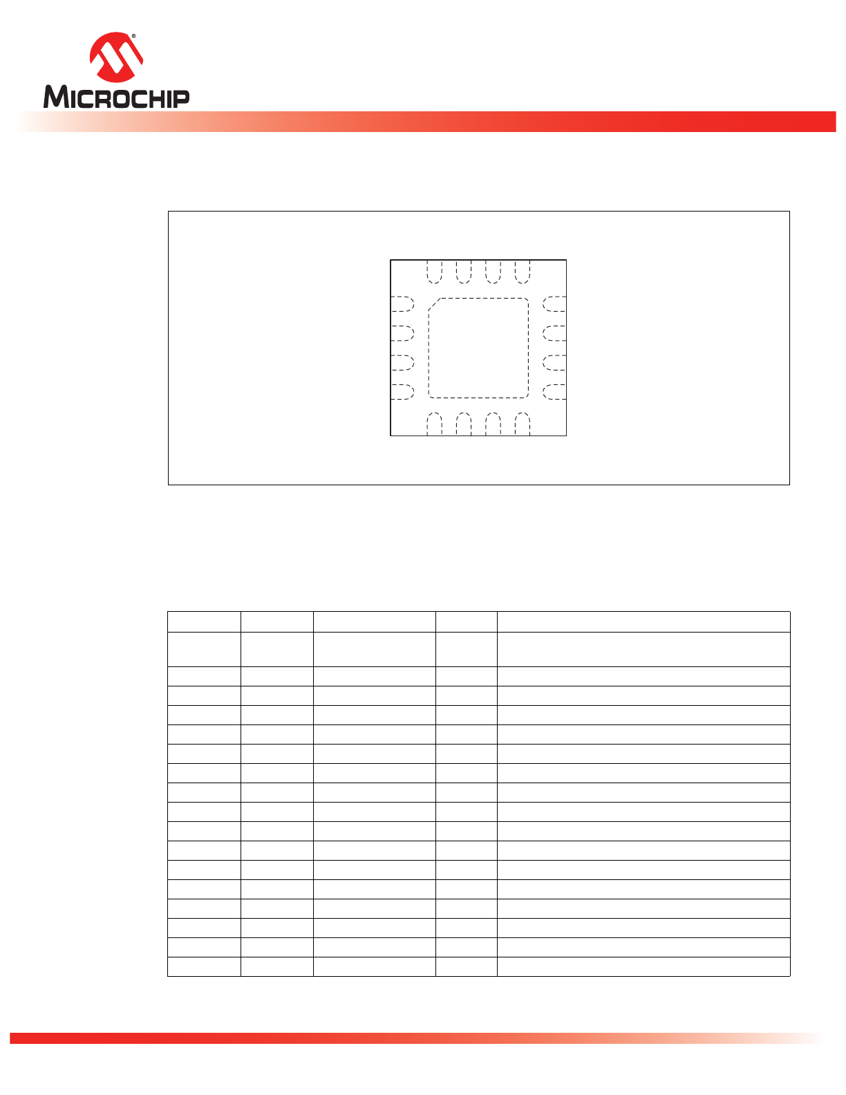
Pin Assignments
Figure 2: Pin Assignments for 16-contact VQFN
Pin Descriptions
Table 1: Pin Description
Symbol
Pin No.
Pin Name
Type
1
1. I=Input, O=Output
Function
GND
0
Ground
The center pad should be connected to RF ground
with several low inductance, low resistance vias.
NC
1
No Connection
Unconnected pins.
RFIN
2
I
RF input, DC decoupled
RFIN
3
I
RF input, DC decoupled
NC
4
No Connection
Unconnected pins.
VCCb
5
Power Supply
PWR
Supply voltage for bias circuit
VREF1
6
PWR
1st and 2nd stage idle current control
VREF2
7
PWR
3rd stage idle current control
Det_ref
8
O
On-chip power detector reference
Det
9
O
On-chip power detector
RFOUT
10
O
RF output
RFOUT
11
O
RF output
VCC3
12
Power Supply
PWR
Power supply, 3rd stage
NC
13
No Connection
Unconnected pins.
VCC2
14
Power Supply
PWR
Power supply, 2nd stage
NC
15
No Connection
Unconnected pins.
VCC1
16
Power Supply
PWR
Power supply, 1st stage
T1.0 75056
5
6
8
16
VCC1
15
14
VCC2
NC
9
11
12
10
13
NC
VCCb
VREF1
VREF2
Det_ref
VCC3
RFOUT
RFOUT
Det
2
1
4
3
NC
RFIN
RFIN
NC
7
1291 16-vqfn P1.0
Top View
(contacts facing down)
RF and DC GND
0
©2013 Silicon Storage Technology, Inc.
DS75056A
04/13
5
2.4 GHz High-Power and High-Gain Power Amplifier
SST12LP15A
Data Sheet
Electrical Specifications
The AC and DC specifications for the power amplifier interface signals. Refer to Table 3 for the DC volt-
age and current specifications. Refer to Figures 3 through 10 for the RF performance.
Absolute Maximum Stress Ratings (Applied conditions greater than those listed under “Absolute
Maximum Stress Ratings” may cause permanent damage to the device. This is a stress rating only and
functional operation of the device at these conditions or conditions greater than those defined in the
operational sections of this data sheet is not implied. Exposure to absolute maximum stress rating con-
ditions may affect device reliability.)
Input power to pins 2 and 3 (P
IN
) . . . . . . . . . . . . . . . . . . . . . . . . . . . . . . . . . . . . . . . . . . . . . . . +5 dBm
Average output power (P
OUT
)
1
. . . . . . . . . . . . . . . . . . . . . . . . . . . . . . . . . . . . . . . . . . . . . . . . +28 dBm
1. Never measure with CW source. Pulsed single-tone source with <50% duty cycle is recommended. Exceeding the max-
imum rating of average output power could cause permanent damage to the device.
Supply Voltage at pins 5, 12, 14, 16 (V
CC
). . . . . . . . . . . . . . . . . . . . . . . . . . . . . . . . . . . -0.3V to +4.6V
Reference voltage to pins 6 (V
REF1
) and pin 7 (V
REF2
) . . . . . . . . . . . . . . . . . . . . . . . . . -0.3V to +3.6V
DC supply current (I
CC
) . . . . . . . . . . . . . . . . . . . . . . . . . . . . . . . . . . . . . . . . . . . . . . . . . . . . . . 500 mA
Operating Temperature (T
A
) . . . . . . . . . . . . . . . . . . . . . . . . . . . . . . . . . . . . . . . . . . . . . -40ºC to +85ºC
Storage Temperature (T
STG
) . . . . . . . . . . . . . . . . . . . . . . . . . . . . . . . . . . . . . . . . . . . -40ºC to +120ºC
Maximum Junction Temperature (T
J
) . . . . . . . . . . . . . . . . . . . . . . . . . . . . . . . . . . . . . . . . . . . . .+150ºC
Surface Mount Solder Reflow Temperature . . . . . . . . . . . . . . . . . . . . . . . . . . . . 260°C for 10 seconds
Table 2: Operating Range
Range
Ambient Temp
V
DD
Industrial
-40°C to +85°C
3.3V
T2.1 75056
Table 3: DC Electrical Characteristics at 25ºC
Symbol
Parameter
Min.
Typ
Max.
Unit
V
CC
Supply Voltage at pins 5, 12, 14, 16
3.0
3.3
4.2
V
I
CC
Supply Current
for 802.11g, 24 dBm
300
mA
for 802.11b, 25 dBm
350
mA
I
CQ
Idle current for 802.11g to meet EVM<4% @ 23dBm
80
mA
I
OFF
Shut down current
1
µA
V
REG1
Reference Voltage for 1st and 2nd Stage, with 270
Ω
resistor
2.85
2.90
2.95
V
V
REG2
Reference Voltage for 3rd Stage, with 100
Ω
resistor
2.85
2.90
2.95
V
T3.1 75056
©2013 Silicon Storage Technology, Inc.
DS75056A
04/13
6
2.4 GHz High-Power and High-Gain Power Amplifier
SST12LP15A
Data Sheet
Table 4: AC Electrical Characteristics for Configuration at 25ºC
Symbol
Parameter
Min.
Typ
Max.
Unit
F
L-U
Frequency range in 802.11b/g applications (see Fig-
ure 11)
2400
2485
MHz
P
OUT
Output power
@ PIN = -10 dBm 11b signals
23
dBm
@ PIN = -10 dBm 11g signals
23
dBm
G
Small signal gain
31
32
dB
G
VAR1
Gain variation over each band (2400-2485 MHz)
±0.5
dB
G
VAR2
Gain ripple over channel (Gain variation over 20
MHz)
0.2
dB
ACPR
Meet 11b spectrum mask
24
25
dBm
Meet 11g OFDM 54 MBPS spectrum mask
24
25
dBm
Added EVM @ 23 dBm output with 11g OFDM 54 MBPS signal
3.5
%
2f, 3f, 4f, 5f
Harmonics at 22 dBm, without trapping capacitors
-40
dBc
T4.2 75056
©2013 Silicon Storage Technology, Inc.
DS75056A
04/13
7
2.4 GHz High-Power and High-Gain Power Amplifier
SST12LP15A
Data Sheet
Typical Performance Characteristics
Test Conditions: V
CC
= 3.3V, T
A
= 25°C Unless otherwise specified.
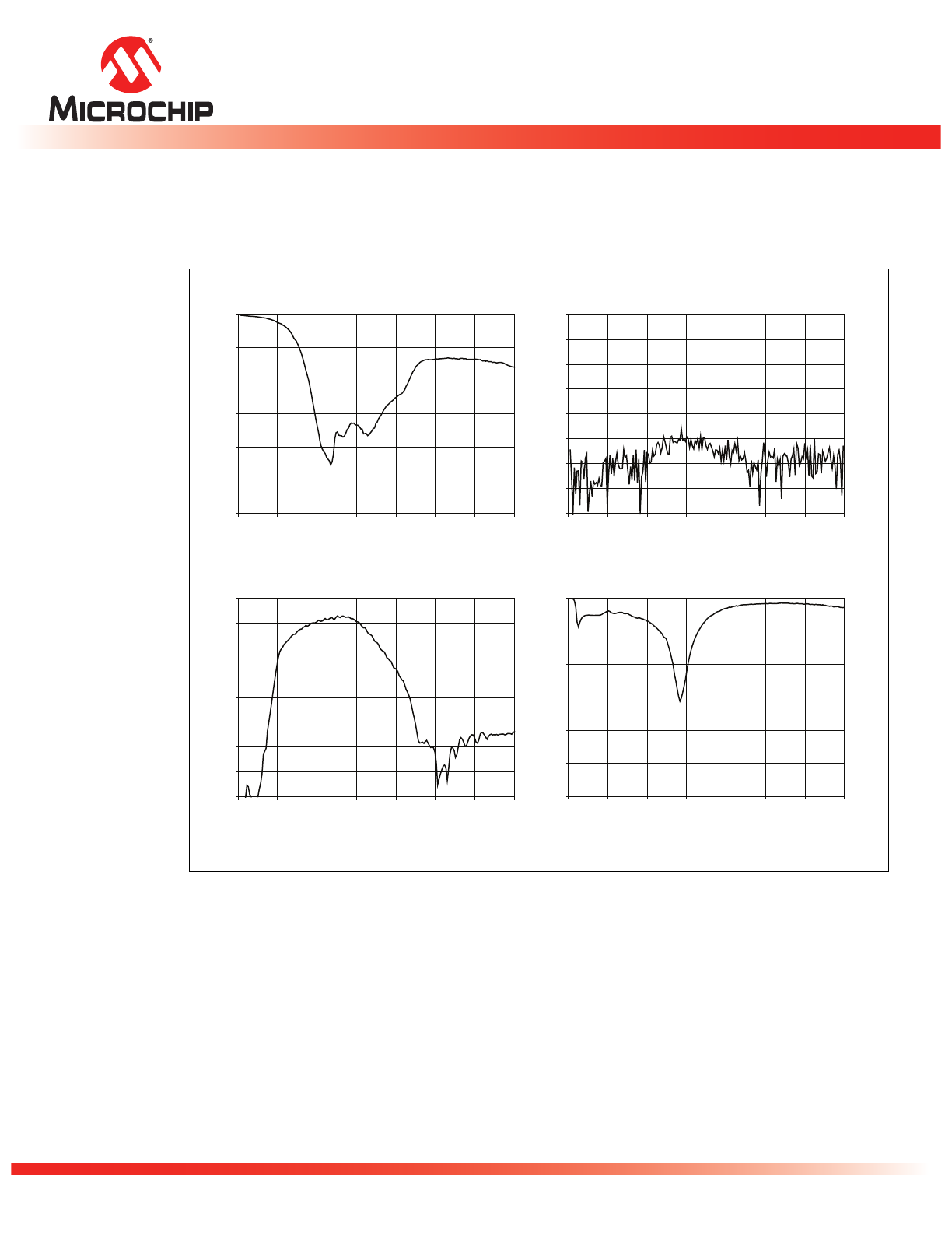
Figure 3: S-Parameters
1291 S-Parms.0.1
-30
-25
-20
-15
-10
-5
0
0.0
1.0
2.0
3.0
4.0
5.0
6.0
7.0
Frequency (GHz)
S11 (dB)
S12 versus Frequency
-80
-70
-60
-50
-40
-30
-20
-10
0
0.0
1.0
2.0
3.0
4.0
5.0
6.0
7.0
Frequency (GHz)
S12 (dB)
S11 versus Frequency
S21 versus Frequency
-40
-30
-20
-10
0
10
20
30
40
0.0
1.0
2.0
3.0
4.0
5.0
6.0
7.0
Frequency (GHz)
S21 (dB)
S22 versus Frequency
-30
-25
-20
-15
-10
-5
0
0.0
1.0
2.0
3.0
4.0
5.0
6.0
7.0
Frequency (GHz)
S22 (dB)
©2013 Silicon Storage Technology, Inc.
DS75056A
04/13
8
2.4 GHz High-Power and High-Gain Power Amplifier
SST12LP15A
Data Sheet
Typical Performance Characteristics
Test Conditions: V
CC
= 3.3V, T
A
= 25°C, 54 Mbps 802.11g OFDM Signal
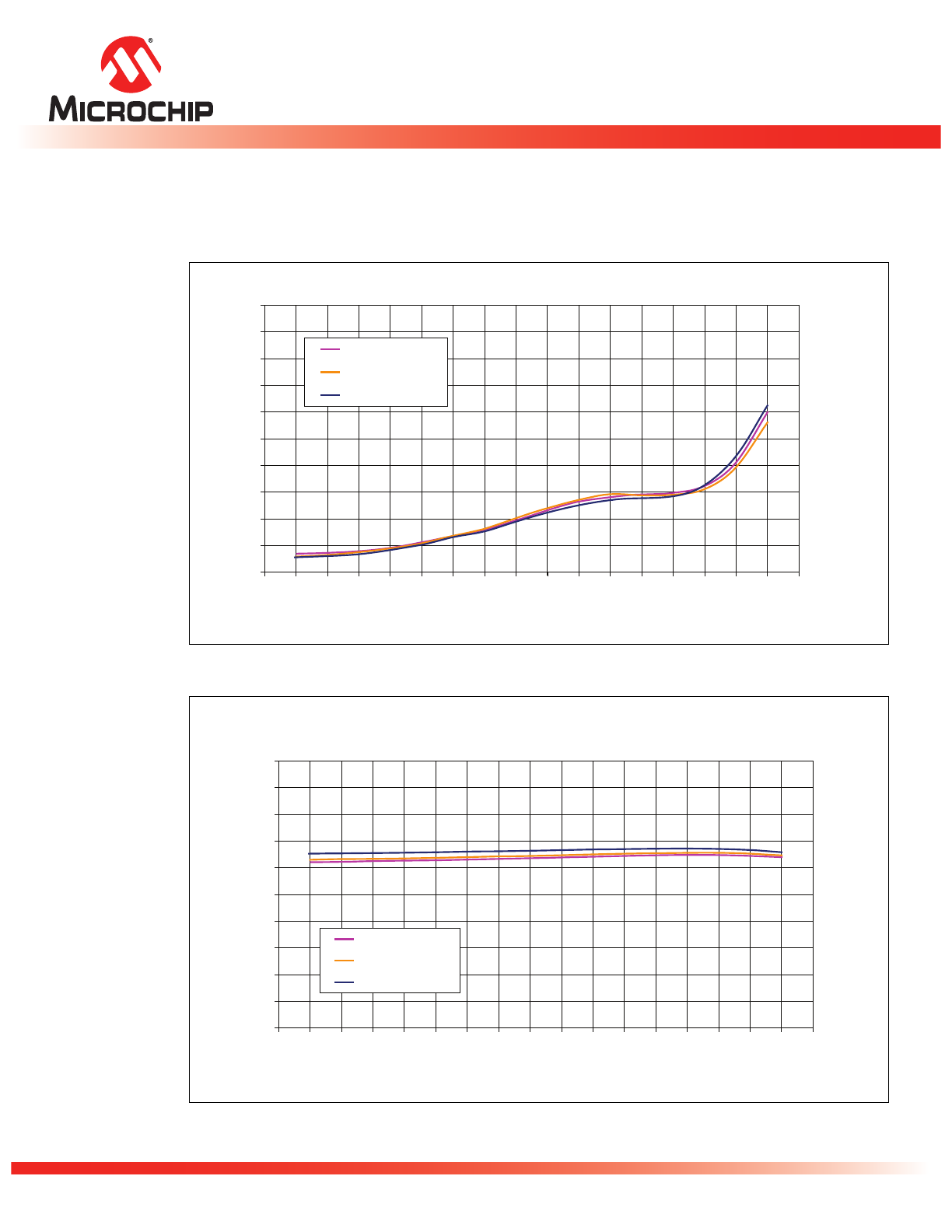
Figure 4: EVM versus Output Power measured with “Data plus Sequence” channel estimation
Figure 5: Power Gain versus Output Power
EVM versus Output Power
0
1
2
3
4
5
6
7
8
9
10
9
10
11
12
13
14
15
16
17
18
19
20
21
22
23
24
25
26
Output Power (dBm)
EVM (%)
Freq=2.412 GHz
Freq=2.442 GHz
Freq=2.484 GHz
1291 F4.0
1291 F5.0
Power Gain versus Output Power
20
22
24
26
28
30
32
34
36
38
40
9
10
11
12
13
14
15
16
17
18
19
20
21
22
23
24
25
26
Output Power (dBm)
P
o
wer Gain (dB)
Freq=2.412 GHz
Freq=2.442 GHz
Freq=2.484 GHz
©2013 Silicon Storage Technology, Inc.
DS75056A
04/13
9
2.4 GHz High-Power and High-Gain Power Amplifier
SST12LP15A
Data Sheet
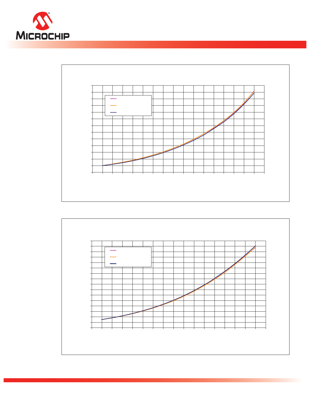
Figure 6: Total Current Consumption for 802.11g Operation versus Output Power
Figure 7: PAE versus Output Power
1291 F6.0
Supply Current versus Output Power
80
100
120
140
160
180
200
220
240
260
280
300
320
340
9
10
11
12
13
14
15
16
17
18
19
20
21
22
23
24
25
26
Output Power (dBm)
Supply Current (mA)
Freq=2.412 GHz
Freq=2.442 GHz
Freq=2.484 GHz
1291 F7.0
PAE versus Output Power
0
2
4
6
8
10
12
14
16
18
20
22
24
26
28
30
32
9
10
11
12
13
14
15
16
17
18
19
20
21
22
23
24
25
26
Output Power (dBm)
PAE (%)
Freq=2.412 GHz
Freq=2.442 GHz
Freq=2.484 GHz
©2013 Silicon Storage Technology, Inc.
DS75056A
04/13
10
2.4 GHz High-Power and High-Gain Power Amplifier
SST12LP15A
Data Sheet
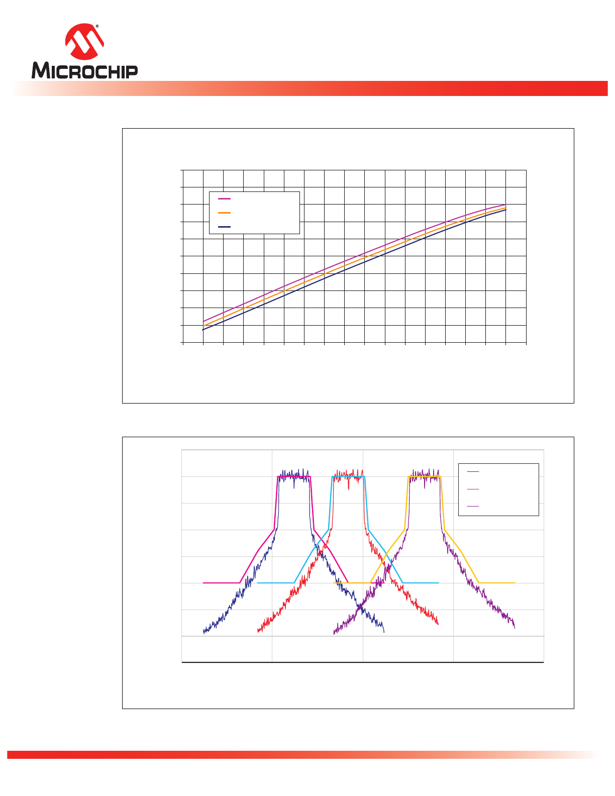
Figure 8: Detector Characteristic versus Output Power
Figure 9: 802.11g Spectrum Mask at 24 dBm, Total current 300 mA
1291 F8.0
Detector Voltage versus Output Power
1.0
1.1
1.2
1.3
1.4
1.5
1.6
1.7
1.8
1.9
2.0
9
10
11
12
13
14
15
16
17
18
19
20
21
22
23
24
25
26
Output Power (dBm)
Detector V
olta
g
e (V)
Freq=2.412 GHz
Freq=2.442 GHz
Freq=2.484 GHz
-7 0
-6 0
-5 0
-4 0
-3 0
-2 0
-1 0
0
10
2.35
2.40
2.45
2.50
2.55
Frequency (GHz)
1291 F09.0
Amplitude (dB)
Freq = 2.412 GHz
Freq = 2.442 GHz
Freq = 2.484 GHz