

Microchip Proprietary Information
©2013 Silicon Storage Technology, Inc.
DS75054A
01/13
Data Sheet
www.microchip.com
Features
• High Gain:
– Typically 33 dB gain across 2.4–2.5 GHz over tempera-
ture -40°C to +85°C
• High linear output power:
– >30 dBm P1dB
- Please refer to “Absolute Maximum Stress Ratings” on
page 5
– Meets 802.11g OFDM spectrum mask requirement up
to 28.5 dBm
– EVM~3% up to 25 dBm for 54 Mbps 802.11g signal
– 2.5% EVM up to 23.5 dBm, 802.11n, HT40
– 1.75% EVM up to 21.5 dBm, 802.11ac MCS8
– Meets 802.11b ACPR requirement up to 28.5 dBm
• High-speed power-up/down
– Turn on/off time (10%-90%) <100 ns
• 10:1 VSWR survivability (unconditionally stable up
to 28.5 dBm)
• On-chip power detection
– 20 dB dynamic range
– VSWR- and temperature-insensitive
• Simple input/output matching
• Packages available
– 16-contact VQFN (3mm x 3mm)
• All non-Pb (lead-free) devices are RoHS compliant
Applications
• WLAN (IEEE 802.11b/g/n)
• AP router
• WiMax (IEEE 802.16e)
• Home RF
• Cordless phones
• 2.4 GHz ISM wireless equipment
• 1.8 GHz Pico Cell
2.4 GHz High-Power and High-Gain Power Amplifier
SST12CP11
SST12CP11 is a high-power and high-gain power amplifier (PA) based on the
highly-reliable InGaP/GaAs HBT technology.This PA can be easily configured for
high-power applications with good power-added efficiency while operating over the
2.4-2.5 GHz frequency band. It can also be configured to operate at 1.8 GHz for
Pico Cell applications. SST12CP11 typically provides 33 dB gain and has excellent
linearity, typically ~3% EVM at 25 dBm output power at 54 Mbps 802.11g operation
while meeting 802.11g spectrum mask at 28.5 dBm. The power amplifier IC
includes an output power detector that has a wide dynamic range and is VSWR-
insensitive. SST12CP11 features easy board-level usage along with high-speed
power-up/-down control and is offered in 16-contact VQFN package.

Microchip Proprietary Information
©2013 Silicon Storage Technology, Inc.
DS75054A
01/13
2
2.4 GHz High-Power and High-Gain Power Amplifier
SST12CP11
Data Sheet
Product Description
SST12CP11 is a high-power and high-gain power amplifier (PA) based on the highly-reliable InGaP/
GaAs HBT technology.
This PA can be easily configured for high-power applications with high power-added efficiency while
operating over the 2.4-2.5 GHz frequency band. It typically provides 33 dB gain with 15% power-added
efficiency @ P
OUT
= 25 dBm for 802.11g.
SST12CP11 has excellent linearity, typically 3% added EVM at 25 dBm output power with 54 Mbps
802.11g operation while meeting 802.11g spectrum mask at 28.5 dBm. SST12CP11 also has a single-
ended power detector which lowers the users’ cost for power control.
The power amplifier IC also features easy board-level usage along with high-speed power-up/-down
control.
SST12CP11 is offered in 16-contact VQFN package. See Figure 2 for pin assignments and Table 1 for
pin descriptions.
Microchip Proprietary Information
©2013 Silicon Storage Technology, Inc.
DS75054A
01/13
3
2.4 GHz High-Power and High-Gain Power Amplifier
SST12CP11
Data Sheet
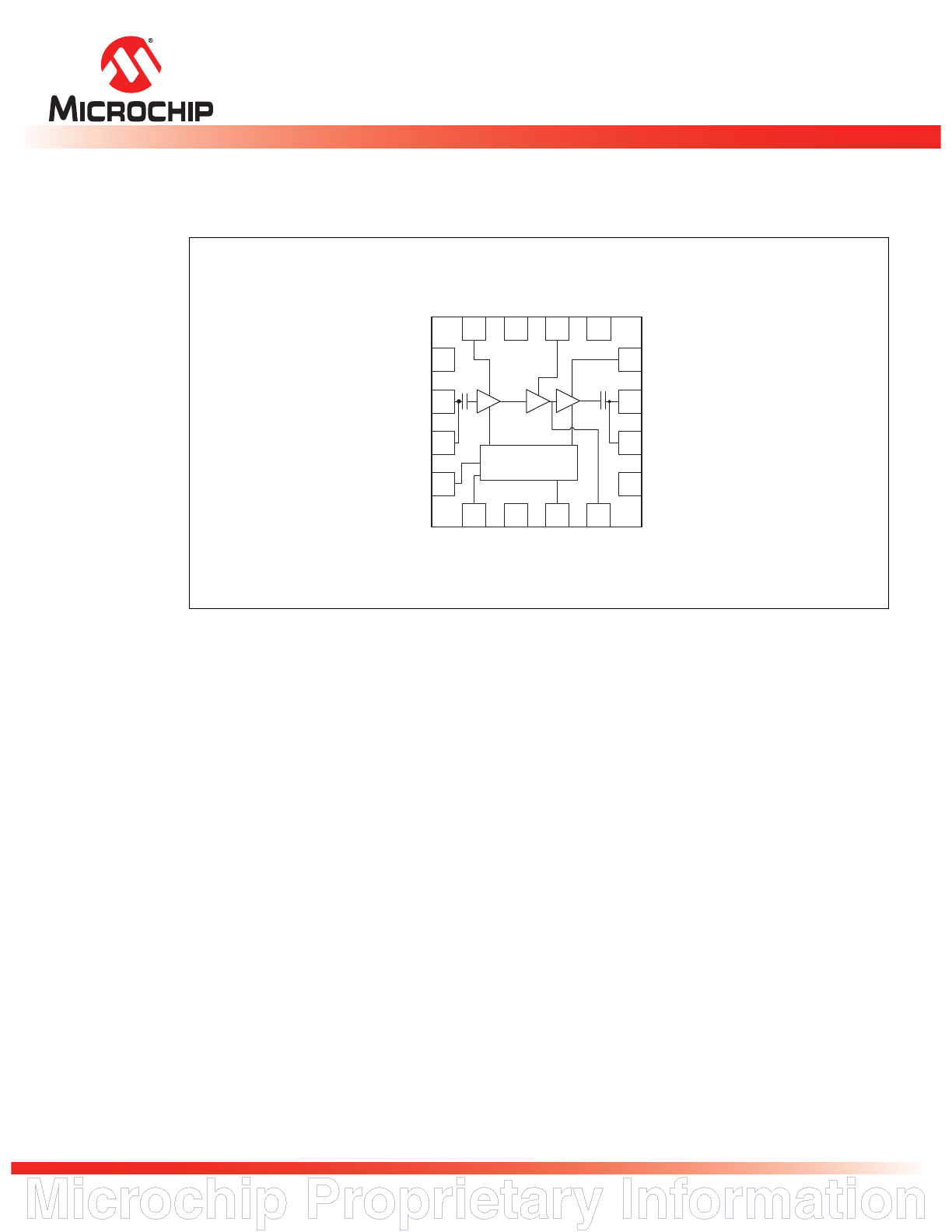
Functional Blocks
Figure 1: Functional Block Diagram
2
5
6
8
16
VCC1
15
1
14
VCC2
NC
4
9
11
12
10
13
NC
VCCb
GND
VREF2
DET
VCC3
RFOUT
RFOUT
NC
NC
3
RFIN
RFIN
VREF1
Bias Circuit
7
1403 B1.1
Microchip Proprietary Information
©2013 Silicon Storage Technology, Inc.
DS75054A
01/13
4
2.4 GHz High-Power and High-Gain Power Amplifier
SST12CP11
Data Sheet
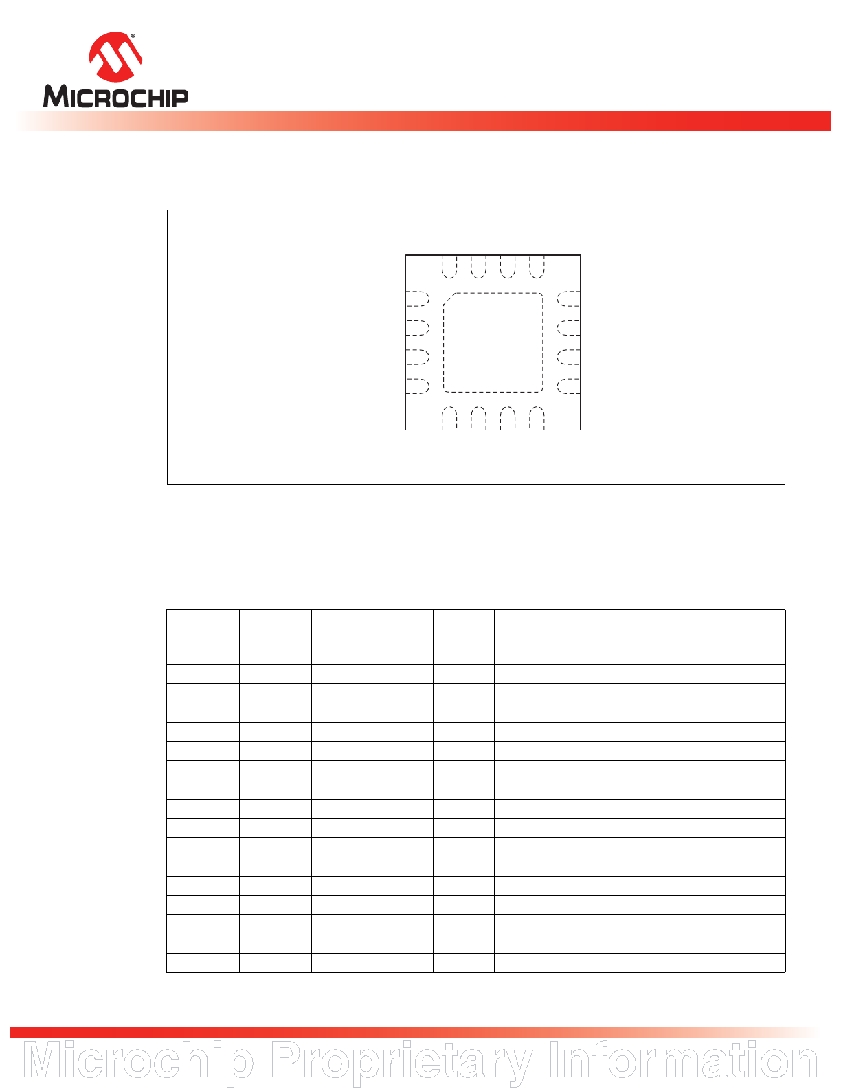
Pin Assignments
Figure 2: Pin Assignments for 16-contact VQFN
Pin Descriptions
Table 1: Pin Description
Symbol
Pin No.
Pin Name
Type
1
1. I=Input, O=Output
Function
GND
0
Ground
The center pad should be connected to RF ground
with several low inductance, low resistance vias.
NC
1
No Connection
Unconnected pins.
RFIN
2
I
RF input, DC decoupled
RFIN
3
I
RF input, DC decoupled
VREF1
4
Power Supply
PWR
1
st
stage, idle-current control
VCCb
5
Power Supply
PWR
Supply voltage for bias circuit
GND
6
Ground
VREF2
7
Power supply
PWR
2
nd
and 3
rd
stage, idle-current control
Det
8
O
On-chip power detector
NC
9
No Connection
Unconnected pins.
RFOUT
10
O
RF output
RFOUT
11
O
RF output
VCC3
12
Power Supply
PWR
Power supply, 3rd stage
NC
13
No Connection
Unconnected pins.
VCC2
14
Power Supply
PWR
Power supply, 2nd stage
NC
15
No Connection
Unconnected pins.
VCC1
16
Power Supply
PWR
Power supply, 1st stage
T1.0 75054
5
6
8
16
VCC1
15
14
VCC2
NC
9
11
12
10
13
NC
VCCb
GND
VREF2
DET
VCC3
RFOUT
RFOUT
NC
2
1
4
3
NC
RFIN
RFIN
VREF1
7
1403 16-vqfn P1.0
Top View
(contacts facing down)
RF and DC GND
0
Microchip Proprietary Information
©2013 Silicon Storage Technology, Inc.
DS75054A
01/13
5
2.4 GHz High-Power and High-Gain Power Amplifier
SST12CP11
Data Sheet
Electrical Specifications
The AC and DC specifications for the power amplifier interface signals. Refer to Table 3 for the DC volt-
age and current specifications. Refer to Figures 3 through 21 for the RF performance.
Absolute Maximum Stress Ratings (Applied conditions greater than those listed under “Absolute
Maximum Stress Ratings” may cause permanent damage to the device. This is a stress rating only and
functional operation of the device at these conditions or conditions greater than those defined in the
operational sections of this data sheet is not implied. Exposure to absolute maximum stress rating con-
ditions may affect device reliability.)
Input power to pins 2 and 3 (P
IN
) . . . . . . . . . . . . . . . . . . . . . . . . . . . . . . . . . . . . . . . . . . . . . . . . -3 dBm
Supply Voltage at pins 5, 12, 14, 16 (V
CC
). . . . . . . . . . . . . . . . . . . . . . . . . . . . . . . . . . . . . . . . . . +5.5V
Reference voltage to pins 4 (V
REF1
) and pin 7 (V
REF2
) . . . . . . . . . . . . . . . . . . . . . . . . . . . . . . . . +3.1V
DC supply current (I
CC
) . . . . . . . . . . . . . . . . . . . . . . . . . . . . . . . . . . . . . . . . . . . . . . . . . . . . . . 650 mA
Operating Temperature (T
A
) . . . . . . . . . . . . . . . . . . . . . . . . . . . . . . . . . . . . . . . . . . . . . -40ºC to +85ºC
Storage Temperature (T
STG
) . . . . . . . . . . . . . . . . . . . . . . . . . . . . . . . . . . . . . . . . . . . -40ºC to +120ºC
Maximum Junction Temperature (T
J
) . . . . . . . . . . . . . . . . . . . . . . . . . . . . . . . . . . . . . . . . . . . . .+150ºC
Surface Mount Solder Reflow Temperature . . . . . . . . . . . . . . . . . . . . . . . . . . . . 260°C for 10 seconds
Table 2: Operating Range
Range
Ambient Temp
V
CC
Industrial
-40°C to +85°C
5.0V
T2.1 75054
Table 3: DC Electrical Characteristics at 25ºC
Symbol
Parameter
Min.
Typ
Max.
Unit
V
CC
Supply Voltage at pins 5, 12, 14, 16
4.0
5.0
5.25
V
I
CC
Average Current
for 802.11g, 28.5 dBm
570
mA
for 802.11b, 28.5 dBm
575
mA
I
CQ
Idle current for 802.11g to meet EVM<3% @24.5 dBm
230
mA
V
REG
1
st
reference voltage with 56
Ω
resistor and 2
nd
/ 3
rd
reference
voltage
with 6.2
Ω
resistor
2.85
2.9
3.0
V
T3.1 75054
Microchip Proprietary Information
©2013 Silicon Storage Technology, Inc.
DS75054A
01/13
6
2.4 GHz High-Power and High-Gain Power Amplifier
SST12CP11
Data Sheet
Table 4: AC Electrical Characteristics for Configuration at 25ºC
Symbol
Parameter
Min.
Typ
Max.
Unit
F
L-U
Frequency range in 802.11b/g applications (see Figure
22)
2400
2500
MHz
P
OUT
Output power at 3% EVM with 802.11g OFDM at 54
Mbps
25
dBm
Output power at 2.5% EVM with 802.11n HT40
23.5
dBm
Output power at 1.75% EVM with 802.11ac MCS8
21.5
dBm
Output power meeting 802.11g spectral mask
28
dBm
Output power meeting 802.11n HT40 spectral mask
24.5
dBm
Output power meeting 802.11ac spectral mask
24
dBm
Output power meeting 802.11b spectral mask
28.5
dBm
G
Power gain for 802.11b/g
32
34
dB
Power gain for 802.11n
33
dB
Power Gain for 802.11ac
30
dB
G
VAR
Gain variation over each band (2500 MHz)
±0.5
dB
2f
Harmonics at 28 dBm, 802.11b mask compliance
-21
dBm/MHz
2f
Harmonics at 24.5 dBm
-38
dBm/MHz
T4.2 75054
Microchip Proprietary Information
©2013 Silicon Storage Technology, Inc.
DS75054A
01/13
7
2.4 GHz High-Power and High-Gain Power Amplifier
SST12CP11
Data Sheet
Typical Performance Characteristics
Test Conditions: V
CC
= 5.0V, V
REG
= 2.9V, T
A
= 25°C Unless otherwise specified
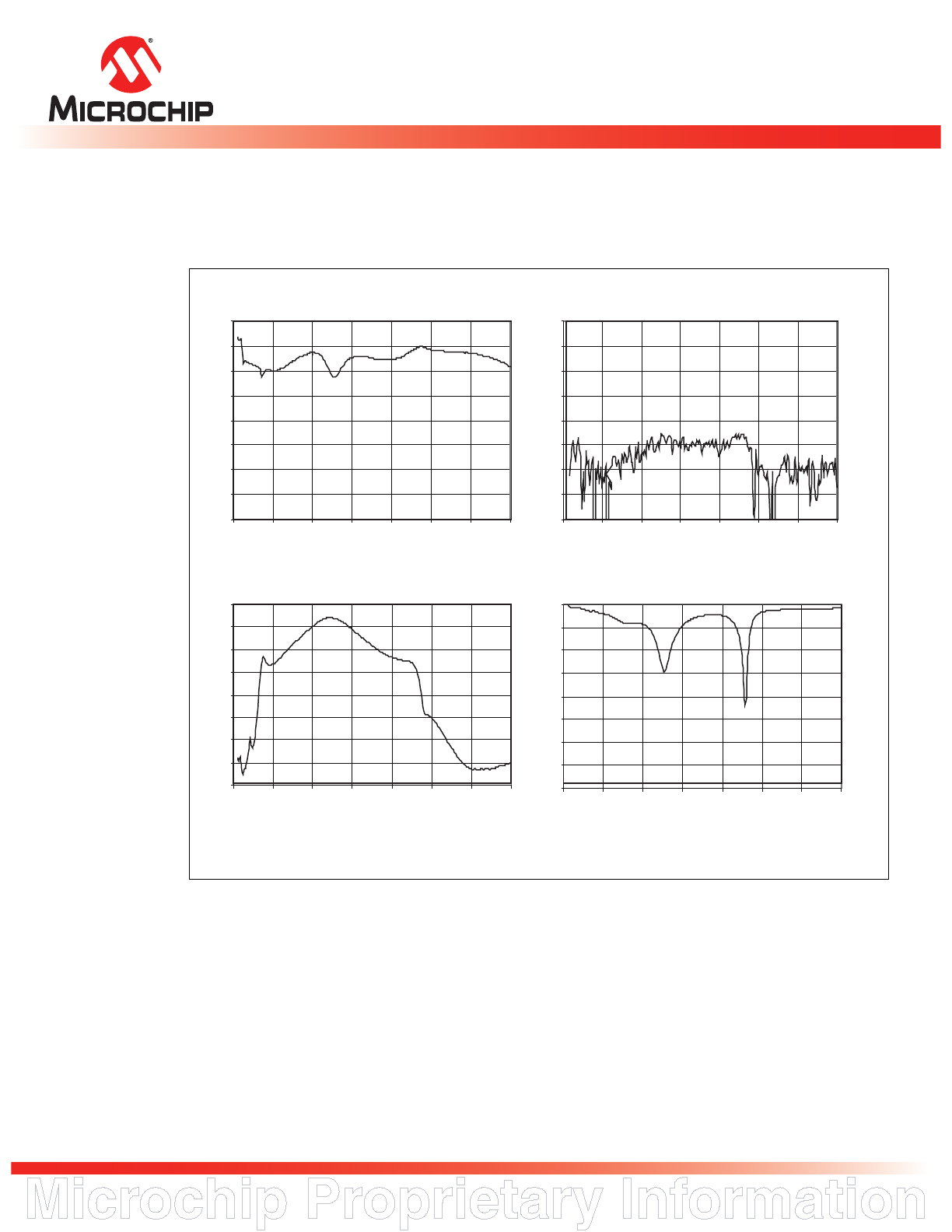
Figure 3: S-Parameters
1403 S-Parms.1.1
Frequency (GHz)
S11 (dB)
S12 versus Frequency
S12 (dB)
S11 versus Frequency
S21 versus Frequency
Frequency (GHz)
S21 (dB)
S22 versus Frequency
Frequency (GHz)
S22 (dB)
-40
-35
-30
-25
-20
-15
-10
-5
0
0.0
1.0
2.0
3.0
4.0
5.0
6.0
7.0
-80
-70
-60
-50
-40
-30
-20
-10
0
0.0
1.0
2.0
3.0
4.0
5.0
6.0
7.0
Frequency (GHz)
-40
-30
-10
0
10
20
30
40
0.0
1.0
2.0
3.0
4.0
5.0
6.0
7.0
-40
-35
-30
-25
-20
-15
-10
-5
0
0.0
1.0
2.0
3.0
4.0
5.0
6.0
7.0
Microchip Proprietary Information
©2013 Silicon Storage Technology, Inc.
DS75054A
01/13
8
2.4 GHz High-Power and High-Gain Power Amplifier
SST12CP11
Data Sheet
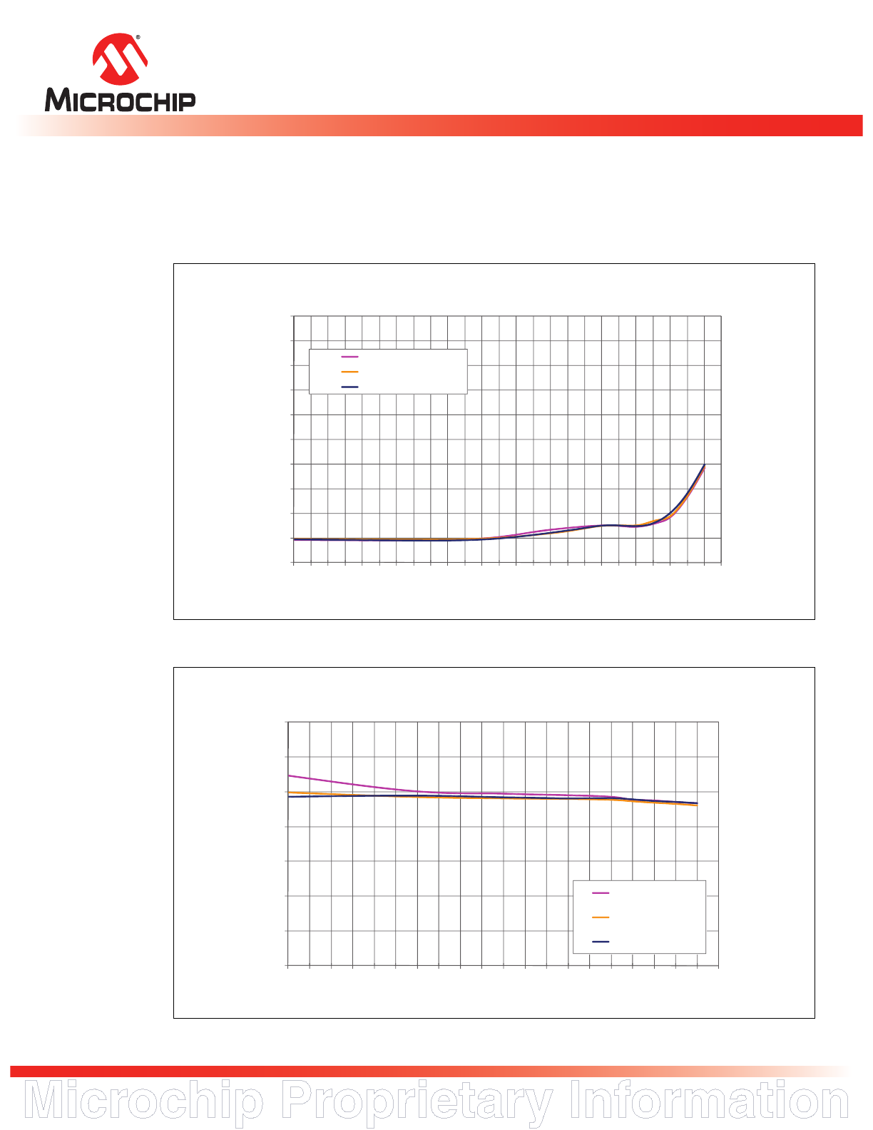
802.11ac Applications
Typical Performance Characteristics
Test Conditions: V
CC
= 5.0V, V
REG
= 3.20V, T
A
= 25°C, MCS8 signal, unless otherwise specified
Figure 4: EVM versus Output Power
Figure 5: Power Gain versus Output Power
75054 F21.0
0
1
2
3
4
5
6
7
8
9
10
0
1
2
3
4
5
6
7
8
9 10 11 12 13 14 15 16 17 18 19 20 21 22 23 24 25
EVM (%
)
Output Power (dBm)
EVM versus Output Power
Freq=2.412GHz
Freq=2.442GHz
Freq=2.472 GHz
75054 F22.0
20
22
24
26
28
30
32
34
5
6
7
8
9
10 11 12 13 14 15 16 17 18 19 20 21 22 23 24 25
P
o
we
r Ga
in (
d
B
)
Output Power (dBm)
Power Gain versus Output Power
Freq=2.412GHz
Freq=2.442GHz
Freq=2.472 GHz
Microchip Proprietary Information
©2013 Silicon Storage Technology, Inc.
DS75054A
01/13
9
2.4 GHz High-Power and High-Gain Power Amplifier
SST12CP11
Data Sheet
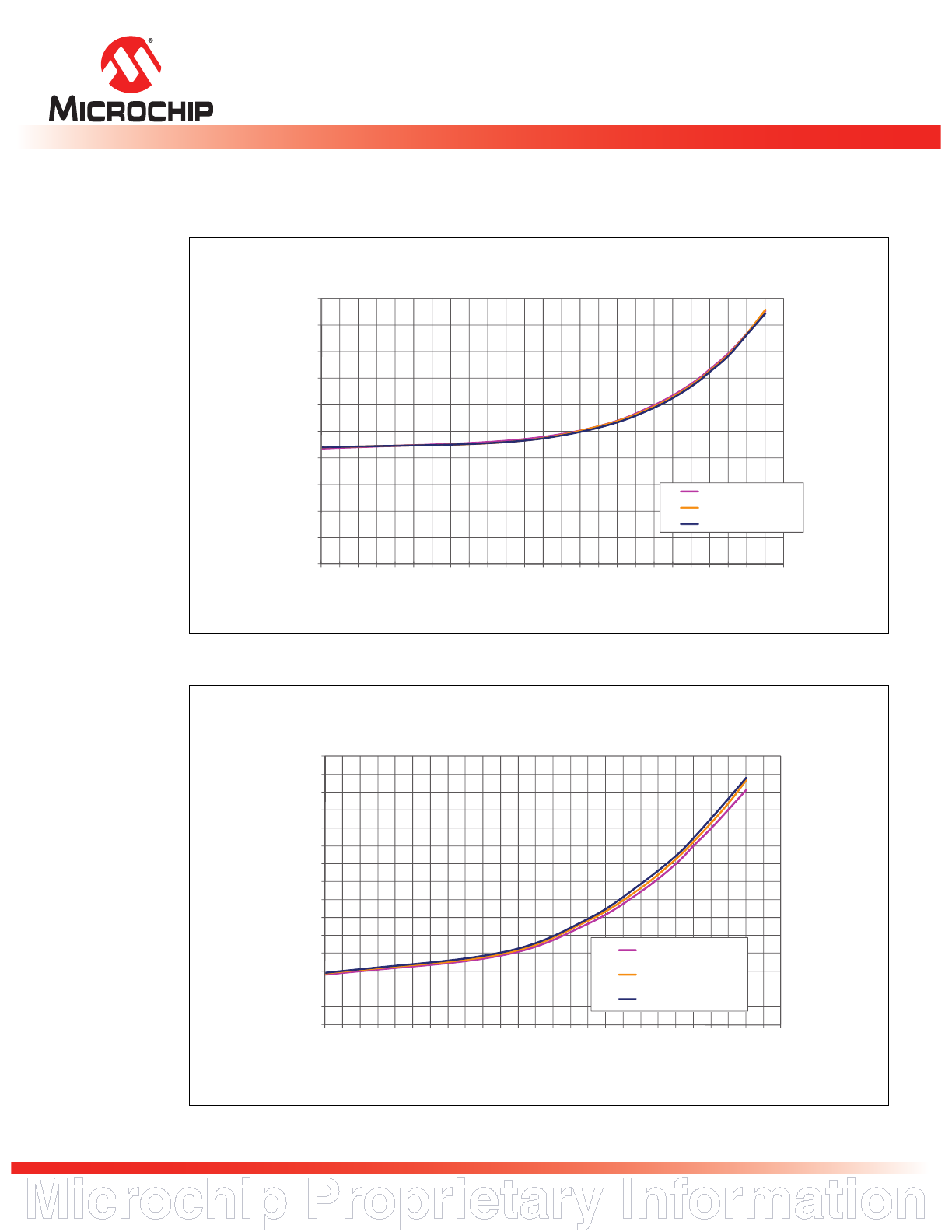
802.11ac Applications (continued)
Figure 6: Supply Current versus Output Power
Figure 7: Detector Characteristic versus Output Power
75054 F23.0
400
420
440
460
480
500
520
540
560
580
600
0
1
2
3
4
5
6
7
8
9 10 11 12 13 14 15 16 17 18 19 20 21 22 23 24 25
S
upply
C
ur
re
nt
(
m
A
)
Output Power (dBm)
Supply Current versus Output Power
Freq=2.412GHz
Freq=2.442GHz
Freq=2.472 GHz
75054 F24.0
0.00
0.10
0.20
0.30
0.40
0.50
0.60
0.70
0.80
0.90
1.00
1.10
1.20
1.30
1.40
1.50
0 1 2 3 4 5 6 7 8 9 10 11 12 13 14 15 16 17 18 19 20 21 22 23 24 25 26
Det
ect
o
r V
o
lt
ag
e (
V
)
Output Power (dBm)
Detector Voltage versus Output Power
Freq=2.412GHz
Freq=2.442GHz
Freq=2.472 GHz
Microchip Proprietary Information
©2013 Silicon Storage Technology, Inc.
DS75054A
01/13
10
2.4 GHz High-Power and High-Gain Power Amplifier
SST12CP11
Data Sheet
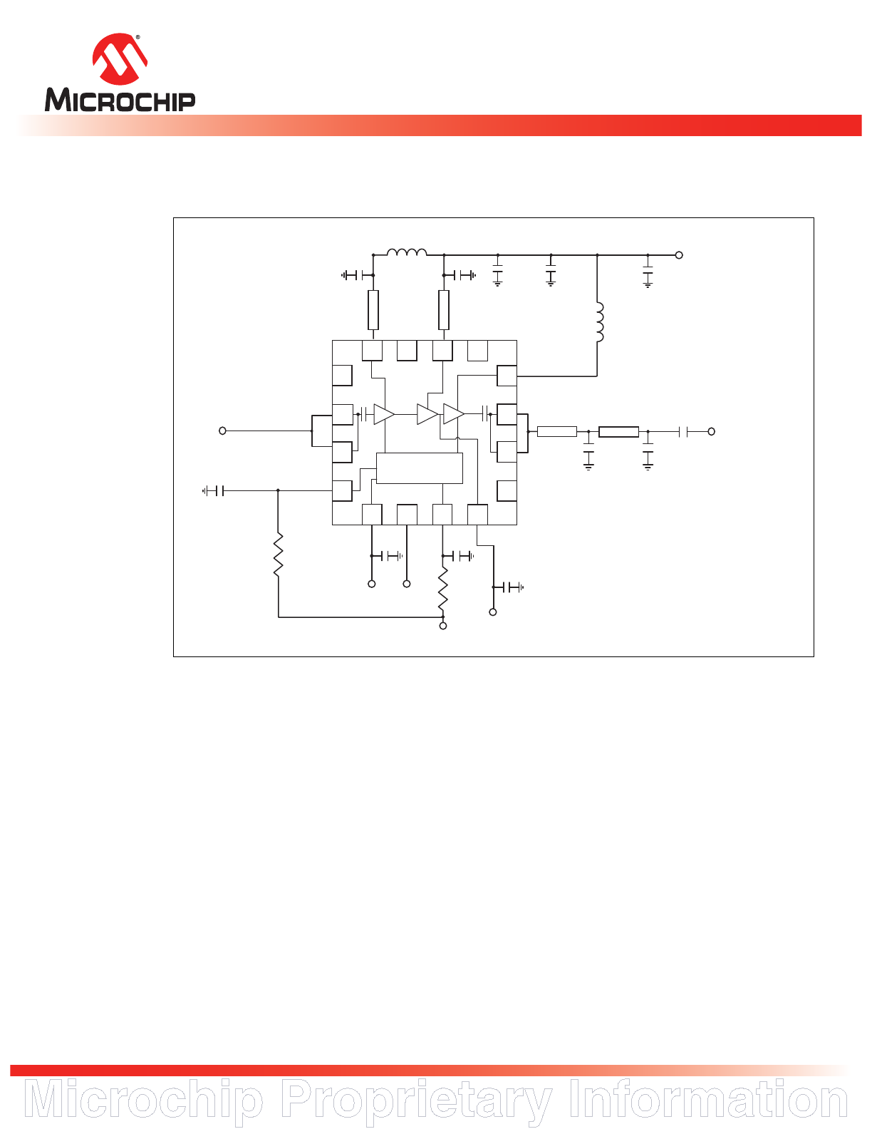
802.11ac Applications (continued)
Figure 8: Typical Schematic for 802.11ac Applications
2
5
6
7
8
9
11
16
15
1
50
Ω
1.8 pF
50
Ω
/110 mil
50
Ω
GND
VREG
14
13
0.1 µF
Vcc
4
12
10
0.1 µF
6.8
Ω
3
DNI
VDET
75054 Schematic.3.0
Suggested operation conditions:
1. V
CC
= 5.0V/ V
REG
= 3.2V
2. Center slug to RF ground
0.1 µF
VCC
12 nH (0805 size)
1000 pF
4.7 nH
50
Ω
/30mil
1.2 pF
8.2 pF
0.1 µF
0.1 µF
56
Ω
Bias Circuit
4.7 µF
0.1 µF
50
Ω
/90 mil
50
Ω
/90 mil