

PR
OPRIET
AR
Y AND
CONFIDENTIAL
A Microchip Technology Company
©2011 Silicon Storage Technology, Inc.
DS75040A
12/11
Data Sheet
www.microchip.com
Features
• Gain:
– Typically 12 dB gain across 2.4–2.5 GHz for Receiver
(RX) chain.
– Typically 29 dB gain across 2.4–2.5 GHz over temperature
0°C to +80°C for Transmitter (TX) chain.
• Low-Noise Figure
– Typical 1.45 dB across 2.4–2.55 GHz
• 50
Input/Output matched along RX chain.
• Rx IIP3
– >1 dbm across 2.4–2.55 GHz
• High linear output power:
– >26.5 dBm P1dB
– Meets 802.11g OFDM ACPR requirement up to 23 dBm
– ~3% added EVM up to 19 dBm for
54 Mbps 802.11g signal
– Meets 802.11b ACPR requirement up to 24 dBm
• High power-added efficiency/Low operating cur-
rent for both 802.11g/b applications
– ~22%/210 mA @ P
OUT
= 22 dBm for 802.11g
– ~26%/240 mA @ P
OUT
= 23.5 dBm for 802.11b
• Low idle current
– ~70 mA I
CQ
• Low shut-down current (Typical 2.5 µA)
• Built-in, Ultra-low I
REF
power-up/down control
– I
REF
<4 mA
• High-speed power-up/down
– Turn on/off time (10%- 90%) <100 ns
– Typical power-up/down delay with driver delay included
<200 ns
• High temperature stability
– ~1 dB gain/power variation between 0°C to +85°C
• Simple input/output matching
• Single positive power supply
• Packages available
– 24-contact WQFN – 4mm x 4mm
• All devices are RoHS compliant
Applications
• WLAN
• Bluetooth
• Wireless Network
2.4 GHz Front-End Module
SST12LF01
The SST12LF01 is a 2.4 GHz Front-End Module (FEM) that combines a high-per-
formance Low-Noise Amplifier (LNA) and a Power Amplifier (PA). Designed in
compliance with IEEE 802.11 b/g/n applications and based on GaAs PHEMT/HBT
technology, the SST12LF01 operates within the frequency range of 2.4- 2.55 GHz
at a very low DC-current consumption. The Transmitter chain has excellent linear-
ity, typically <3% added EVM up to 19 dBm output power, which is essential for 54
Mbps 802.11g operation while meeting 802.11g spectrum mask at 23 dBm. The
SST12LF01 is offered in a 24-contact WQFN package.

PR
OPRIET
AR
Y AND
CONFIDENTIAL
©2011 Silicon Storage Technology, Inc.
DS75040A
12/11
2
2.4 GHz Front-End Module
SST12LF01
Data Sheet
A Microchip Technology Company
Product Description
The SST12LF01 is a 2.4 GHz Front-End Module (FEM) that combines a high-performance Low-Noise
Amplifier (LNA) and a Power Amplifier (PA).
Designed in compliance with IEEE 802.11 b/g/n applications and based on GaAs PHEMT/HBT tech-
nology, the SST12LF01 operates within the frequency range of 2.4–2.55 GHz at a very low DC-current
consumption. There are two components to the FEM: the Receiver (RX) chain and the Transmitter
(TX) chain.
The RX chain consist of a cost effective Low-Noise Amplifier (LNA) cell which requires no external RF-
matching components. This device is based on the 0.5m GaAs PHEMT technology, and complies with
802.11 b/g/n applications.
The LNA provides high-performance, low-noise, and moderate gain operation within the 2.4–2.55 GHz
frequency band. Across this frequency band, the LNA typically provides 12 dB gain and 1.45 dB noise
figure.
This LNA cell is designed with a self DC-biasing scheme, which maintains low DC current consump-
tion, nominally at 11 mA, during operation. Optimum performance is achieved with only a single power
supply and no external bias resistors or networks are required. The input and output ports are singled-
ended 50 Ohm matched. RF ports are also DC isolated requiring no dc blocking capacitors or match-
ing components to reduce system board Bill of Materials (BOM) cost.
The TX chain includes a high-efficiency PA based on InGaP/GaAs HBT technology. The PA typically
provides 30 dB gain with 22% power-added efficiency at P
OUT
= 22 dBm for 802.11g and 27% power-
added efficiency at P
OUT
= 24 dBm for 802.11b.
The Transmitter chain has excellent linearity, typically <4% added EVM up to 20 dBm output power,
which is essential for 54 Mbps 802.11g operation while meeting 802.11g spectrum mask at 23 dBm.
The SST12LF01 is offered in 24-contact WQFN package. See Figure 2 for pin assignments and Table 1
for pin descriptions.
PR
OPRIET
AR
Y AND
CONFIDENTIAL
©2011 Silicon Storage Technology, Inc.
DS75040A
12/11
3
2.4 GHz Front-End Module
SST12LF01
Data Sheet
A Microchip Technology Company
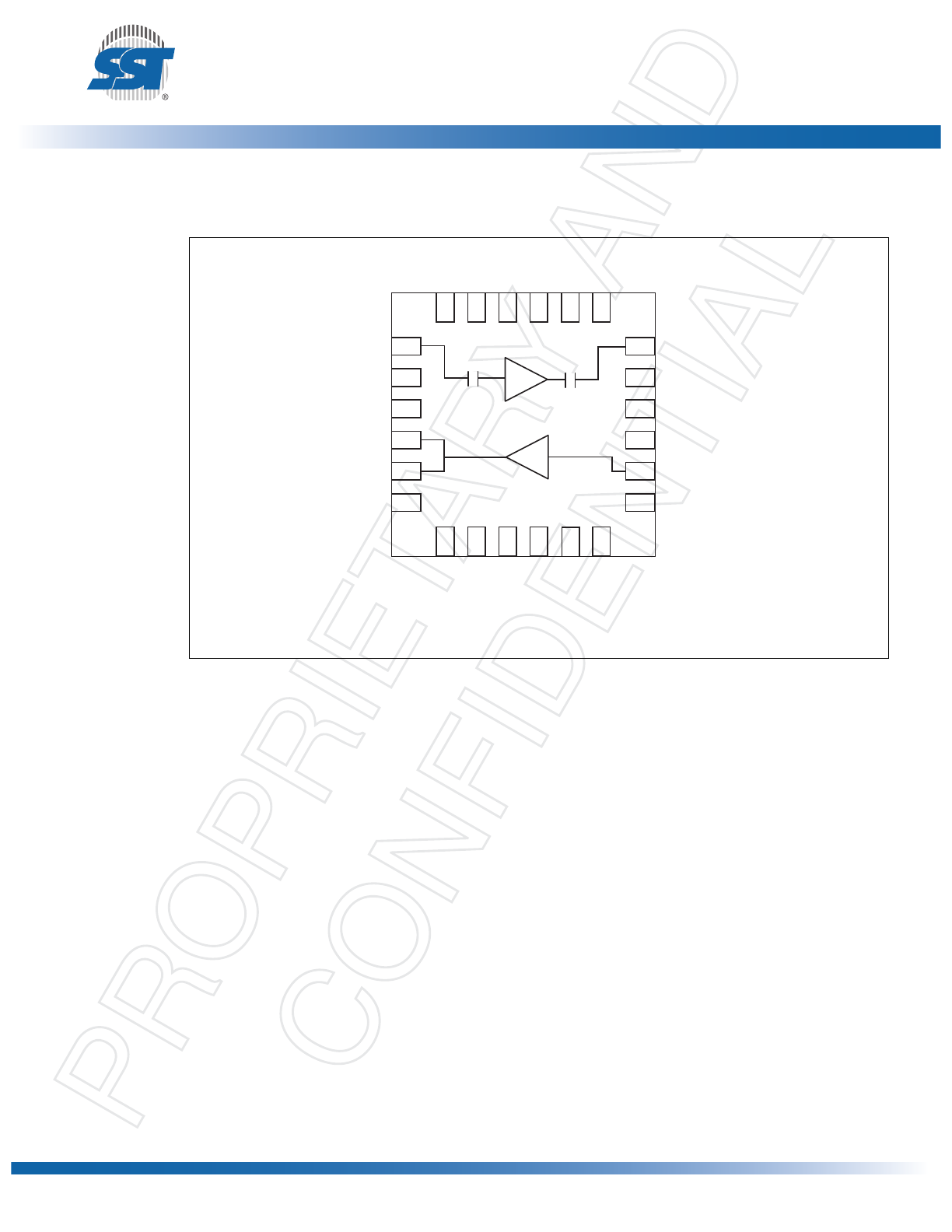
Functional Blocks
Figure 1: Functional Block Diagram
2
5
6
8
16
15
1
14
4
9
11
12
10
13
3
7
17
18
19
20
21
22
23
24
1330 B1.1
LNA
PA
DC Block
DC Block
PR
OPRIET
AR
Y AND
CONFIDENTIAL
©2011 Silicon Storage Technology, Inc.
DS75040A
12/11
4
2.4 GHz Front-End Module
SST12LF01
Data Sheet
A Microchip Technology Company
Pin Assignments
Figure 2: Pin Assignments for 24-contact WQFN
2
5
6
8
16
15
1
14
4
9
11
12
10
13
V
REF
NC
V
CCb
NC
NC
V
DD
_RX
3
NC
LNA
IN
NC
7
1330 P1.1
17
18
19
20
21
22
23
24
Top View
(contacts facing down)
RF and DC GND
0
PA
OUT
V
CC
_TX2
LNA
OUT
PA
IN
NC
V
CC
_TX1
NC
NC
NC
NC
NC
NC
NC
NC
PA
OUT
PR
OPRIET
AR
Y AND
CONFIDENTIAL
©2011 Silicon Storage Technology, Inc.
DS75040A
12/11
5
2.4 GHz Front-End Module
SST12LF01
Data Sheet
A Microchip Technology Company
Pin Descriptions
Table 1: Pin Description
Symbol
Pin No.
Pin Name
Type
1
1. I=Input, O=Output
Function
LNA
IN
1
I
LNA RF Input
NC
2
No Connection
Unconnected pin
NC
3
No Connection
Unconnected pin
PA
OUT
4
O
PA RF output
PA
OUT
5
O
PA RF output
V
CC
_TX2
6
Power Supply
PWR
PA power supply, 2
nd
stage
NC
7
No Connection
Unconnected pin
NC
8
No Connection
Unconnected pin
V
CC
_TX1
9
Power Supply
PWR
PA power supply,1
st
stage
V
REF
10
PWR
PA-enable and current control
V
CCb
11
Power Supply
PWR
PA power supply, bias circuit
NC
12
No Connection
Unconnected pin
NC
13
No Connection
Unconnected pin
PA
IN
14
I
PA RF input
NC
15
No Connection
Unconnected pin
NC
16
No Connection
Unconnected pin
NC
17
No Connection
Unconnected pin
LNA
OUT
18
O
LNA RF Output
NC
19
No Connection
Unconnected pin
NC
20
No Connection
Unconnected pin
NC
21
No Connection
Unconnected pin
V
DD
_RX
22
Power Supply
PWR
LNA power supply
NC
23
No Connection
Unconnected pin
NC
24
No Connection
Unconnected pin
T1.0 75040
PR
OPRIET
AR
Y AND
CONFIDENTIAL
©2011 Silicon Storage Technology, Inc.
DS75040A
12/11
6
2.4 GHz Front-End Module
SST12LF01
Data Sheet
A Microchip Technology Company
Electrical Specifications
The AC and DC specifications for the power amplifier interface signals. Refer to Table 3 for the DC voltage and
current specifications. Refer to Figures 3 through 14 for the RF performance.
Absolute Maximum Stress Ratings (Applied conditions greater than those listed under “Absolute
Maximum Stress Ratings” may cause permanent damage to the device. This is a stress rating only and
functional operation of the device at these conditions or conditions greater than those defined in the
operational sections of this data sheet is not implied. Exposure to absolute maximum stress rating con-
ditions may affect device reliability.)
Input power to pins 1 (LNA) . . . . . . . . . . . . . . . . . . . . . . . . . . . . . . . . . . . . . . . . . . . . . . . . . . . . 0 dBm
Input power to pins 14 (PA) . . . . . . . . . . . . . . . . . . . . . . . . . . . . . . . . . . . . . . . . . . . . . . . . . . . . -5 dBm
Average output power pins 4 and 5 (P
OUT
)
1
. . . . . . . . . . . . . . . . . . . . . . . . . . . . . . . . . . . . . . 24 dBm
1. Never measure with CW source. Pulsed single-tone source with <50% duty cycle is recommended. Exceeding the max-
imum rating of average output power could cause permanent damage to the device.
Average output power pin 18 (P
OUT
)
1
. . . . . . . . . . . . . . . . . . . . . . . . . . . . . . . . . . . . . . . . . . . . 9 dBm
Supply Voltage at pins 6, 9, and 11 (V
CC
) . . . . . . . . . . . . . . . . . . . . . . . . . . . . . . . . . . . -0.3V to +4.6V
Supply Voltage at pin 22 (V
DD
) . . . . . . . . . . . . . . . . . . . . . . . . . . . . . . . . . . . . . . . . . . . -0.3V to +4.6V
Reference voltage to pin 10 (V
REF
) . . . . . . . . . . . . . . . . . . . . . . . . . . . . . . . . . . . . . . . . -0.3V to +3.6V
DC supply current to pin 10 (I
DD
) . . . . . . . . . . . . . . . . . . . . . . . . . . . . . . . . . . . . . . . . . . . . . . . . 14 mA
DC supply current to pin 6, 9, and 11 (I
CC
) . . . . . . . . . . . . . . . . . . . . . . . . . . . . . . . . . . . . . . . 300 mA
Operating Temperature (T
A
) . . . . . . . . . . . . . . . . . . . . . . . . . . . . . . . . . . . . . . . . . . . . -40ºC to +85ºC
Storage Temperature (T
STG
) . . . . . . . . . . . . . . . . . . . . . . . . . . . . . . . . . . . . . . . . . . . -40ºC to +120ºC
Maximum Junction Temperature (T
J
) . . . . . . . . . . . . . . . . . . . . . . . . . . . . . . . . . . . . . . . . . . . +150ºC
Surface Mount Solder Reflow Temperature . . . . . . . . . . . . . . . . . . . . . . . . . . . 260°C for 10 seconds
Table 2: Operating Range
Range
Ambient Temp
V
CC
/ V
DD
Commercial
-0 to 80ºC
2.9–4.2V
T2.1 75040
Table 3: DC Electrical Characteristics
Symbol
Parameter
Min.
Typ
Max.
Unit
V
CC
Supply Voltage at pins 6, 9, 11, and 22
3.3
4.2
V
I
CC
Supply Current at pin 22
10
mA
for 802.11g, 22 dBm at pins 6, 9, and 11
210
mA
for 802.11b, 23.5 dBm at pins 6, 9, and 11
260
mA
I
CQ
Idle current for 802.11g to meet EVM<4% @ 20 dBm
75
mA
I
OFF
Shut down current
2.5
µA
V
REF
1
1. V
REF
and V
REG
are defined in Figure 15. Three combinations of resistor values and applied voltages of V
REG
are sug-
gested in Table 3.
Reference Voltage at pin10 with R
REG
= 0
resistor
2.7
V
Reference Voltage at pin 10 with R
REG
= 120
resistor
2.7
2.9
3.1
V
Reference Voltage at pin 10 with R
REG
= 220
resistor
2.9
3.1
3.3
V
T3.1 75040
PR
OPRIET
AR
Y AND
CONFIDENTIAL
©2011 Silicon Storage Technology, Inc.
DS75040A
12/11
7
2.4 GHz Front-End Module
SST12LF01
Data Sheet
A Microchip Technology Company
Table 4: AC Electrical Characteristics for RX Chain
Symbol
Parameter
Min.
Typ
Max.
Unit
F
L-U
Frequency range
2400
2550
MHz
G
Small signal gain
10
12
dB
NF
Noise Figure
1.45
dB
IIP3
2.4–2.55 GHz
1
3
dBm
T4.1 75040
Table 5: AC Electrical Characteristics for TX Chain
Symbol
Parameter
Min.
Typ
Max.
Unit
F
L-U
Frequency range
2400
2485
MHz
P
OUT
Output power
@ PIN = -6 dBm 11b signals
23
dBm
@ PIN = -9 dBm 11g signals
20
dBm
G
Small signal gain
28
29
33
dB
G
VAR1
Gain variation over band (2400~2485 MHz)
±0.5
dB
G
VAR2
Gain ripple over channel (20 MHz)
0.2
dB
ACPR
Meet 11b spectrum mask
23
dBm
Meet 11g OFDM 54 Mbps spectrum mask
22
dBm
Added EVM @ 20 dBm output with 11g OFDM 54 Mbps signal
4
%
2f, 3f, 4f, 5f
Harmonics at 22 dBm, without external filters
-40
dBc
T5.1 75040
PR
OPRIET
AR
Y AND
CONFIDENTIAL
©2011 Silicon Storage Technology, Inc.
DS75040A
12/11
8
2.4 GHz Front-End Module
SST12LF01
Data Sheet
A Microchip Technology Company
Typical Performance Characteristics
Test Conditions: V
DD
= 3.0V, T
A
= 25°C, unless otherwise specified
Figure 3: S-Parameters, RX Chain
Frequency (GHz)
Frequency (GHz)
S11 versus Frequency
S12 versus Frequency
S22 versus Frequency
S21 versus Frequency
1330-sparm1.3
Frequency (GHz)
-40
-30
-20
-10
0
10
20
0
1
2
3
4
5
6
7
8
9
10
Frequency (GHz)
S11 (dB)
-60
-50
-40
-30
-20
-10
0
10
20
0
2
4
6
8
10
S12 (dB)
1
3
5
7
9
S21 (dB)
-40
-35
-30
-25
-20
-15
-10
-5
0
0
2
4
6
8
10
S22 (dB)
1
3
5
7
9
-50
-40
-30
-20
-10
0
10
20
0
1
2
3
4
5
6
7
8
9
10
PR
OPRIET
AR
Y AND
CONFIDENTIAL
©2011 Silicon Storage Technology, Inc.
DS75040A
12/11
9
2.4 GHz Front-End Module
SST12LF01
Data Sheet
A Microchip Technology Company
Figure 4: Noise Figure versus Frequency, RX Chain
Frequency (GHz)
1330 F8.1
0
0.5
1.0
1.5
2.0
2.5
3.0
1.5
2.0
2.5
3.0
Frequency (GHz)
Noise Figure (dB)
Temp = -10 degree
Temp = 25 degree
Temp = 80 degree
PR
OPRIET
AR
Y AND
CONFIDENTIAL
©2011 Silicon Storage Technology, Inc.
DS75040A
12/11
10
2.4 GHz Front-End Module
SST12LF01
Data Sheet
A Microchip Technology Company
Figure 5: Frequency Response of Gain (S21) over three Temperatures
1330 F12.1
-15
-10
-5
0
5
10
15
20
1
2
3
4
Frequency (GHz)
Ga
in
(d
B
)
Tem p = - 10 degree
Room temp
Tem p = 80 degree