

Microchip Proprietary Information
©2012 Silicon Storage Technology, Inc.
DS75032A
10/12
Data Sheet
www.microchip.com
Features
• High Gain:
– Typically 29 dB gain across 2.4-2.5 GHz
– Typically 29-26 dB gain across 4.9-5.8 GHz10/12
• High linear output power:
– >25 dBm P1dB (Pulsed single-tone signal) across 2.4-2.5
GHz
– Meets 802.11b OFDM ACPR requirement up to 23.5
dBm across 2.4-2.5 GHz
– Meets 802.11g OFDM ACPR requirement up to 23 dBm
across 2.4-2.5 GHz
– Added EVM ~4% up to 19 dBm for
54 Mbps 802.11g signal across 2.4-2.5 GHz
– >24 dBm P1dB across 4.9-5.8 GHz
– Meets 802.11a OFDM ACPR requirement up to 22.5
dBm across 4.9-5.8 GHz
– Added EVM ~4% up to 18 dBm for
54 Mbps 802.11a signal across 4.9-5.8 GHz
• High power-added efficiency/Low operating cur-
rent for 802.11a/b/g applications
– ~160 mA @ P
OUT
= 19 dBm for 802.11g
– ~235 mA @ P
OUT
= 23.5 dBm for 802.11b
– ~270 mA @ P
OUT
= 18 dBm for 802.11a
• Built-in Ultra-low I
REF
power-up/down control
– I
REF
< 2 mA
• High-speed power-up/down
– Turn on/off time (10%-90%) <100 ns
– Typical power-up/down delay with driver delay included
<200 ns
• High temperature stability
– ~1 dB gain/power variation between 0°C to +85°C across
2.4-2.5 GHz
– ~3/1 dB gain/max linear power variation between 0°C to
+85°C across 4.9-5.8 GHz
– ±0.5 dB detector variation between 0°C to +85°C
• Low shut-down current (< 2 µA)
• 20 dB dynamic range on-chip power detection
• Built-in input/output matching
• Packages available
– 16-contact LGA package (4mm x 4mm)
• All non-Pb (lead-free) devices are ROHS compliant.
Applications
• WLAN (IEEE 802.11a/g/b)
• Japanese WLAN
• HyperLAN2
• Multimedia
• Home RF
• Cordless phones
2.4-2.5 GHz / 4.9-5.8 GHz Dual-Band Power Amplifier Module
SST13LP05
The SST13LP05 is a fully matched, dual-band power amplifier module (PAM) based
on the highly-reliable InGaP/GaAs HBT technology. This PAM provides excellent
RF performance, temperature-stable power detectors, and low-current analog on/
off control interfaces. The SST13LP05 provides stable RF and power detector per-
formance over a large VCC power supply variation, with an ultra-low shut-down cur-
rent. The SST13LP05 is ideal for the final stage power amplification in both battery-
powered 802.11a/b/g WLAN transmitters and access point applications.

Microchip Proprietary Information
©2012 Silicon Storage Technology, Inc.
DS75032A
10/12
2
2.4-2.5 GHz / 4.9-5.8 GHz Dual-Band Power Amplifier
SST13LP05
Data Sheet
Product Description
The SST13LP05 is a fully matched, dual-band power amplifier module (PAM) based on the highly-reli-
able InGaP/GaAs HBT technology. This PAM provides excellent RF performance, temperature-stable
power detectors, and low-current analog on/off control interfaces. The SST13LP05 provides stable RF
and power detector performance over a large V
CC
power supply variation, with an ultra-low shut-down
current.
With a near-zero Rest of Bill of Materials (RBOM), the SST13LP05 is designed for 802.11a/b/g appli-
cations covering frequency bands 2.4-2.5 GHz and 4.9-5.8 GHz for U.S., European, and Japanese
markets.
The SST13LP05 has excellent linearity, typically 4% added Error Vector Magnitude (EVM) at 19 dBm
output power. This output power is essential for 54 Mbps 802.11g operation while meeting 802.11g
spectrum mask at 23 dBm and 802.11b spectrum mask at 23.5 dBm. For 802.11a operation, the
SST13LP05 typically demonstrates <4% added EVM at 18 dBm output power while meeting 802.11a spec-
trum mask at 22.5 dBm.
The SST13LP05 also has wide-range (>20 dB), temperature-stable (±0.5 dB across 0°C to +85°C),
directionally-coupled, power detectors which provide a reliable and cost-effective solution to board-
level power control. The device’s analog on/off control can be driven by an analog or digital control sig-
nal from either a transceiver or baseband chip.
These features, coupled with low operating current, make the SST13LP05 ideal for the final stage
power amplification in both battery-powered 802.11a/b/g WLAN transmitters and access point applica-
tions.
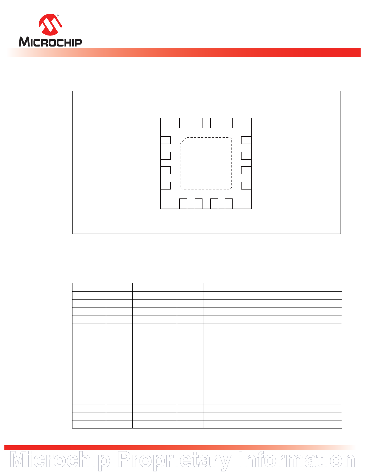
The SST13LP05 is offered in a 16-contact LGA package. See Figure 2 for pin assignments and Table 1
for pin descriptions.
Microchip Proprietary Information
©2012 Silicon Storage Technology, Inc.
DS75032A
10/12
3
2.4-2.5 GHz / 4.9-5.8 GHz Dual-Band Power Amplifier
SST13LP05
Data Sheet
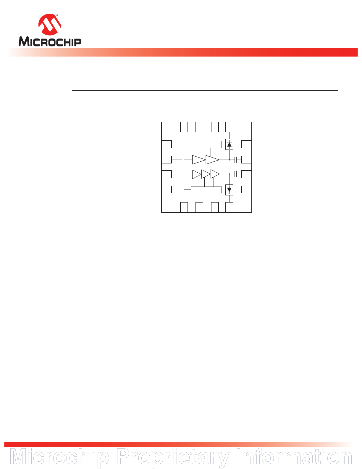
Functional Blocks
Figure 1: Functional Block Diagram
V
REG
_LB
V
CC
_LB
NC
Det_LB
V
REG
_HB
NC
V
CC
_HB
Det_HB
NC
RF
OUT
_LB
RF
OUT
_HB
NC
NC
RF
IN
_LB
RF
IN
_HB
NC
1318 B1.0
5
6
8
16
15
14
9
11
12
10
13
2
1
4
3
7
Bias Network
Bias Network
Microchip Proprietary Information
©2012 Silicon Storage Technology, Inc.
DS75032A
10/12
4
2.4-2.5 GHz / 4.9-5.8 GHz Dual-Band Power Amplifier
SST13LP05
Data Sheet
Pin Assignments
Figure 2: Pin Assignments for 16-contact LGA
Pin Descriptions
Table 1: Pin Description
Symbol
Pin No.
Pin Name
Type
Function
GND
0
Ground
Ground Pad
NC
1
No Connection
Unconnected Pin
RF
IN
_LB
2
I
50
Matched RF Input for Low Band, AC coupled
RF
IN
_HB
3
I
50
Matched RF Input for High Band, AC coupled
NC
4
No Connection
Unconnected Pin
V
REG
_HB
5
Power Supply
PWR
Analog current control for High Band
NC
6
No Connection
Unconnected Pin
V
CC
_HB
7
Power Supply
PWR
V
CC
Power Supply for High Band
D
ET
_HB
8
O
Detector Voltage Output for High Band
NC
9
No Connection
Unconnected Pin
RF
OUT
_HB
10
Power Supply
O/PWR
50
Matched RF output for High Band
RF
OUT
_LB
11
Power Supply
O/PWR
50
Matched RF output for Low Band
NC
12
No Connection
Unconnected Pin
D
ET
_LB
13
O
Detector Voltage Output for Low Band
V
CC
_LB
14
Power Supply
PWR
V
CC
Power Supply for Low Band
NC
15
No Connection
Unconnected Pin
V
REG
_LB
16
Power Supply
PWR
Analog current control for Low Band
T1.0 75032
V
REG
_LB
V
CC
_LB
NC
Det_LB
V
REG
_HB
NC
V
CC
_HB
Det_HB
NC
RF
OUT
_LB
RF
OUT
_HB
NC
NC
RF
IN
_LB
RF
IN
_HB
NC
1318 P1.1
5
6
8
16
15
14
9
11
12
10
13
2
1
4
3
7
Top View
(contacts facing down)
RF and DC GND
0
Microchip Proprietary Information
©2012 Silicon Storage Technology, Inc.
DS75032A
10/12
5
2.4-2.5 GHz / 4.9-5.8 GHz Dual-Band Power Amplifier
SST13LP05
Data Sheet
Electrical Specifications
The AC and DC specifications for the power amplifier interface signals. Refer to Tables 2 and 4 for the DC volt-
age and current specifications. Refer to Figures 3 through 22 for the RF performance.
For 802.11b/g Operation
Absolute Maximum Stress Ratings Applied conditions greater than those listed under “Absolute Maxi-
mum Stress Ratings” may cause permanent damage to the device. This is a stress rating only and functional
operation of the device at these conditions or conditions greater than those defined in the operational sections
of this data sheet is not implied. Exposure to absolute maximum stress rating conditions may affect device reli-
ability.
Supply Voltage (V
CC
) . . . . . . . . . . . . . . . . . . . . . . . . . . . . . . . . . . . . . . . . . . . . . . . . . . . -0.3V to +3.6V
Reference Voltage (V
REF
) . . . . . . . . . . . . . . . . . . . . . . . . . . . . . . . . . . . . . . . . . . . . . . . -0.3V to +3.3V
DC supply current (I
CC
) . . . . . . . . . . . . . . . . . . . . . . . . . . . . . . . . . . . . . . . . . . . . . . . . . . . . . . 400 mA
Operating Temperature (T
A
) . . . . . . . . . . . . . . . . . . . . . . . . . . . . . . . . . . . . . . . . . . . . -40ºC to +85ºC
Storage Temperature (T
STG
) . . . . . . . . . . . . . . . . . . . . . . . . . . . . . . . . . . . . . . . . . . . -40ºC to +120ºC
Maximum Junction Temperature (T
J
) . . . . . . . . . . . . . . . . . . . . . . . . . . . . . . . . . . . . . . . . . . . +150ºC
Table 2: DC Electrical Characteristics
Symbol
Parameter
Min.
Typ
Max.
Unit
V
CC
Supply Voltage
3.0
3.3
3.6
V
I
CC
Supply Current
for 802.11g, 19 dBm
160
mA
for 802.11b, 23.5 dBm
235
mA
I
REG
Analog control current at On state
2
mA
V
REG
Reference Voltage
2.95
V
T2.0 75032
Table 3: AC Electrical Characteristics for Configuration
Symbol
Parameter
Min.
Typ
Max.
Unit
F
L-U
Frequency range
2.4
2.5
GHz
G
Small signal gain
28
29
dB
G
VAR1
Gain variation over temperature 0
°
C – 85
°
C
-1
1
dB
G
VAR2
Gain flatness over any 50 MHz bandwidth
-0.3
0.3
dB
ACPR
Meet 11b spectrum mask
22
23
dBm
Meet 11g OFDM 54 Mbps spectrum mask
22
23
dBm
Added EVM P
OUT
= 19 dBm with 54Mbps
-28
dB
11g OFDM signal when operating at 3.3V Vcc
4
%
2f, 3f, 4f, 5f
Harmonics at P
OUT
= 20 dBm
-50
dBc
Spurious non-harmonics at P
OUT
= 20 dBm
-60
dBc
In/Out return loss at 50
nominal impedance
6
dB
T3.0 75032
Microchip Proprietary Information
©2012 Silicon Storage Technology, Inc.
DS75032A
10/12
6
2.4-2.5 GHz / 4.9-5.8 GHz Dual-Band Power Amplifier
SST13LP05
Data Sheet
For 802.11a Operation
Table 4: DC Electrical Characteristics
Symbol
Parameter
Min.
Typ
Max.
Unit
V
CC
Supply Voltage
3
3.3
3.6
V
I
CC
Supply Current
for 802.11a, 18 dBm
270
mA
I
REG
Analog control current at On state
2
A
V
REG
Reference Voltage
2.95
V
T4.1 75032
Table 5: AC Electrical Characteristics for Configuration
Symbol
Parameter
Min.
Typ
Max.
Unit
F
L-U
Frequency range
4.92
5.805
GHz
G
Small signal gain across 4.9- 5.8 GHz
26
dB
G
VAR1
Gain variation over temperature 0
°
C – 85
°
C
-1
1
dB
G
VAR2
Gain flatness over any 100 MHz bandwidth
-0.5
0.5
dB
ACPR
Meet 11a OFDM 54 Mbps spectrum mask
22
22.5
dBm
Added EVM
P
OUT
= 18 dBm with 54Mbps
-28
dB
11aOFDM signal when operating at 3.3V Vcc
4
%
2f, 3f, 4f, 5f
Harmonics at 20 dBm
-45
dBc
T5.1 75032
Microchip Proprietary Information
©2012 Silicon Storage Technology, Inc.
DS75032A
10/12
7
2.4-2.5 GHz / 4.9-5.8 GHz Dual-Band Power Amplifier
SST13LP05
Data Sheet
Typical Low Band Performance for 802.11b/g
Test Conditions: V
CC
= 3.3V, T
A
= 25°C, V
REF
= 2.95V unless otherwise noted
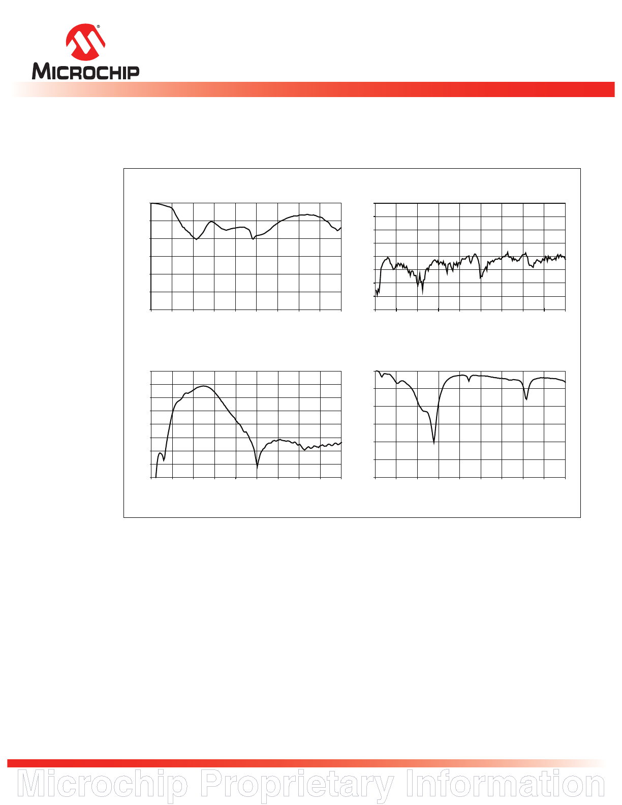
Figure 3: Low Band S-Parameters
1318 SParmLowB.0
S11 versus Frequency
-30
-25
-20
-15
-10
-5
0
0.0
1.0
2.0
3.0
4.0
5.0
6.0
7.0
8.0
9.0
Frequency (GHz)
S11
(dB)
S12 versus Frequency
-80
-70
-60
-50
-40
-30
-20
-10
0
0.0
1.0
2.0
3.0
4.0
5.0
6.0
7.0
8.0
9.0
Frequency (GHz)
S12
(dB)
S21 versus Frequency
-40
-30
-20
-10
0
10
20
30
40
0.0
1.0
2.0
3.0
4.0
5.0
6.0
7.0
8.0
9.0
Frequency (GHz)
S21
(dB)
S22 versus Frequency
-30
-25
-20
-15
-10
-5
0
0.0
1.0
2.0
3.0
4.0
5.0
6.0
7.0
8.0
9.0
Frequency (GHz)
S22
(dB)
Microchip Proprietary Information
©2012 Silicon Storage Technology, Inc.
DS75032A
10/12
8
2.4-2.5 GHz / 4.9-5.8 GHz Dual-Band Power Amplifier
SST13LP05
Data Sheet
Test Conditions: V
CC
= 3.3 V, V
REF
= 2.95 V, 54 Mbps 802.11g OFDM signal
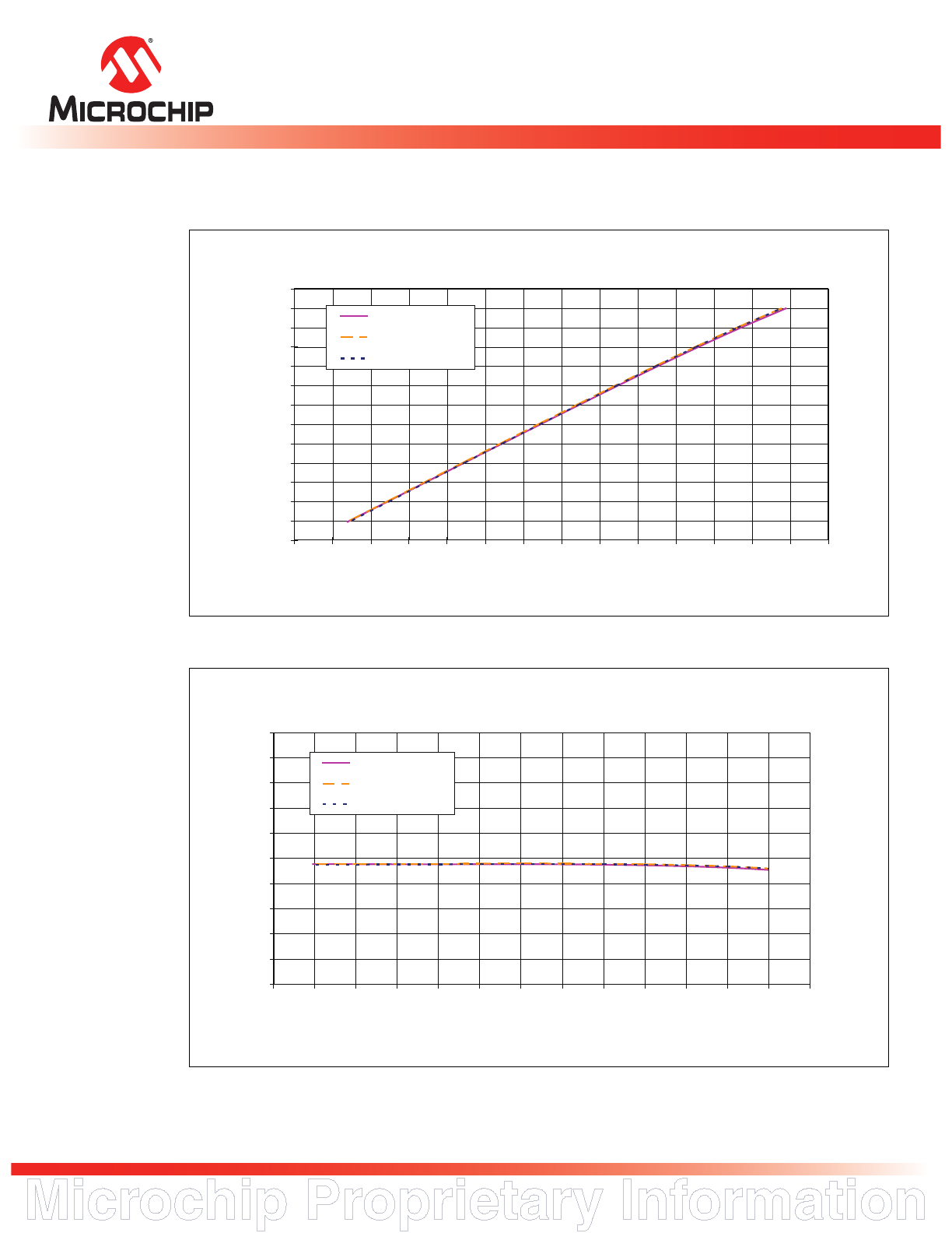
Figure 4: Low Band Output Power versus Input Power
Figure 5: Low Band Power Gain versus Output Power
Output Power versus Input Power
9
10
11
12
13
14
15
16
17
18
19
20
21
22
-21
-20
-19
-18
-17
-16
-15
-14
-13
-12
-11
-10
-9
-8
-7
Input Power (dBm)
Output Power (dBm)
Freq=2.412 GHz
Freq=2.442 GHz
Freq=2.484 GHz
1318 F5.1
Power Gain versus Output Power
20
22
24
26
28
30
32
34
36
38
40
9
10
11
12
13
14
15
16
17
18
19
20
21
22
Output Power (dBm)
Power Gain (dB)
Freq=2.412 GHz
Freq=2.442 GHz
Freq=2.484 GHz
1318 F6.1
Microchip Proprietary Information
©2012 Silicon Storage Technology, Inc.
DS75032A
10/12
9
2.4-2.5 GHz / 4.9-5.8 GHz Dual-Band Power Amplifier
SST13LP05
Data Sheet
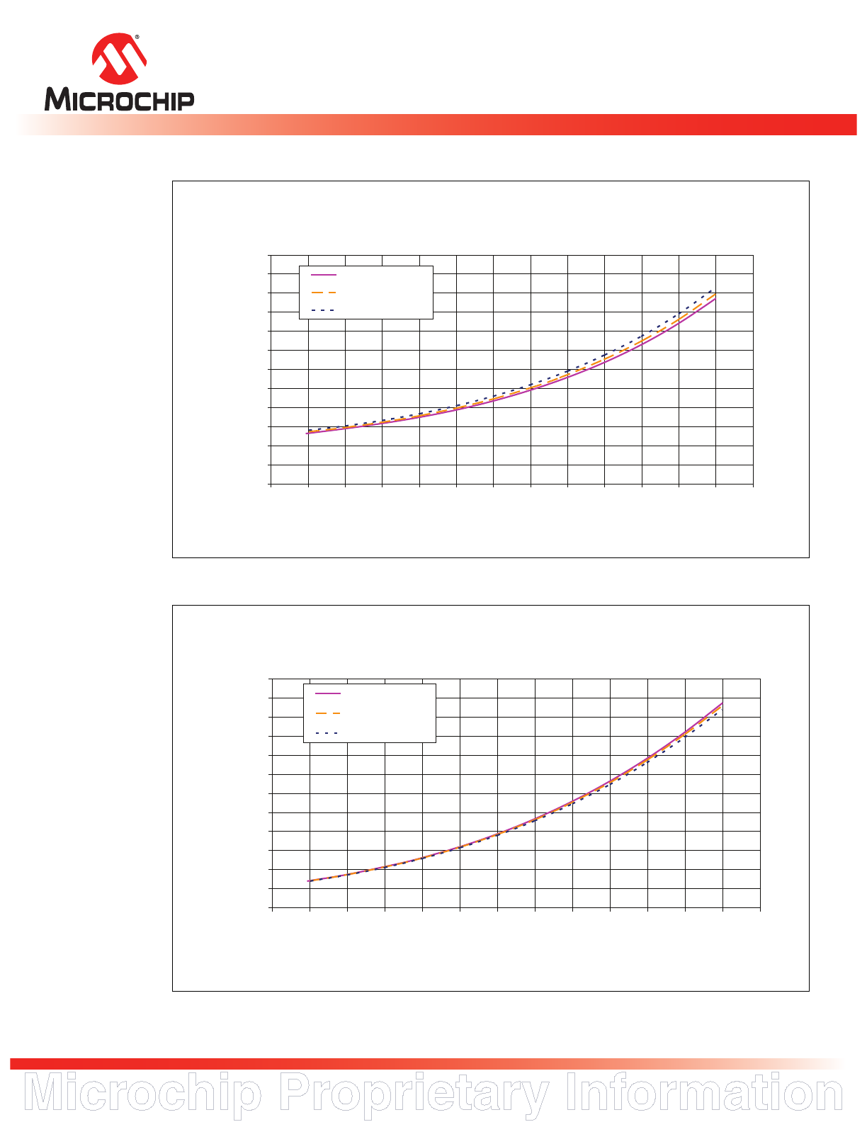
Figure 6: Low Band Supply Current versus Output Power
Figure 7: Low Band PAE versus Output Power
Supply Current versus Output Power
80
90
100
110
120
130
140
150
160
170
180
190
200
9
10
11
12
13
14
15
16
17
18
19
20
21
22
Output Power (dBm)
Supply Current (mA)
Freq=2.412 GHz
Freq=2.442 GHz
Freq=2.484 GHz
1318 F7.1
PAE versus Output Power
0
2
4
6
8
10
12
14
16
18
20
22
24
9
10
11
12
13
14
15
16
17
18
19
20
21
22
Output Power (dBm)
PAE (%)
Freq=2.412 GHz
Freq=2.442 GHz
Freq=2.484 GHz
1318 F8.1
Microchip Proprietary Information
©2012 Silicon Storage Technology, Inc.
DS75032A
10/12
10
2.4-2.5 GHz / 4.9-5.8 GHz Dual-Band Power Amplifier
SST13LP05
Data Sheet
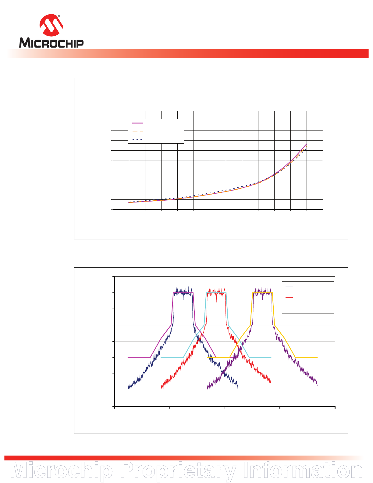
Figure 8: Low Band EMV versus Output Power, Measured with Sequence-plus-data
Equalizer Training
Figure 9: Low Band 802.11b Spectrum Mask at 23 dBm with DC Current of 220 mA
EVM versus Output Power
0
1
2
3
4
5
6
7
8
9
10
9
10
11
12
13
14
15
16
17
18
19
20
21
22
Output Power (dBm)
EVM (%)
Freq=2.412 GHz
Freq=2.442 GHz
Freq=2.484 GHz
1318 F9.1
-70
-60
-50
-40
-30
-20
-10
0
10
2.35
2.40
2.45
2.50
2.55
Frequency (GHz)
Amplitude (dB)
Freq = 2.412 GHz
Freq = 2.442 GHz
Freq = 2.484 GHz
1318 F11.0