

PR
OPRIET
AR
Y AND
CONFIDENTIAL
A Microchip Technology Company
©2011 Silicon Storage Technology, Inc.
DS75010B
09/11
Data Sheet
www.microchip.com
Features
• Input/output ports are matched to 50
internally
and DC decoupled.
• Packages available
– 20-contact UQFN – 3mm x 3mm x 0.55mm
• All non-Pb (lead-free) devices are RoHS compliant
Transmitter Chain:
• High gain:
– Typically 28 dB gain across 2.4–2.5 GHz over tempera-
ture -20°C to +85°C for Transmitter.
• High linear output power:
– Meets 802.11g OFDM ACPR requirement up to 21 dBm
– 3% added EVM up to 19 dBm for 54 Mbps 802.11g signal
– Meets 802.11b ACPR requirement up to 22 dBm
• High power-added efficiency/Low operating cur-
rent for 802.11b/g/n applications
– ~25% @ P
OUT
= 22 dBm for 802.11b/g
• Low I
REF
power-up/down control
– I
REF
<2 mA
• Low quiescent current
– ~55 mA I
CQ
• High-speed power-up/down
– Turn on/off time (10%- 90%) <100 ns
– Typical power-up/down delay with driver delay included
<200 ns
• Low shut-down current (~2 µA)
• Limited variation over temperature
– ~1 dB power variation between -20°C to +85°C
– ~2 dB gain variation between -20°C to +85°C
• Temperature and load insensitive on-chip power
detector
– >20 dB dynamic range, temperature-stable, on-chip
power detection
Receiver Chain:
• LNA ON:
– Typically 12 dB gain
– 3.1 dB noise figure
– >5dB P1dB
Bluetooth Path:
• Typically 2.5 dB loss
• Simultaneous BT/WLAN Rx mode:
– 8 dB gain
– 3.1 dB noise figure
Applications
• WLAN (IEEE 802.11b/g/n)
• Home RF
• Cordless phones
• 2.4 GHz ISM wireless equipment
• Zigbee®
• Bluetooth®
2.4 GHz High-Gain, High-Efficiency Front-end Module
SST12LF03
The SST12LF03 is a fully integrated Front-End Module (FEM) for WLAN 802.11b/g/
n and Bluetooth® systems. The SST12LF03 RF modules includes a PA, a LNA,
and an antenna switch, making it ideal for WLAN/BT embedded applications where
small size and high performance are required. Designed in compliance with IEEE
802.11 b/g/n applications and based on GaAs PHEMT/HBT technology, the
SST12LF03 operates within the frequency range of 2.4- 2.5 GHz with a very low
DC-current consumption. The Transmitter chain has excellent linearity, typically 3%
added EVM up to 19 dBm output power for 54 Mbps 802.11g operation, while meet-
ing 802.11b spectrum mask at 22 dBm. The receiver chain provides a low noise
amplifier and has options for simultaneous WLAN and Bluetooth operation.The
SST12LF03 is offered in a 20-contact UQFN package.

PR
OPRIET
AR
Y AND
CONFIDENTIAL
©2011 Silicon Storage Technology, Inc.
DS75010B
09/11
2
2.4 GHz High-Gain, High-Efficiency Front-end Module
SST12LF03
Data Sheet
A Microchip Technology Company
Product Description
The SST12LF03 is a 2.4 GHz Front-end Module (FEM) designed in compliance with IEEE 802.11b/g/n
applications. It combines a high-performance Power Amplifier (PA), a low-noise amplifier, and an
antenna switch. The single-pole, three-throw, antenna switch provides WLAN transmit and receive
capability as well as Bluetooth® connectivity. The receive path also allow for simultaneous WLAN and
Bluetooth operation.
The TX chain includes a high-efficiency PA based on the InGaP/GaAs HBT technology. This chain typ-
ically provides 28 dB gain with 25% power-added efficiency (PAE) @ POUT = 22 dBm for 802.11g and
802.11b operation.
The TX chain has excellent linearity, typically 3% added EVM at 19 dBm output power for 54 Mbps
802.11g operation, while meeting 802.11g spectrum mask at 22 dBm.
The SST12LF03 also features easy board-level usage along with high-speed power-up/down controls.
Ultra-low reference current (total I
REF
~2 mA) makes the SST12LF03 controllable directly from the
baseband chip. These features, coupled with low operating current, make the SST12LF03 ideal for the
final stage power amplification in battery-powered 802.11b/g/n WLAN transmitter applications.
The SST12LF03 transmitter has a linear on-chip, single-ended power detector, which is temperature
stable, load insensitive, and has a linear dynamic range greater than 20 dB. The excellent on-chip
power detector provides a reliable solution to board-level power control. In addition, the receiver path
includes an LNA, has the option for simultaneous WLAN and Bluetooth operation, and an optional low-
loss LNA bypass path. In WLAN operating mode, the receiver provides typically 12 dB gain and only
3.1 dB noise figure and >5 dB P1dB. Operating with simultaneous WLAN/BT, the receiver will provide
both the WLAN and Bluetooth ports with 8 dB gain and 3.1 dB noise figure.
All input/output RF ports are single-ended, DC blocked, and internally matched to 50
No external
DC-blocking capacitors or matching components are necessary. This helps reduce the system board
Bill of Materials (BOM) cost.
The SST12LF03 is offered in a 20-contact UQFN package. See Figure 2 for pin assignments and Table
1 for pin descriptions.
PR
OPRIET
AR
Y AND
CONFIDENTIAL
©2011 Silicon Storage Technology, Inc.
DS75010B
09/11
3
2.4 GHz High-Gain, High-Efficiency Front-end Module
SST12LF03
Data Sheet
A Microchip Technology Company
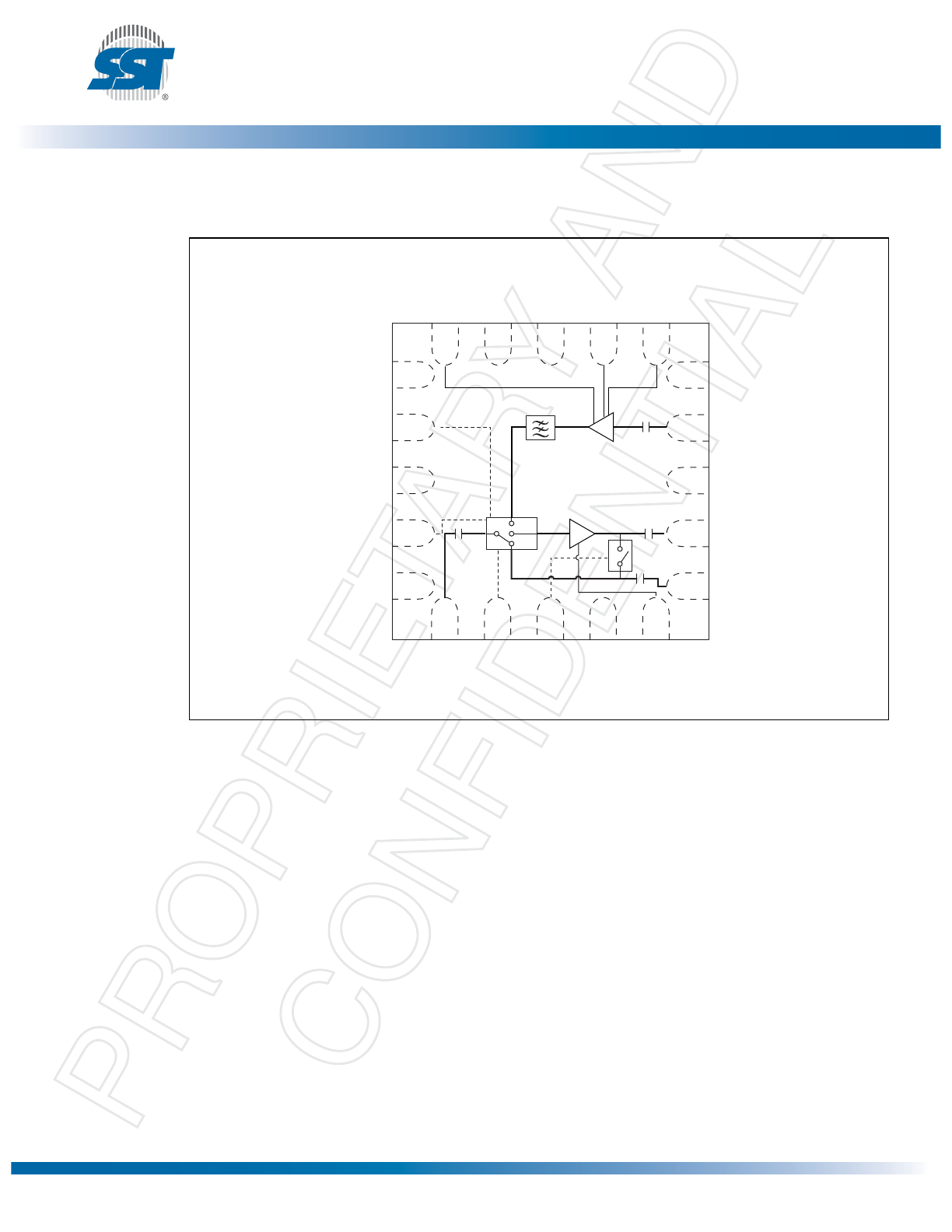
Functional Blocks
Figure 1: Functional Block Diagram
20
75010 B1.1
DNC
TX
GND
RX
BT
DNC
SRX
DNC
STX
SREF
VCC2
LEN
PEN
VCC1
DET
ANT
SBT
SBTR
CND
VCC3
19
18
17
16
6
7
8
9
10
11
12
13
14
15
5
4
3
2
1
PR
OPRIET
AR
Y AND
CONFIDENTIAL
©2011 Silicon Storage Technology, Inc.
DS75010B
09/11
4
2.4 GHz High-Gain, High-Efficiency Front-end Module
SST12LF03
Data Sheet
A Microchip Technology Company
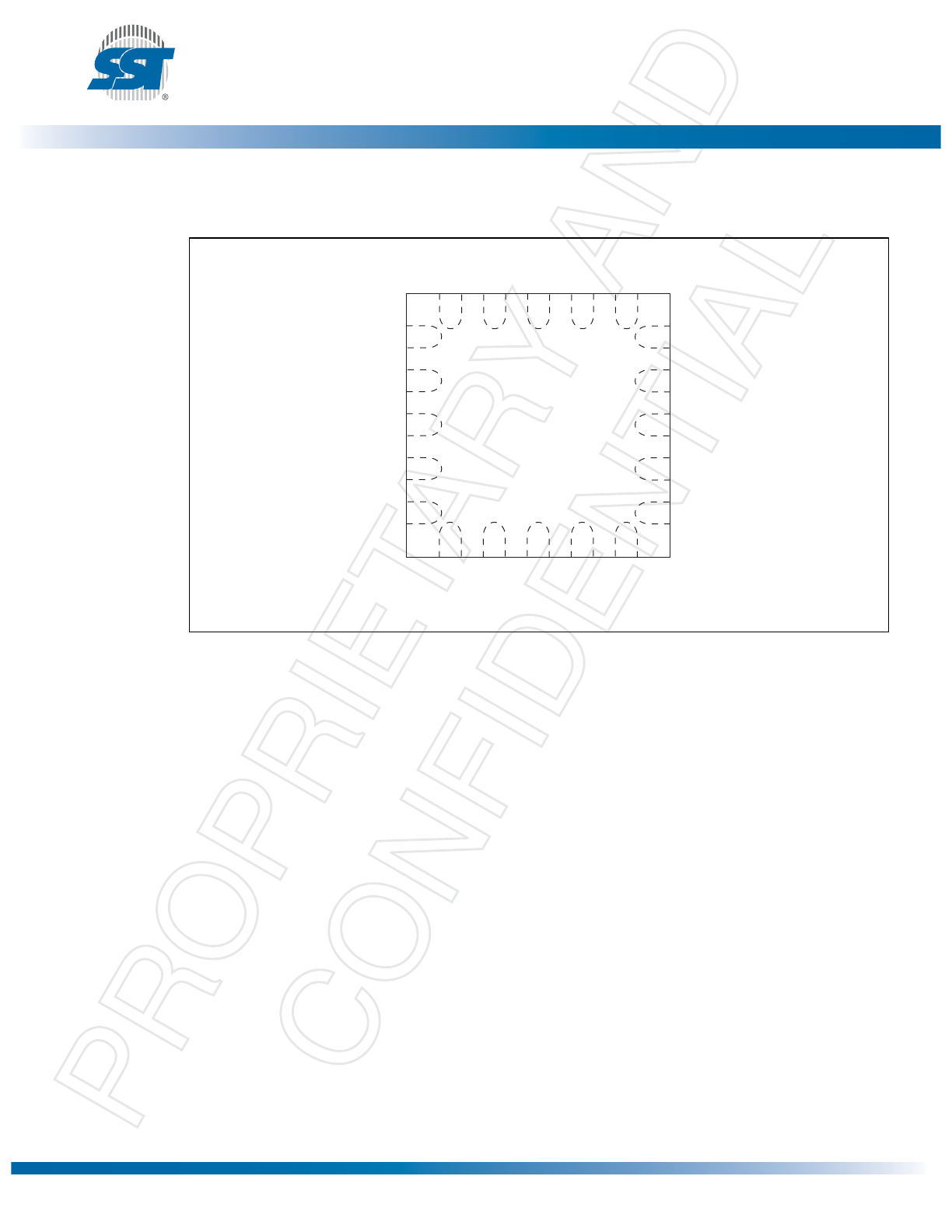
Pin Assignments
Figure 2: Pin Assignments for 20-contact UQFN
20
75010 P1.0
DNC
TX
GND
RX
BT
DNC
SRX
DNC
STX
SREF
VCC2
LEN
PEN
VCC1
DET
ANT
SBT
SBTR
CND
VCC3
19
18
17
16
6
7
8
9
10
11
12
13
14
15
5
4
3
2
1
3x3 UQFN
PR
OPRIET
AR
Y AND
CONFIDENTIAL
©2011 Silicon Storage Technology, Inc.
DS75010B
09/11
5
2.4 GHz High-Gain, High-Efficiency Front-end Module
SST12LF03
Data Sheet
A Microchip Technology Company
Pin Descriptions
Table 1: Pin Description
Symbol
Pin No.
Pin Name
Type
1
1. I=Input, O=Output
Function
DNC
1
Do Not Connect
Do not connect to this pin
SRX
2
WLAN Receive Antenna Switch control
DNC
3
Do Not Connect
Do not connect to this pin
STX
4
STX
WLAN Transmit Antenna Switch control
SREF
5
C
REF
Control pin reference high-level input
ANT
6
Antenna
I/O
Antenna port, AC coupled
SBT
7
SBT
BT antenna switch control
SBTR
8
SBTR
Switch control for simultaneous BT/RX
GND
9
Ground
Ground pin
VCC3
10
V
CC3
PWR
LNA power supply
BT
11
BT port, AC coupled
RX
12
R
X
I
WLAN receive port, AC coupled
GND
13
Ground
Ground pin
TX
14
T
X
O
WLAN transmit port, AC coupled
DNC
15
Do Not Connect
Do not connect to this pin
DET
16
WLAN transmit power detector
VCC1
17
V
CC1
WLAN power amplifier power supply #1
PEN
18
WLAN PA enable
LEN
19
LNA enable
VCC2
20
V
CC2
PWR
WLAN power amplifier power supply #2
Center
GND
Ground
Ground pin
T1.0 75010
PR
OPRIET
AR
Y AND
CONFIDENTIAL
©2011 Silicon Storage Technology, Inc.
DS75010B
09/11
6
2.4 GHz High-Gain, High-Efficiency Front-end Module
SST12LF03
Data Sheet
A Microchip Technology Company
Electrical Specifications
The DC and RF specifications for the power amplifier are specified below. Refer to Table 3 for the DC voltage
and current specifications. Refer to Figures 3 through 9 for the RF performance.
Absolute Maximum Stress Ratings (Applied conditions greater than those listed under “Absolute
Maximum Stress Ratings” may cause permanent damage to the device. This is a stress rating only and
functional operation of the device at these conditions or conditions greater than those defined in the
operational sections of this data sheet is not implied. Exposure to absolute maximum stress rating con-
ditions may affect device reliability.)
Input power to pin 3 (P
IN
). . . . . . . . . . . . . . . . . . . . . . . . . . . . . . . . . . . . . . . . . . . . . . . . . . . . . +5 dBm
Average output power from pin 11 (P
OUT
)
1
. . . . . . . . . . . . . . . . . . . . . . . . . . . . . . . . . . . . . . +26 dBm
1. Never measure with CW source. Pulsed single-tone source with <50% duty cycle is recommended. Exceeding the max-
imum rating of average output power could cause permanent damage to the device.
Supply Voltage at pins 6 and 9 (V
CC
) . . . . . . . . . . . . . . . . . . . . . . . . . . . . . . . . . . . . . . -0.3V to +4.2V
Reference voltage to pin 4 (V
REF
) . . . . . . . . . . . . . . . . . . . . . . . . . . . . . . . . . . . . . . . . . -0.3V to +3.3V
DC supply current (I
CC
)
2
. . . . . . . . . . . . . . . . . . . . . . . . . . . . . . . . . . . . . . . . . . . . . . . . . . . . . 400 mA
2. Measured with 100% duty cycle 54 Mbps 802.11g OFDM Signal
Operating Temperature (T
A
) . . . . . . . . . . . . . . . . . . . . . . . . . . . . . . . . . . . . . . . . . . . . -40ºC to +85ºC
Storage Temperature (T
STG
) . . . . . . . . . . . . . . . . . . . . . . . . . . . . . . . . . . . . . . . . . . . -40ºC to +120ºC
Maximum Junction Temperature (T
J
) . . . . . . . . . . . . . . . . . . . . . . . . . . . . . . . . . . . . . . . . . . . +150ºC
Surface Mount Solder Reflow Temperature . . . . . . . . . . . . . . . . . . . . . . . . . . . 260°C for 10 seconds
Table 2: Operating Range
Range
Ambient Temp
V
CC
Extended
-20°C to +85°C
3.3V
Table 3: DC Electrical Characteristics
Symbol
Parameter
Min.
Typ
Max.
Unit
V
CC
TX Supply Voltage at pins 6 and 9
3.0
3.3
4.2
V
I
CQ
TX Idle current for 802.11g to meet EVM ~3% @ 19 dBm
55
mA
V
REG
TX Reference Voltage
2.75
2.80
2.95
V
PEN
PA Enabled; PA Off
2.0
V
I
CC
TX Supply Current
for 11g OFDM 54 Mbps signal, P
OUT
= 22 dBm
175
mA
for 11b DSSS 1 Mbps signal, P
OUT
= 22 dBm
185
mA
V
DD
LNA Supply Voltage at pin 10
3.0
3.3
4.2
V
I
DD
LNA Supply Current
15
mA
V
CNTL
Control Voltage logic high, SRX, STX, SBT, LEN
2.8
3.3
V
CC
V
Control Voltage logic low
0
1.5
V
T3.1 75010
PR
OPRIET
AR
Y AND
CONFIDENTIAL
©2011 Silicon Storage Technology, Inc.
DS75010B
09/11
7
2.4 GHz High-Gain, High-Efficiency Front-end Module
SST12LF03
Data Sheet
A Microchip Technology Company
Table 4: TX Chain WLAN RF Characteristics
Symbol
Parameter
Min.
Typ
Max.
Unit
Test Condition
F
L-U
Frequency range
2412
2484
MHz
G
Small signal gain
26
29
dB
TX and PA On
G
VAR1
Gain variation over band (2412–2484 MHz)
±0.5
dB
TX and PA On
G
VAR2
Gain ripple over channel (20 MHz)
0.2
dB
TX and PA On
P
OUT
Output power meets 11g OFDM 6 Mbps spectrum
mask
20
22
dBm
TX and PA On
Output power meets 11b DSSS 1 Mbps spectrum
mask
20
22
dBm
TX and PA On
Added
EVM
@ 19 dBm output power with 11g OFDM 54 Mbps
signal
3
%
TX and PA On
2f, 3f, 4f, 5f Harmonics at 22 dBm, without external filters
-35
dBc
TX and PA On
ISO1
Isolation (TX to RX)
-12
dB
TX and PA On
ISO2
Isolation (TX to BT)
-10
dB
TX and PA On
ISO3
Isolation (RX to TX)
-30
dB
TX and PA On
ISO4
Isolation (BT to TX)
-50
dB
TX and PA On
T4.0 75010
Table 5: RX Chain WLAN RF Characteristics
Symbol
Parameter
Min.
Typ
Max.
Unit
Test Condition
F
L-U
Frequency range
2412
2484
MHz
G
ON
Gain with LNA on
10
12
dB
LEN=SRX=High
PEN=STX=SBT=SBTR=Low
P1dB
Receiver 1 dB compression
5
dBm
LEN=SRX=High
PEN=STX=SBT=SBTR=Low
G
ONS
Gain with LNA on and simultaneous
BT
7
8
dB
LEN=SRX=High
PEN=STX=SBT=Low
IL
S
Insertion loss with LNA bypassed to
BT and RX simultaneous
4.8
dB
SBT=SBTR=High
PEN=STX=SRX=LEN=Low
NF
ON
Noise figure with LNA on
3.1
dB
LEN=SRX=High
PEN=STX=SBT=SBTR=Low
NF
ONS
Noise figure with LNA on and simul-
taneous BT
3.1
dB
LEN=SRX=High
PEN=STX=SBT=Low
I
DD
Receiver supply current with LNA on
15
mA
LEN=High
ISO
BT-RX
Isolation BT to RX
17
dB
LEN=SRX=High
PEN=STX=SBT=SBTR=Low
ISO
BT-TX
Isolation TX to RX with TX on
25
dB
LEN=SRX=High
PEN=STX=SBT=SBTR=Low
RL
ANT
Receiver input return loss at the
antenna with LNA on
12
dB
LEN=SRX=High
PEN=STX=SBT=SBTR=Low
RL
RX
Receiver output return loss with
WLAN only
12
dB
LEN=SRX=High
PEN=STX=SBT=SBTR=Low
RX
RXS
Receiver output return loss with
simultaneous WLAN/BT
10
dB
LEN=SRX=High
PEN=STX=SBT=Low
T5.0 75010
PR
OPRIET
AR
Y AND
CONFIDENTIAL
©2011 Silicon Storage Technology, Inc.
DS75010B
09/11
8
2.4 GHz High-Gain, High-Efficiency Front-end Module
SST12LF03
Data Sheet
A Microchip Technology Company
Table 6: Bluetooth Chain RF Characteristics
Symbol
Parameter
Min.
Typ
Max.
Unit
Test Condition
F
L-U
Frequency range
2412
2484
MHz
IL
Loss: antenna to BT
2.5
dB
SBT=High
LEN=PEN=STX=SRX=SBTR=
Low
G
ONS
Gain with LNA on and simultaneous
BT
7
8
dB
LEN=SRX=SBTR=High
PEN=STX=SBT=Low
NF
ONS
Noise figure with LNA on and simul-
taneous BT
3.1
dB
LEN=SRX=SBTR=High
PEN=STX=SBT=Low
RL
ANT
Receiver input return loss at the
antenna with LNA on
12
dB
SBT=High
PEN=STX=SBTR=LEN=SRX=
Low
BT
RX
Receiver output return loss
12
dB
SBT=High
PEN=STX=SBTR=LEN=SRX=
Low
RX
RXS
Receiver output return loss with
simultaneous WLAN/BT
8
dB
SBT=SBTR=High
PEN=STX=LEN=SRX=Low
T6.0 75010
Table 7: Switch Control Logic
Mode
STX
SRX
SBT
SBTR
PEN
LEN
All Off (not supported)
L
L
L
L
L
L
Bluetooth On
L
L
H
L
L
H
WLAN TX On
H
L
L
L
H
L
WLAN RX On
L
H
L
L
L
H
Simultaneous WLAN/BT RX On
L
H
L
H
L
H
T7.0 75010
PR
OPRIET
AR
Y AND
CONFIDENTIAL
©2011 Silicon Storage Technology, Inc.
DS75010B
09/11
9
2.4 GHz High-Gain, High-Efficiency Front-end Module
SST12LF03
Data Sheet
A Microchip Technology Company
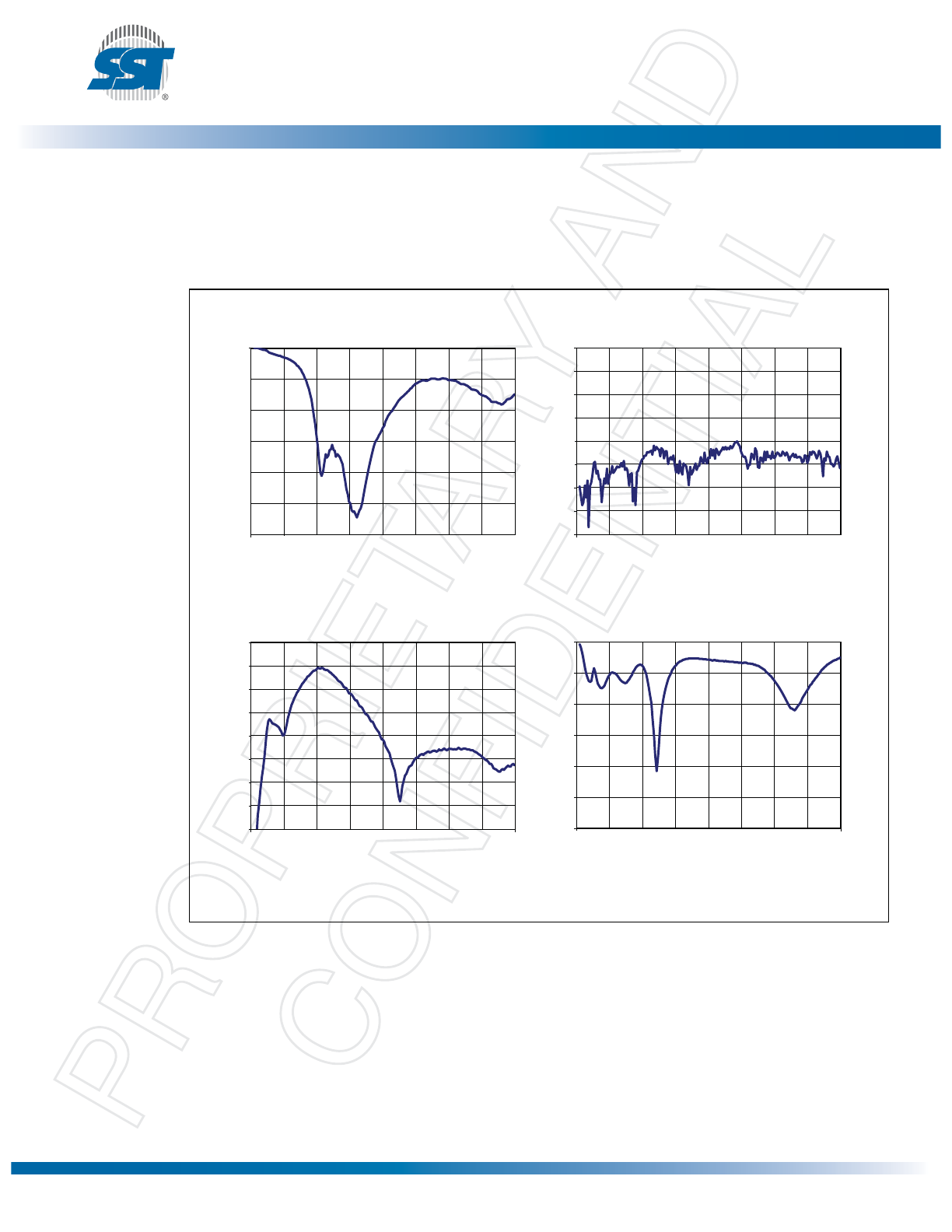
Typical WLAN Transmitter Performance Characteristics
Test Conditions: V
CC
= 3.3V, PEN=2.80V, STX=High, SRX=SBT=SBTR=Low,
T
A
= 25°C, unless otherwise specified
Figure 3: S-Parameters for WLAN Transmitter
S11 versus Frequency
-30
-25
-20
-15
-10
-5
0
0.0
1.0
2.0
3.0
4.0
5.0
6.0
7.0
Frequency (GHz)
S11
(dB)
Frequency (GHz)
S21
(dB)
S22
(dB)
Frequency (GHz)
S12
(dB)
Frequency (GHz)
75010 S-Parms.1.0
S12 versus Frequency
-80
-70
-60
-50
-40
-30
-20
-10
0
S21 versus Frequency
-40
-30
-20
-10
0
10
20
30
40
S22 versus Frequency
-30
-25
-20
-15
-10
-5
0
8.0
0.0
1.0
2.0
3.0
4.0
5.0
6.0
7.0
8.0
0.0
1.0
2.0
3.0
4.0
5.0
6.0
7.0
8.0
0.0
1.0
2.0
3.0
4.0
5.0
6.0
7.0
8.0
PR
OPRIET
AR
Y AND
CONFIDENTIAL
©2011 Silicon Storage Technology, Inc.
DS75010B
09/11
10
2.4 GHz High-Gain, High-Efficiency Front-end Module
SST12LF03
Data Sheet
A Microchip Technology Company
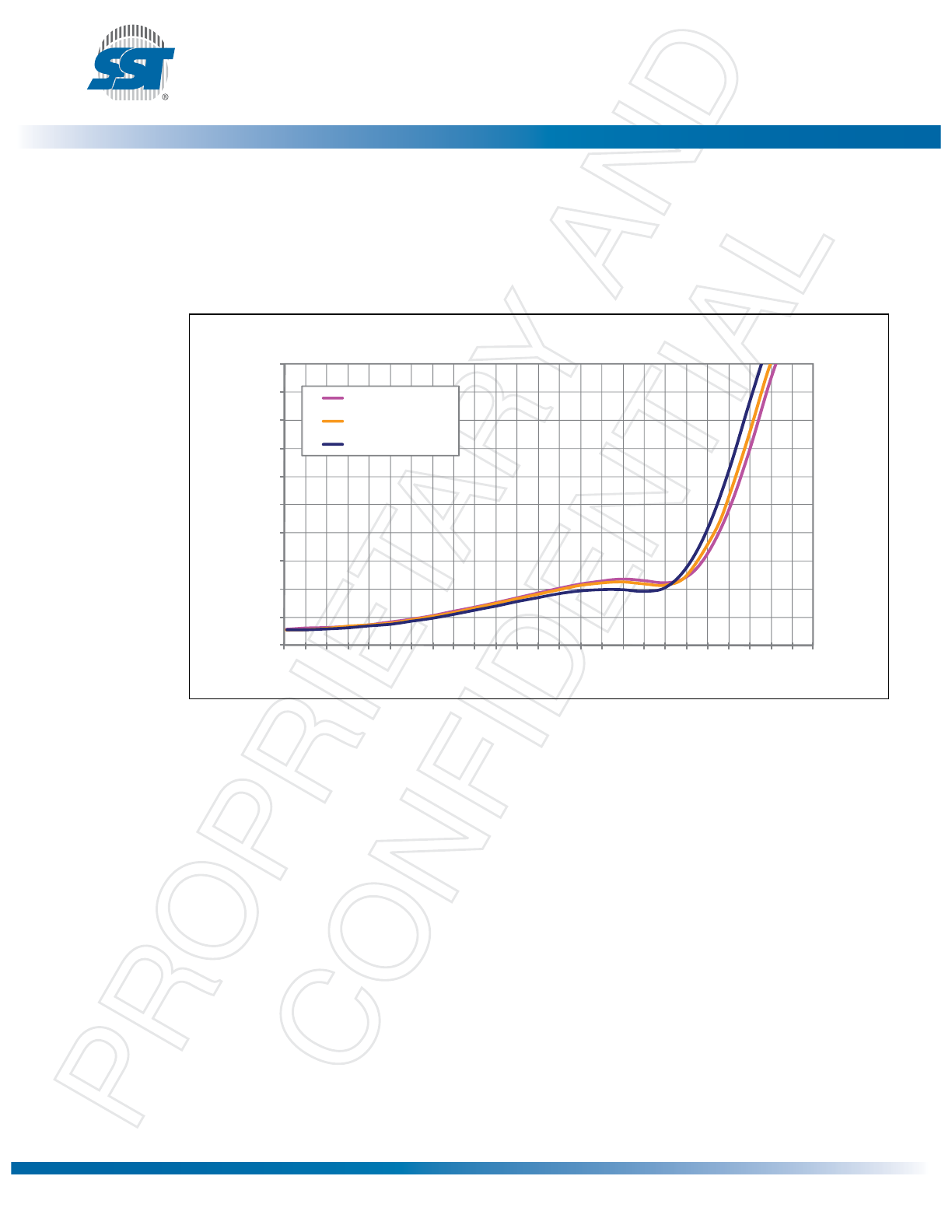
Typical WLAN Transmitter Performance Characteristics
Test Conditions: V
CC
= 3.3V, PEN=2.80V, STX=High, SRX=SBT=SBT=Low,
T
A
= 25°C, 54 Mbps 802.11g OFDM Signal
Equalizer Training Setting using Channel Estimation Sequence and Data
Figure 4: WLAN Tx EVM with 802.11g OFDM 54 Mbps
0
1
2
3
4
5
6
7
8
9
10
0
1
2
3
4
5
6
7
8
9 10 11 12 13 14 15 16 17 18 19 20 21 22 23 24 25
EVM (%)
Output Power (dBm)
EVM versus Output Power
Freq=2.412 GHz
Freq=2.442 GHz
Freq=2.472 GHz