
2017 Microchip Technology Inc.
DS20005900A-page 1
MIC44F18/19/20
Features
• 4.5V to 12.6V Input Operating Range
• 6A Peak Output Current
• High Accuracy ±5% Enable Input Threshold
• High Speed Switching Capability
- 10 ns Rise Time in 1000 pF Load
- <15 ns Propagation Delay Time
• Flexible UVLO Function
- 4.2V Internally Set UVLO
- Programmable with External Resistors
• Latch-Up Protection to >500 mA Reverse Current
on the Output Pin
• Enable Function
• Thermally Enhanced ePAD MSOP-8 Package
Option
• Miniature 2 mm x 2 mm DFN-8 Package Option
• Pb-Free Packaging
Applications
• Synchronous Switch-Mode Power Supplies
• Secondary Side Synchronous Rectification
General Description
The MIC44F18, MIC44F19, and MIC44F20 are
high-speed single MOSFET drivers capable of sinking
and sourcing 6A for driving capacitive loads. With delay
times of less than 15 ns and rise times into a 1000 pF
load of 10 ns, these MOSFET drivers are ideal for
driving large gate charge MOSFETs in power supply
applications. The MIC44F18 is a non-inverting driver,
the MIC44F19 is an inverting driver suited for driving
P-Channel MOSFETs, and the MIC44F20 is an
inverting driver for N-Channel MOSFETs.
Fabricated using proprietary BiCMOS/DMOS process
for low power consumption and high efficiency, the
MIC44F18/19/20 translates TTL or CMOS input logic
levels to output voltage levels that swing within 25 mV
of the positive supply or ground. Comparable bipolar
devices are capable of swinging only to within 1V of the
supply.
The input supply voltage range of the MIC44F18/19/20
is 4.5V to 12.6V, making the devices suitable for driving
MOSFETs in a wide range of power applications. Other
features include an enable function, latch-up
protection, and a programmable UVLO function.
The MIC44F18/19/20 has a junction temperature range
of –40°C to +125°C with exposed pad ePAD MSOP-8
and 2 mm x 2 mm DFN-8 package options.
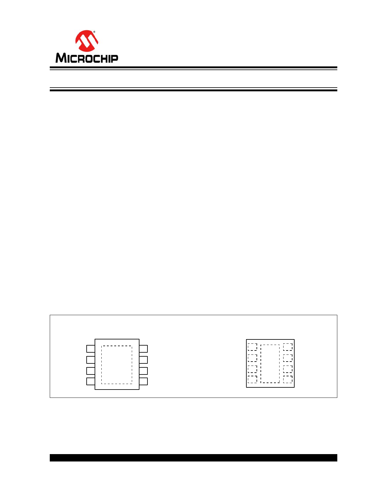
Package Types
Please see pin descriptions in
Table 3-1
.
IN
EN/UVLO
5
4
OUT
VDD
NC
OUT
GND
GND
8
7
6
1
2
3
EP
8-Pin ePAD MSOP
(MME)
IN
EN/UVLO
4
OUT
VDD
NC
OUT
GND
GND
8
7
6
1
2
3
5
EP
8-Pin 2 mm x 2 mm DFN
(ML)
6A, 12.6V High Speed MOSFET Drivers with Enable Input
MIC44F18/19/20
DS20005900A-page 2
2017 Microchip Technology Inc.
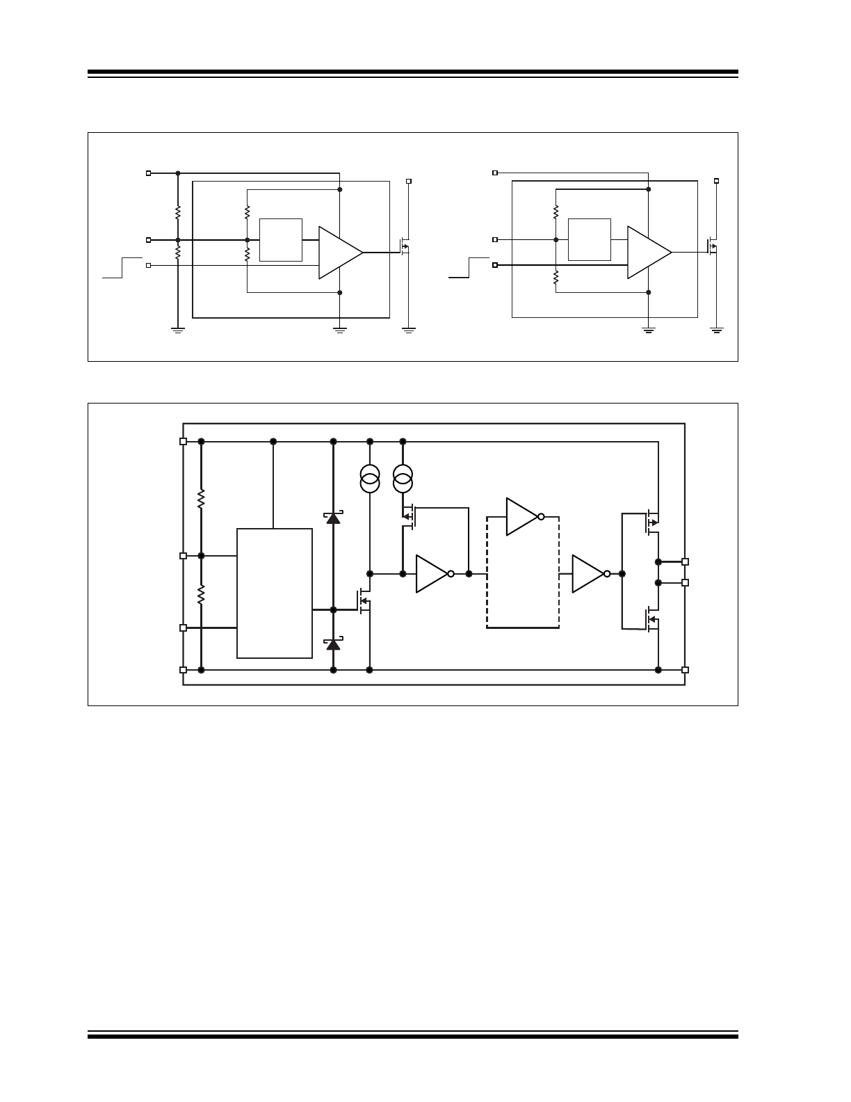
Typical Application Circuits
Functional Block Diagram
Input
600
Nȍ
240
Nȍ
VDD
EN/
UVLO
MIC44F18
IN
OUT
GND
4.5V to
12.6V
DRIV ER
40
Nȍ
10
Nȍ
EN/UVLO
DRIVER
MOSFET Driver with 6.2V UVLO Externally Set
Input
600
Nȍ
240
Nȍ
VDD
EN/
UVLO
MIC44F18
IN
OUT
GND
4.5V to
12.6V
DRIV ER
EN/UVLO
DRIVER
MOSFET Driver with 4.2V UVLO Internally Set
MIC4419/20:
Inverting
MIC4418:
Non-Inverting
OUT
VDD
EN/UVLO
VIN
(Control Input)
Nȍ
Nȍ
GND
EN/UVLO
and
Control
Input
OUT
GND

2017 Microchip Technology Inc.
DS20005900A-page 3
MIC44F18/19/20
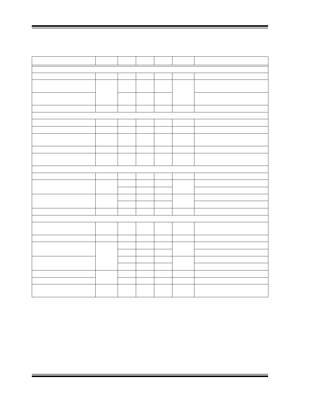
1.0
ELECTRICAL CHARACTERISTICS
Absolute Maximum Ratings †
Supply Voltage (V
DD
) ................................................................................................................................................+13V
UVLO/Enable Voltage (V
UVLO/EN
).............................................................................................................................+13V
Input Voltage (V
IN
) .................................................................................................................. (V
S
+ 0.1V) to (GND – 5V)
Output Voltage (V
OUT
) ..............................................................................................................................................+13V
ESD Rating (
Note 1
)
Pins 1, 2, 3, 5, 6, 7, 8 ................................................................................................................................................. 2 kV
Pin 4..........................................................................................................................................................................500V
Operating Ratings ‡
Supply Voltage (V
DD
) .............................................................................................................................. +4.5V to +12.6V
†
Notice: Stresses above those listed under “Absolute Maximum Ratings” may cause permanent damage to the device.
This is a stress rating only and functional operation of the device at those or any other conditions above those indicated
in the operational sections of this specification is not intended. Exposure to maximum rating conditions for extended
periods may affect device reliability.
‡ Notice:
The device is not guaranteed to function outside its operating ratings.
Note 1:
Devices are ESD sensitive. Handling precautions are recommended. Human body model, 1.5 kΩ in series
with 100 pF.
MIC44F18/19/20
DS20005900A-page 4
2017 Microchip Technology Inc.
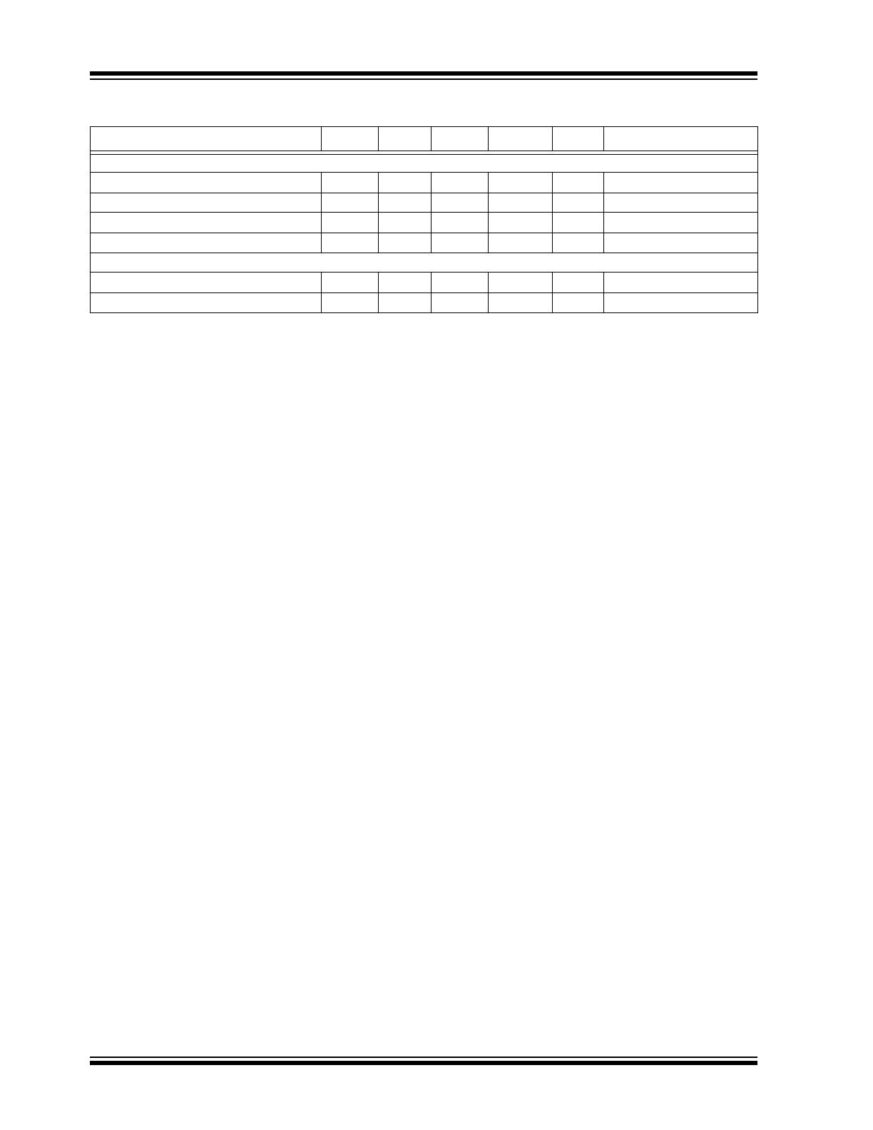
TABLE 1-1:
ELECTRICAL CHARACTERISTICS
Electrical Characteristics:
4.5V ≤ V
DD
≤ 12.6V, C
L
= 1000 pF; T
A
= +25°C.
Bold
values indicate –40°C ≤ T
J
≤ +125°C.
Note 1
Parameter
Symbol
Min.
Typ.
Max.
Units
Conditions
Power Supply
Supply Voltage Range
V
DD
4.5
—
12.6
V
—
High Output Quiescent
Current
I
S
—
—
2.5
mA
V
IN
= 5V (MIC44F18),
V
IN
= 0V (MIC44F19/20)
Low Output Quiescent
Current
—
—
2.5
V
IN
= 0V (MIC44F18),
V
IN
= 5V (MIC44F19/20)
Shutdown Current
I
SD
—
—
200
µA
V
EN
= 0V
EN/UVLO
Enable Threshold
V
EN
1.3
1.4
1.5
V
—
Enable Hysteresis
V
EN_HYS
—
120
—
mV
—
Undervoltage Lockout
Threshold (Internally Set)
V
UVLO
3.6
4.2
4.4
V
V
EN
= open, V
DD
rising.
UVLO Hysteresis
—
—
370
—
mV
—
Undervoltage Lockout
Threshold (Externally Set)
V
UVLO
V
EN(MAX)
—
V
DD
V
V
DD
rising
Input
Input Voltage Range
V
IN
0
—
V
DD
V
Steady State Voltage,
Note 2
Logic 1 Input Voltage
V
IH
1.615
1.7
1.785
V
T
A
= +25°C (±5%)
1.53
1.7
1.87
Over temperature range (±10%)
Logic 0 Input Voltage
V
IL
1.45
1.53
1.607
V
T
A
= +25°C (±5%)
1.377
1.53
1.683
Over temperature range (±10%)
Input Current
I
IN
—
—
5
µA
4.5V ≤ V
IN
≤ 10V
Output
Output High Voltage
V
OH
V
S
–
0.025
—
—
V
See
Functional Block Diagram
Output Low Voltage
V
OL
—
—
0.025
V
See
Functional Block Diagram
Output Resistance, Output
High
R
O
—
—
2
Ω
I
OUT
= 100 mA, V
DD
= 12V
—
—
3
I
OUT
= 100 mA, V
DD
= 5V
Output Resistance, Output
Low
—
—
2
Ω
I
OUT
= 100 mA, V
DD
= 12V
—
—
3
I
OUT
= 100 mA, V
DD
= 5V
Peak Output Sink Current
I
PEAK
6
—
—
A
V
DD
= 12V
Peak Output Source Current
6
—
—
A
V
S
= 12V
Latch-Up Protection
Withstand Reverse Current
I
R
>500
—
—
mA
—
2017 Microchip Technology Inc.
DS20005900A-page 5
MIC44F18/19/20
Switching Time
Rise Time
t
R
—
10
20
ns
V
S
= 12V, C
L
= 1000 pF
See Timing Diagram
Fall Time
t
F
—
10
20
ns
V
S
= 12V, C
L
= 1000 pF
See Timing Diagram
Delay Time
t
D1
—
15
35
ns
V
S
= 12V, C
L
= 1000 pF
See Timing Diagram
Delay Time
t
D2
—
13
35
ns
V
S
= 12V, C
L
= 1000 pF
See Timing Diagram
Pulse Width
t
PW
50
—
—
ns
V
S
= 12V, See Timing Diagram
Maximum Input Frequency
f
MAX
—
Note 3
—
MHz
V
S
= 12V, See Timing Diagram 2
Note 1:
Specification for packaged product only
2:
The device is protected from damage when –5V< V
IN
< 0V. However, 0V is the recommended minimum
continuous V
IL
voltage. See the Application Information section for additional information.
3:
See Application Information section for information on the maximum operating frequency.
TABLE 1-1:
ELECTRICAL CHARACTERISTICS (CONTINUED)
Electrical Characteristics:
4.5V ≤ V
DD
≤ 12.6V, C
L
= 1000 pF; T
A
= +25°C.
Bold
values indicate –40°C ≤ T
J
≤ +125°C.
Note 1
Parameter
Symbol
Min.
Typ.
Max.
Units
Conditions
MIC44F18/19/20
DS20005900A-page 6
2017 Microchip Technology Inc.
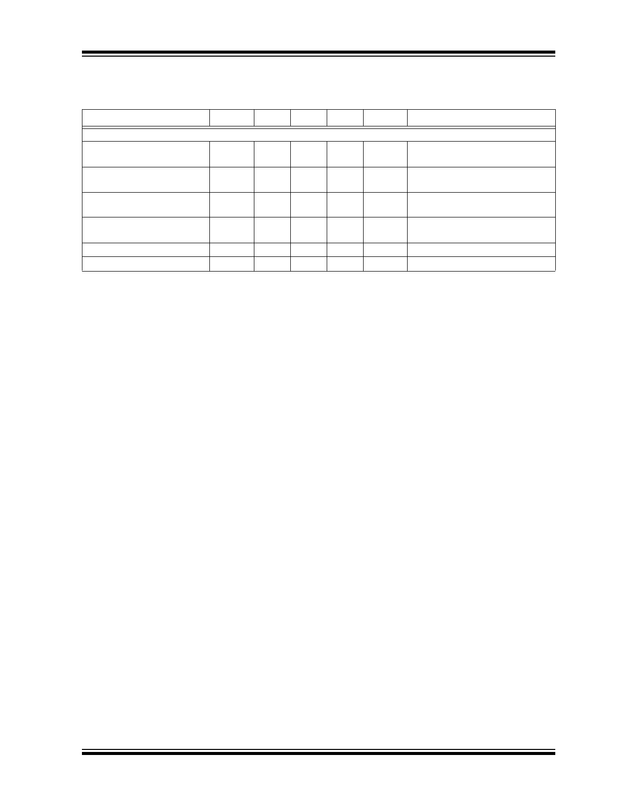
TEMPERATURE SPECIFICATIONS (
Note 1
)
Parameters
Sym.
Min.
Typ.
Max.
Units
Conditions
Temperature Ranges
Operating Junction Temperature
T
J
—
—
+125
°C
—
Maximum Junction Temperature
—
—
—
+150
°C
—
Storage Temperature Range
T
DD
–65
—
+150
°C
—
Lead Temperature
—
—
—
+300
°C
Soldering, 10s
Package Thermal Resistances
Thermal Resistance ePAD MSOP-8
JA
—
78
—
°C/W
—
Thermal Resistance 3x3 DFN-8Ld
JA
—
93
—
°C/W
—
Note 1:
The maximum allowable power dissipation is a function of ambient temperature, the maximum allowable
junction temperature and the thermal resistance from junction to air (i.e., T
A
, T
J
,
JA
). Exceeding the
maximum allowable power dissipation will cause the device operating junction temperature to exceed the
maximum +125°C rating. Sustained junction temperatures above +125°C can impact the device reliability.
2017 Microchip Technology Inc.
DS20005900A-page 7
MIC44F18/19/20
2.0
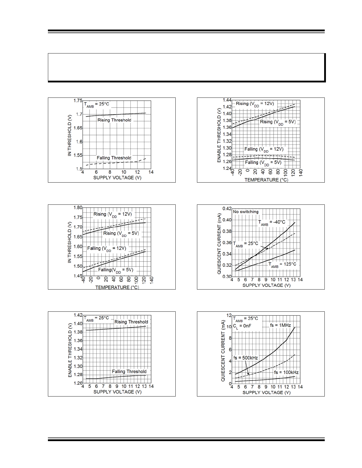
TYPICAL PERFORMANCE CURVES
FIGURE 2-1:
IN Threshold vs. Supply
Voltage.
FIGURE 2-2:
IN Threshold vs.
Temperature.
FIGURE 2-3:
Enable Threshold vs.
Supply Voltage.
FIGURE 2-4:
Enable Threshold vs.
Temperature.
FIGURE 2-5:
Quiescent Current vs.
Supply Voltage.
FIGURE 2-6:
Quiescent Current vs.
Supply Voltage.
Note:
The graphs and tables provided following this note are a statistical summary based on a limited number of
samples and are provided for informational purposes only. The performance characteristics listed herein
are not tested or guaranteed. In some graphs or tables, the data presented may be outside the specified
operating range (e.g., outside specified power supply range) and therefore outside the warranted range.
MIC44F18/19/20
DS20005900A-page 8
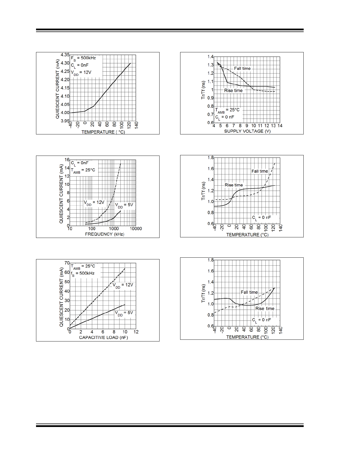
2017 Microchip Technology Inc.
FIGURE 2-7:
Quiescent Current vs.
Temperature.
FIGURE 2-8:
Quiescent Current vs.
Frequency.
FIGURE 2-9:
Quiescent Current vs.
Capacitive Load.
FIGURE 2-10:
Rise and Fall Time vs.
Supply Voltage.
FIGURE 2-11:
Rise and Fall Time (5V) vs.
Temperature.
FIGURE 2-12:
Rise and Fall Time (12V) vs.
Temperature.
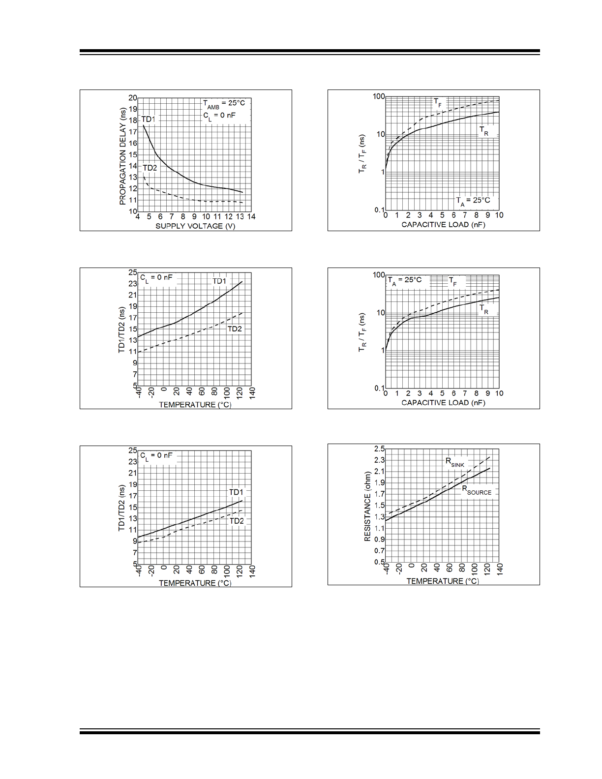
2017 Microchip Technology Inc.
DS20005900A-page 9
MIC44F18/19/20
FIGURE 2-13:
Propagation Delay vs.
Supply Voltage.
FIGURE 2-14:
Propagation Delay (5V) vs.
Temperature.
FIGURE 2-15:
Propagation Delay (12V) vs.
Temperature.
FIGURE 2-16:
Rise and Fall Time (5V) vs.
Capacitive Load.
FIGURE 2-17:
Rise and Fall Time (12V) vs.
Capacitive Load.
FIGURE 2-18:
Output Impedance (5V) vs.
Temperature.
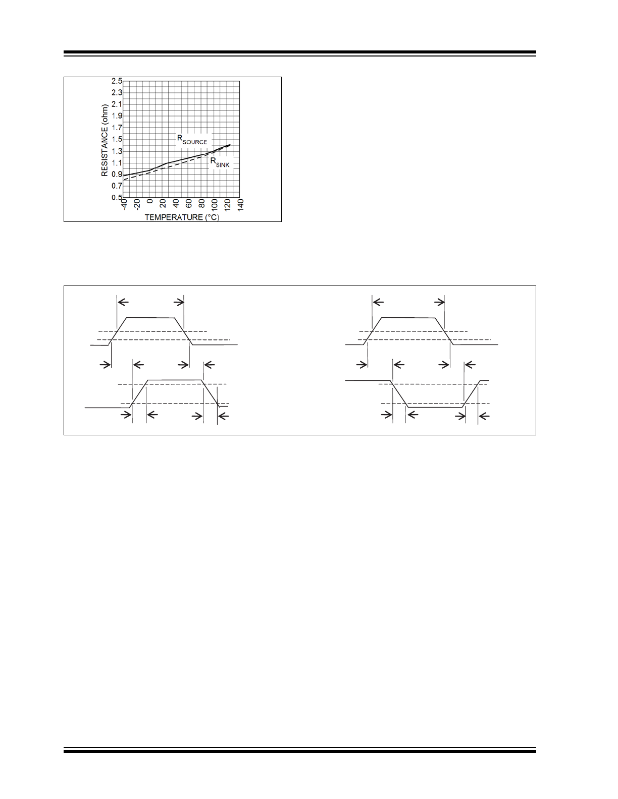
MIC44F18/19/20
DS20005900A-page 10
2017 Microchip Technology Inc.
FIGURE 2-19:
Output Impedance (12V) vs.
Temperature
.
Timing Diagram
D2
t
D1
50%
threshold
t
F
t
R
Out
V
IN
90%
10%
t
PW
t
D2
t
D1
50%
V
IN
threshold
t
F
t
R
90%
10%
t
PW
Out
V
IN
V
IN
t