
1998-2013 Microchip Technology Inc.
DS40182D-page 1
Devices included in this data sheet:
• PIC16CE623
• PIC16CE624
• PIC16CE625
High Performance RISC CPU:
• Only 35 instructions to learn
• All single-cycle instructions (200 ns), except for
program branches which are two-cycle
• Operating speed:
- DC - 20 MHz clock input
- DC - 200 ns instruction cycle
• Interrupt capability
• 16 special function hardware registers
• 8-level deep hardware stack
• Direct, Indirect and Relative addressing modes
Peripheral Features:
• 13 I/O pins with individual direction control
• High current sink/source for direct LED drive
• Analog comparator module with:
- Two analog comparators
- Programmable on-chip voltage reference
(V
REF
) module
- Programmable input multiplexing from device
inputs and internal voltage reference
- Comparator outputs can be output signals
• Timer0: 8-bit timer/counter with 8-bit
programmable prescaler
Special Microcontroller Features:
• In-Circuit Serial Programming (ICSP™) (via two
pins)
• Power-on Reset (POR)
• Power-up Timer (PWRT) and Oscillator Start-up
Timer (OST)
• Brown-out Reset
• Watchdog Timer (WDT) with its own on-chip RC
oscillator for reliable operation
Device
Program
Memory
RAM
Data
Memory
EEPROM
Data
Memory
PIC16CE623
512x14
96x8
128x8
PIC16CE624
1Kx14
96x8
128x8
PIC16CE625
2Kx14
128x8
128x8
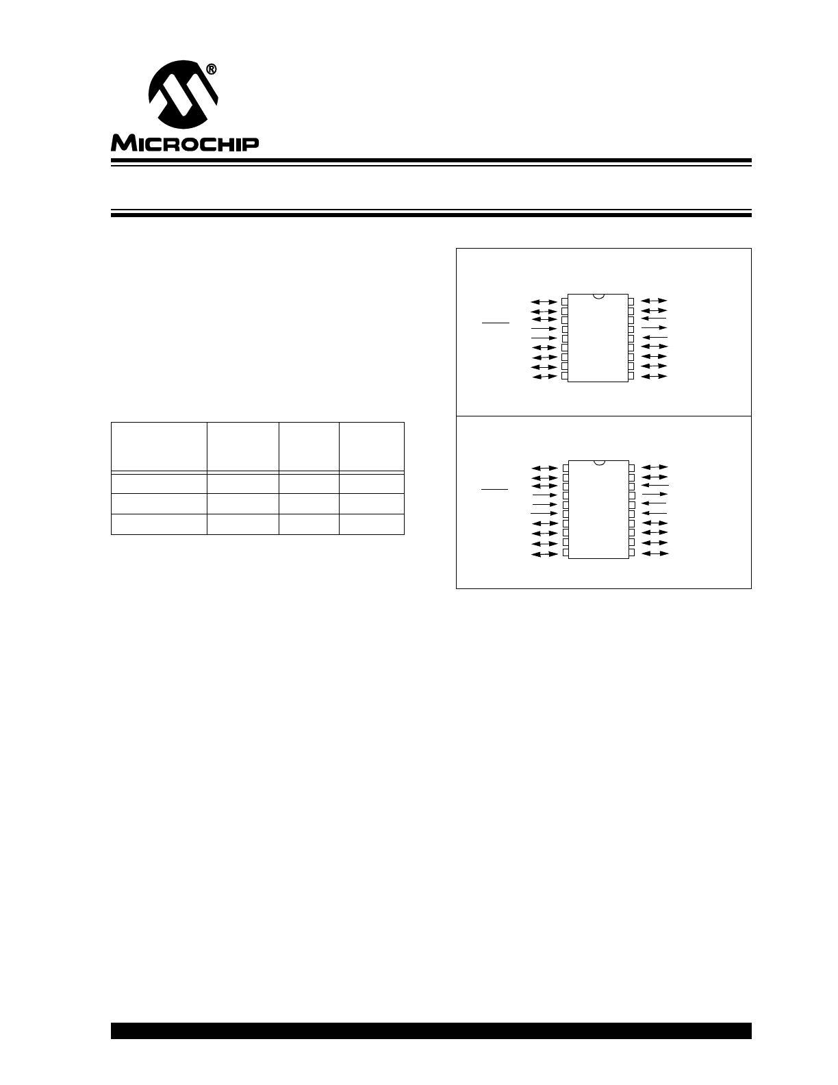
Pin Diagrams
Special Microcontroller Features (cont’d)
• 1,000,000 erase/write cycle EEPROM data
memory
• EEPROM data retention > 40 years
• Programmable code protection
• Power saving SLEEP mode
• Selectable oscillator options
• Four user programmable ID locations
CMOS Technology:
• Low-power, high-speed CMOS EPROM/EEPROM
technology
• Fully static design
• Wide operating voltage range
- 2.5V to 5.5V
• Commercial, industrial and extended temperature
range
• Low power consumption
- < 2.0 mA @ 5.0V, 4.0 MHz
- 15
A typical @ 3.0V, 32 kHz
- < 1.0
A typical standby current @ 3.0V
RA1/AN1
RA0/AN0
OSC2/CLKOUT
V
DD
RB7
RB6
RB5
RB4
OSC1/CLKIN
RA2/AN2/V
REF
RA3/AN3
MCLR/V
PP
V
SS
RB0/INT
RB1
RB2
RB3
RA4/T0CKI
PI
C
16C
E6
2X
RA1/AN1
RA0/AN0
OSC2/CLKOUT
V
DD
RB7
RB6
RB5
RB4
OSC1/CLKIN
RA2/AN2/V
REF
RA3/AN3
MCLR/V
PP
V
SS
V
SS
RB0/INT
RB1
RB2
RA4/T0CKI
PIC1
6CE62
X
RB3
RB3
V
DD
PDIP, SOIC, Windowed CERDIP
SSOP
2
3
4
5
6
7
8
9
10
•1
2
3
4
5
6
7
8
9
•1
19
18
16
15
14
13
12
11
17
18
17
15
14
13
12
11
10
16
20
OTP 8-Bit CMOS MCU with EEPROM Data Memory
PIC16CE62X

PIC16CE62X
DS40182D-page 2
1998-2013 Microchip Technology Inc.
Table of Contents
1.0
General Description ............................................................................................................................................... 3
2.0
PIC16CE62X Device Varieties .............................................................................................................................. 5
3.0
Architectural Overview........................................................................................................................................... 7
4.0
Memory Organization .......................................................................................................................................... 11
5.0
I/O Ports............................................................................................................................................................... 23
6.0
EEPROM Peripheral Operation ........................................................................................................................... 29
7.0
Timer0 Module..................................................................................................................................................... 35
8.0
Comparator Module ............................................................................................................................................. 41
9.0
Voltage Reference Module .................................................................................................................................. 47
10.0 Special Features of the CPU ............................................................................................................................... 49
11.0 Instruction Set Summary ..................................................................................................................................... 65
12.0 Development Support .......................................................................................................................................... 77
13.0 Electrical Specifications ....................................................................................................................................... 83
14.0 Packaging Information ......................................................................................................................................... 97
Appendix A: Code for Accessing EEPROM Data Memory ........................................................................................ 103
Index .......................................................................................................................................................................... 105
On Line Support .......................................................................................................................................................... 107
Reader Response ....................................................................................................................................................... 108
PIC16CE62X Product Identification System .............................................................................................................. 109
To Our Valued Customers
Most Current Data Sheet
To obtain the most up-to-date version of this data sheet, please register at our Worldwide Web site at:
http://www.microchip.com
You can determine the version of a data sheet by examining its literature number found on the bottom outside corner of any page.
The last character of the literature number is the version number. e.g., DS30000A is version A of document DS30000.
New Customer Notification System
Register on our web site (www.microchip.com/cn) to receive the most current information on our products.
Errata
An errata sheet may exist for current devices, describing minor operational differences (from the data sheet) and recommended
workarounds. As device/documentation issues become known to us, we will publish an errata sheet. The errata will specify the revi-
sion of silicon and revision of document to which it applies.
To determine if an errata sheet exists for a particular device, please check with one of the following:
• Microchip’s Worldwide Web site; http://www.microchip.com
• Your local Microchip sales office (see last page)
• The Microchip Corporate Literature Center; U.S. FAX: (480) 786-7277
When contacting a sales office or the literature center, please specify which device, revision of silicon and data sheet (include liter-
ature number) you are using.
Corrections to this Data Sheet
We constantly strive to improve the quality of all our products and documentation. We have spent a great deal of time to ensure
that this document is correct. However, we realize that we may have missed a few things. If you find any information that is missing
or appears in error, please:
• Fill out and mail in the reader response form in the back of this data sheet.
• E-mail us at webmaster@microchip.com.
We appreciate your assistance in making this a better document.

1998-2013 Microchip Technology Inc.
DS40182D-page 3
PIC16CE62X
1.0
GENERAL DESCRIPTION
The PIC16CE62X are 18 and 20-Pin EPROM-based
members of the versatile PIC
®
family of low-cost,
high-performance, CMOS, fully-static, 8-bit
microcontrollers with EEPROM data memory.
All PIC
®
microcontrollers employ an advanced RISC
architecture. The PIC16CE62X family has enhanced
core features, eight-level deep stack, and multiple inter-
nal and external interrupt sources. The separate
instruction and data buses of the Harvard architecture
allow a 14-bit wide instruction word with separate 8-bit
wide data. The two-stage instruction pipeline allows all
instructions to execute in a single-cycle, except for pro-
gram branches (which require two cycles). A total of 35
instructions (reduced instruction set) are available.
Additionally, a large register set gives some of the
architectural innovations used to achieve a very high
performance.
PIC16CE62X microcontrollers typically achieve a 2:1
code compression and a 4:1 speed improvement over
other 8-bit microcontrollers in their class.
The PIC16CE623 and PIC16CE624 have 96 bytes of
RAM. The PIC16CE625 has 128 bytes of RAM. Each
microcontroller contains a 128x8 EEPROM memory
array for storing non-volatile information, such as cali-
bration data or security codes. This memory has an
endurance of 1,000,000 erase/write cycles and a reten-
tion of 40 plus years.
Each device has 13 I/O pins and an 8-bit timer/counter
with an 8-bit programmable prescaler. In addition, the
PIC16CE62X adds two analog comparators with a
programmable on-chip voltage reference module. The
comparator module is ideally suited for applications
requiring a low-cost analog interface (e.g., battery
chargers, threshold detectors, white goods
controllers, etc).
PIC16CE62X devices have special features to reduce
external components, thus reducing system cost,
enhancing system reliability and reducing power con-
sumption. There are four oscillator options, of which the
single pin RC oscillator provides a low-cost solution,
the LP oscillator minimizes power consumption, XT is a
standard crystal, and the HS is for High Speed crystals.
The SLEEP (power-down) mode offers power savings.
The user can wake-up the chip from SLEEP through
several external and internal interrupts and reset.
A highly reliable Watchdog Timer with its own on-chip
RC oscillator provides protection against software
lock- up.
A UV-erasable CERDIP-packaged version is ideal for
code development, while the cost-effective One-Time
Programmable (OTP) version is suitable for production
in any volume.
Table 1-1 shows the features of the PIC16CE62X
mid-range microcontroller families.
A simplified block diagram of the PIC16CE62X is
shown in Figure 3-1.
The PIC16CE62X series fits perfectly in applications
ranging from multi-pocket battery chargers to
low-power remote sensors. The EPROM technology
makes customization of application programs (detec-
tion levels, pulse generation, timers, etc.) extremely
fast and convenient. The small footprint packages
make this microcontroller series perfect for all applica-
tions with space limitations. Low-cost, low-power,
high-performance, ease of use and I/O flexibility make
the PIC16CE62X very versatile.
1.1
Development Support
The PIC16CE62X family is supported by a full-featured
macro assembler, a software simulator, an in-circuit
emulator, a low-cost development programmer and a
full-featured programmer. A “C” compiler is also
available.
PIC16CE62X
DS40182D-page 4
1998-2013 Microchip Technology Inc.
TABLE 1-1:
PIC16CE62X FAMILY OF DEVICES
PIC16CE623
PIC16CE624
PIC16CE625
Clock
Maximum Frequency of Operation (MHz)
20
20
20
Memory
EPROM Program Memory (x14 words)
512
1K
2K
Data Memory (bytes)
96
96
128
Peripherals
EEPROM Data Memory (bytes)
128
128
128
Timer Module(s)
TMR0
TMR0
TMR0
Comparators(s)
2
2
2
Internal Reference Voltage
Yes
Yes
Yes
Features
Interrupt Sources
4
4
4
I/O Pins
13
13
13
Voltage Range (Volts)
2.5-5.5
2.5-5.5
2.5-5.5
Brown-out Reset
Yes
Yes
Yes
Packages
18-pin DIP,
SOIC;
20-pin SSOP
18-pin DIP,
SOIC;
20-pin SSOP
18-pin DIP,
SOIC;
20-pin SSOP
All PIC
®
Family devices have Power-on Reset, selectable Watchdog Timer, selectable code protect and high I/O current capability.
All PIC16CE62X Family devices use serial programming with clock pin RB6 and data pin RB7.

1998-2013 Microchip Technology Inc.
DS40182D-page 5
PIC16CE62X
2.0
PIC16CE62X DEVICE
VARIETIES
A variety of frequency ranges and packaging options are
available. Depending on application and production
requirements the proper device option can be selected
using the information in the PIC16CE62X Product
Identification System section at the end of this data
sheet. When placing orders, please use this page of the
data sheet to specify the correct part number.
2.1
UV Erasable Devices
The UV erasable version, offered in the CERDIP pack-
age is optimal for prototype development and pilot
programs. This version can be erased and
reprogrammed to any of the oscillator modes.
Microchip's PICSTART
and PRO MATE
programmers both support programming of the
PIC16CE62X.
2.2
One-Time-Programmable (OTP)
Devices
The availability of OTP devices is especially useful for
customers who need the flexibility for frequent code
updates and small volume applications. In addition to
the program memory, the configuration bits must also
be programmed.
2.3
Quick-Turn-Programming (QTP)
Devices
Microchip offers a QTP Programming Service for
factory production orders. This service is made
available for users who chose not to program a medium
to high quantity of units and whose code patterns have
stabilized. The devices are identical to the OTP devices
but with all EPROM locations and configuration options
already programmed by the factory. Certain code and
prototype verification procedures apply before
production shipments are available. Please contact
your Microchip Technology sales office for more details.
2.4
Serialized Quick-Turn-Programming
(SQTP
SM
) Devices
Microchip offers a unique programming service where
a few user-defined locations in each device are
programmed with different serial numbers. The serial
numbers may be random, pseudo-random or
sequential.
Serial programming allows each device to have a
unique number which can serve as an entry-code,
password or ID number.

PIC16CE62X
DS40182D-page 6
1998-2013 Microchip Technology Inc.
NOTES:

1998-2013 Microchip Technology Inc.
DS40182D-page 7
PIC16CE62X
3.0
ARCHITECTURAL OVERVIEW
The high performance of the PIC16CE62X family can
be attributed to a number of architectural features
commonly found in RISC microprocessors. To begin
with, the PIC16CE62X uses a Harvard architecture in
which program and data are accessed from separate
memories using separate buses. This improves
bandwidth over traditional von Neumann architecture
where program and data are fetched from the same
memory. Separating program and data memory further
allows instructions to be sized differently than 8-bit wide
data word. Instruction opcodes are 14-bits wide making
it possible to have all single word instructions. A 14-bit
wide program memory access bus fetches a 14-bit
instruction in a single cycle. A two-stage pipeline over-
laps fetch and execution of instructions. Consequently,
all instructions (35) execute in a single-cycle (200 ns @
20 MHz) except for program branches.
The table below lists program memory (EPROM), data
memory (RAM) and non-volatile memory (EEPROM)
for each PIC16CE62X device.
The PIC16CE62X can directly or indirectly address its
register files or data memory. All special function
registers including the program counter are mapped in
the data memory. The PIC16CE62X family has an
orthogonal (symmetrical) instruction set that makes it
possible to carry out any operation on any register
using any addressing mode. This symmetrical nature
and lack of ‘special optimal situations’ make program-
ming with the PIC16CE62X simple yet efficient. In addi-
tion, the learning curve is reduced significantly.
Device
Program
Memory
RAM
Data
Memory
EEPROM
Data
Memory
PIC16CE623
512x14
96x8
128x8
PIC16CE624
1Kx14
96x8
128x8
PIC16CE625
2Kx14
128x8
128x8
The PIC16CE62X devices contain an 8-bit ALU and
working register. The ALU is a general purpose
arithmetic unit. It performs arithmetic and Boolean
functions between data in the working register and any
register file.
The ALU is 8 bits wide and capable of addition,
subtraction, shift and logical operations. Unless
otherwise mentioned, arithmetic operations are two's
complement in nature. In two-operand instructions,
typically one operand is the working register
(W register). The other operand is a file register or an
immediate constant. In single operand instructions, the
operand is either the W register or a file register.
The W register is an 8-bit working register used for ALU
operations. It is not an addressable register.
Depending on the instruction executed, the ALU may
affect the values of the Carry (C), Digit Carry (DC), and
Zero (Z) bits in the STATUS register. The C and DC bits
operate as a Borrow and Digit Borrow out bit
respectively, bit in subtraction. See the SUBLW and
SUBWF
instructions for examples.
A simplified block diagram is shown in Figure 3-1, with
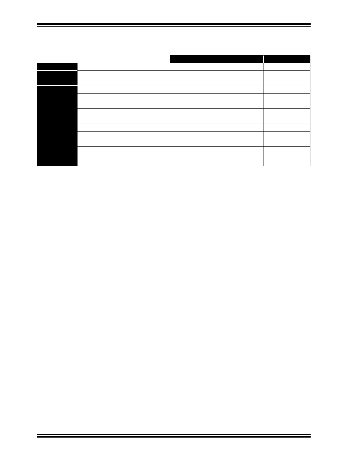
a description of the device pins in Table 3-1.
PIC16CE62X
DS40182D-page 8
1998-2013 Microchip Technology Inc.
FIGURE 3-1:
BLOCK DIAGRAM
EPROM
Program
Memory
13
Data Bus
8
14
Program
Bus
Instruction reg
Program Counter
8 Level Stack
(13-bit)
RAM
File
Registers
Direct Addr
7
RAM Addr
(1)
9
Addr MUX
Indirect
Addr
FSR reg
STATUS reg
MUX
ALU
W reg
Power-up
Timer
Oscillator
Start-up Timer
Power-on
Reset
Watchdog
Timer
Instruction
Decode &
Control
Timing
Generation
OSC1/CLKIN
OSC2/CLKOUT
MCLR/V
PP
V
DD
, V
SS
Voltage
Brown-out
Reset
Note 1:
Higher order bits are from the STATUS register.
Device
Program Memory
Data Memory
(RAM)
EEPROM DATA
MEMORY
PIC16CE623
PIC16CE624
PIC16CE625
512 x 14
1K x 14
2K x 14
96 x 8
96 x 8
128 x 8
128 x 8
128 x 8
128 x 8
8
3
TMR0
I/O Ports
PORTB
Comparator
RA3/AN3
RA2/AN2/V
REF
RA1/AN1
RA0/AN0
Reference
RA4/T0CKI
+
-
+
-
EEPROM
Data
Memory
128 x 8
EEV
DD
EESDA
EEINTF
EESCL
1998-2013 Microchip Technology Inc.
DS40182D-page 9
PIC16CE62X
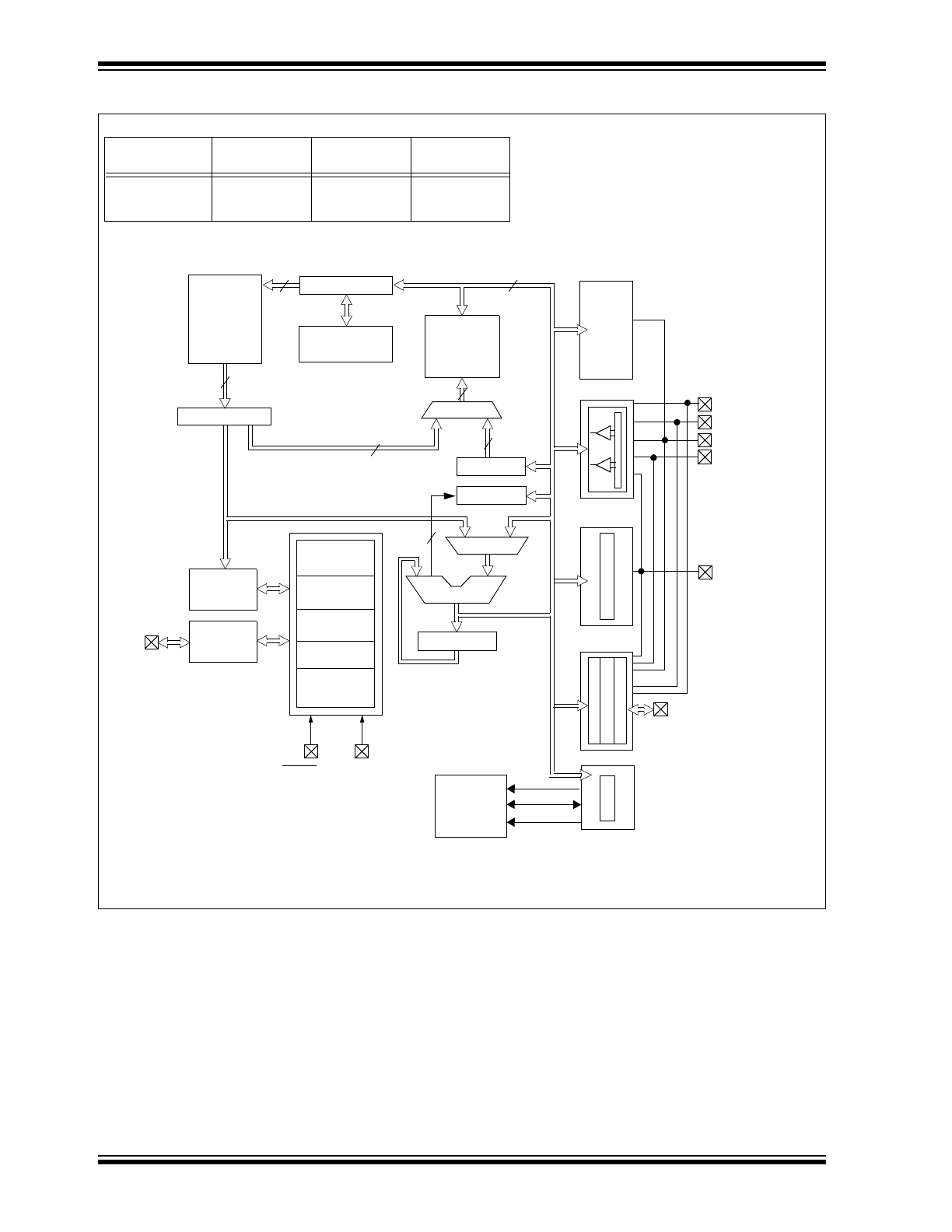
TABLE 3-1:
PIC16CE62X PINOUT DESCRIPTION
Name
DIP/
SOIC
Pin #
SSOP
Pin #
I/O/P
Type
Buffer
Type
Description
OSC1/CLKIN
16
18
I
ST/CMOS Oscillator crystal input/external clock source input.
OSC2/CLKOUT
15
17
O
—
Oscillator crystal output. Connects to crystal or resonator
in crystal oscillator mode. In RC mode, OSC2 pin outputs
CLKOUT which has 1/4 the frequency of OSC1, and
denotes the instruction cycle rate.
MCLR/V
PP
4
4
I/P
ST
Master clear (reset) input/programming voltage input.
This pin is an active low reset to the device.
PORTA is a bi-directional I/O port.
RA0/AN0
17
19
I/O
ST
Analog comparator input
RA1/AN1
18
20
I/O
ST
Analog comparator input
RA2/AN2/V
REF
1
1
I/O
ST
Analog comparator input or V
REF
output
RA3/AN3
2
2
I/O
ST
Analog comparator input /output
RA4/T0CKI
3
3
I/O
ST
Can be selected to be the clock input to the Timer0
timer/counter or a comparator output. Output is open
drain type.
PORTB is a bi-directional I/O port. PORTB can be
software programmed for internal weak pull-up on all
inputs.
RB0/INT
6
7
I/O
TTL/ST
(1)
RB0/INT can also be selected as an external
interrupt pin.
RB1
7
8
I/O
TTL
RB2
8
9
I/O
TTL
RB3
9
10
I/O
TTL
RB4
10
11
I/O
TTL
Interrupt on change pin.
RB5
11
12
I/O
TTL
Interrupt on change pin.
RB6
12
13
I/O
TTL/ST
(2)
Interrupt on change pin. Serial programming clock.
RB7
13
14
I/O
TTL/ST
(2)
Interrupt on change pin. Serial programming data.
V
SS
5
5,6
P
—
Ground reference for logic and I/O pins.
V
DD
14
15,16
P
—
Positive supply for logic and I/O pins.
Legend:
O = output
I/O = input/output
P = power
— = Not used
I = Input
ST = Schmitt Trigger input
TTL = TTL input
Note 1: This buffer is a Schmitt Trigger input when configured as the external interrupt.
Note 2: This buffer is a Schmitt Trigger input when used in serial programming mode.
PIC16CE62X
DS40182D-page 10
1998-2013 Microchip Technology Inc.
3.1
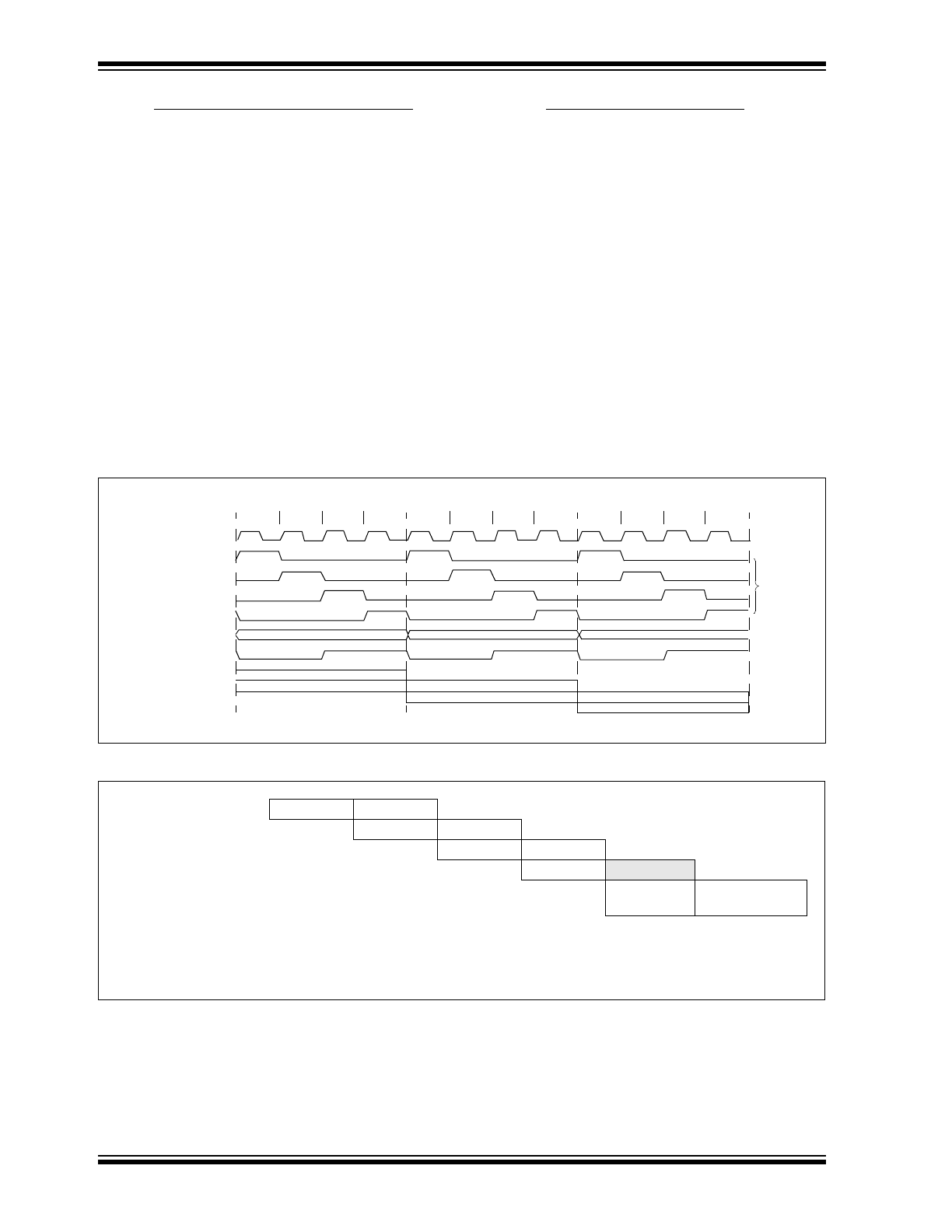
Clocking Scheme/Instruction Cycle
The clock input (OSC1/CLKIN pin) is internally divided
by four to generate four non-overlapping quadrature
clocks namely Q1, Q2, Q3 and Q4. Internally, the
program counter (PC) is incremented every Q1, the
instruction is fetched from the program memory and
latched into the instruction register in Q4. The
instruction is decoded and executed during the
following Q1 through Q4. The clocks and instruction
execution flow is shown in Figure 3-2.
3.2
Instruction Flow/Pipelining
An “Instruction Cycle” consists of four Q cycles (Q1,
Q2, Q3 and Q4). The instruction fetch and execute are
pipelined such that fetch takes one instruction cycle,
while decode and execute takes another instruction
cycle. However, due to the pipelining, each instruction
effectively executes in one cycle. If an instruction
causes the program counter to change (i.e., GOTO) then
two cycles are required to complete the instruction
(Example 3-1).
A fetch cycle begins with the program counter (PC)
incrementing in Q1.
In the execution cycle, the fetched instruction is latched
into the “Instruction Register (IR)” in cycle Q1. This
instruction is then decoded and executed during the
Q2, Q3, and Q4 cycles. Data memory is read during Q2
(operand read) and written during Q4 (destination
write).
FIGURE 3-2:
CLOCK/INSTRUCTION CYCLE
EXAMPLE 3-1:
INSTRUCTION PIPELINE FLOW
Q1
Q2
Q3
Q4
Q1
Q2
Q3
Q4
Q1
Q2
Q3
Q4
OSC1
Q1
Q2
Q3
Q4
PC
OSC2/CLKOUT
(RC mode)
PC
PC+1
PC+2
Fetch INST (PC)
Execute INST (PC-1)
Fetch INST (PC+1)
Execute INST (PC)
Fetch INST (PC+2)
Execute INST (PC+1)
Internal
phase
clock
All instructions are single cycle, except for any program branches. These take two cycles since the fetch instruction is “flushed”
from the pipeline, while the new instruction is being fetched and then executed.
1. MOVLW 55h
Fetch 1
Execute 1
2. MOVWF PORTB
Fetch 2
Execute 2
3. CALL SUB_1
Fetch 3
Execute 3
4. BSF PORTA, BIT3
Fetch 4
Flush
5. Instruction @
address SUB_1
Fetch SUB_1
Execute SUB_1