

NOTE: This is a summary document.
The complete document is available on
the Atmel website at
www.atmel.com.
Features
•
Incorporates the ARM7TDMI
®
ARM
®
Thumb
®
Processor
– High-performance 32-bit RISC Architecture
– High-density 16-bit Instruction Set
– Leader in MIPS/Watt
– EmbeddedICE
™
In-circuit Emulation, Debug Communication Channel Support
•
Internal High-speed Flash
– 512 Kbytes, Organized in Two Contiguous Banks of 1024 Pages of 256 Bytes Dual
Plane (SAM7SE512)
– 256 Kbytes (SAM7SE256) Organized in One Bank of 1024 Pages of 256 Bytes
Single Plane (SAM7SE256)
– 32 Kbytes (SAM7SE32) Organized in One Bank of 256 Pages of 128 Bytes Single
Plane (SAM7SE32)
– Single Cycle Access at Up to 30 MHz in Worst Case Conditions
– Prefetch Buffer Optimizing Thumb Instruction Execution at Maximum Speed
– Page Programming Time: 6 ms, Including Page Auto-erase, Full Erase Time: 15 ms
– 10,000 Erase Cycles, 10-year Data Retention Capability, Sector Lock Capabilities,
Flash Security Bit
– Fast Flash Programming Interface for High Volume Production
•
32 Kbytes (SAM7SE512/256) or 8 Kbytes (SAM7SE32) of Internal
High-speed SRAM, Single-cycle Access at Maximum Speed
•
One External Bus Interface (EBI)
– Supports SDRAM, Static Memory, Glueless Connection to CompactFlash
®
and
ECC-enabled NAND Flash
•
Memory Controller (MC)
– Embedded Flash Controller
– Memory Protection Unit
– Abort Status and Misalignment Detection
•
Reset Controller (RSTC)
– Based on Power-on Reset Cells and Low-power Factory-calibrated Brownout
Detector
– Provides External Reset Signal Shaping and Reset Source Status
•
Clock Generator (CKGR)
– Low-power RC Oscillator, 3 to 20 MHz On-chip Oscillator and One PLL
•
Power Management Controller (PMC)
– Power Optimization Capabilities, Including Slow Clock Mode (Down to 500 Hz) and
Idle Mode
– Three Programmable External Clock Signals
•
Advanced Interrupt Controller (AIC)
– Individually Maskable, Eight-level Priority, Vectored Interrupt Sources
– Two External Interrupt Sources and One Fast Interrupt Source, Spurious Interrupt
Protected
•
Debug Unit (DBGU)
– Two-wire UART and Support for Debug Communication Channel interrupt,
Programmable ICE Access Prevention
– Mode for General Purpose Two-wire UART Serial Communication
•
Periodic Interval Timer (PIT)
– 20-bit Programmable Counter plus 12-bit Interval Counter
•
Windowed Watchdog (WDT)
– 12-bit key-protected Programmable Counter
AT91SAM
ARM-based
Flash MCU
SAM7SE512
SAM7SE256
SAM7SE32
Summary
6222GS–ATARM–6-Sep-11

2
6222GS–ATARM–6-Sep-11
SAM7SE512/256/32 Summary
– Provides Reset or Interrupt Signals to the System
– Counter May Be Stopped While the Processor is in Debug State or in Idle Mode
•
Real-time Timer (RTT)
– 32-bit Free-running Counter with Alarm
– Runs Off the Internal RC Oscillator
•
Three Parallel Input/Output Controllers (PIO)
– Eighty-eight Programmable I/O Lines Multiplexed with up to Two Peripheral I/Os
– Input Change Interrupt Capability on Each I/O Line
– Individually Programmable Open-drain, Pull-up Resistor and Synchronous Output
– Schmitt Trigger on All inputs
•
Eleven Peripheral DMA Controller (PDC) Channels
•
One USB 2.0 Full Speed (12 Mbits per second) Device Port
– On-chip Transceiver, Eight Endpoints, 2688-byte Configurable Integrated FIFOs
•
One Synchronous Serial Controller (SSC)
– Independent Clock and Frame Sync Signals for Each Receiver and Transmitter
– I²S Analog Interface Support, Time Division Multiplex Support
– High-speed Continuous Data Stream Capabilities with 32-bit Data Transfer
•
Two Universal Synchronous/Asynchronous Receiver Transmitters (USART)
– Individual Baud Rate Generator, IrDA
®
Infrared Modulation/Demodulation
– Support for ISO7816 T0/T1 Smart Card, Hardware Handshaking, RS485 Support
– Full Modem Line Support on USART1
•
One Master/Slave Serial Peripheral Interfaces (SPI)
– 8- to 16-bit Programmable Data Length, Four External Peripheral Chip Selects
•
One Three-channel 16-bit Timer/Counter (TC)
– Three External Clock Inputs, Two Multi-purpose I/O Pins per Channel
– Double PWM Generation, Capture/Waveform Mode, Up/Down Capability
•
One Four-channel 16-bit PWM Controller (PWMC)
•
One Two-wire Interface (TWI)
– Master, Multi-Master and Slave Mode Support, All Two-wire Atmel EEPROMs Supported
– General Call Supported in Slave Mode
•
One 8-channel 10-bit Analog-to-Digital Converter, Four Channels Multiplexed with Digital I/Os
•
SAM-BA
®
– Default Boot program
– Interface with SAM-BA Graphic User Interface
•
IEEE
®
1149.1 JTAG Boundary Scan on All Digital Pins
•
Four High-current Drive I/O lines, Up to 16 mA Each
•
Power Supplies
– Embedded 1.8V Regulator, Drawing up to 100 mA for the Core and External Components
– 1.8V or 3,3V VDDIO I/O Lines Power Supply, Independent 3.3V VDDFLASH Flash Power Supply
– 1.8V VDDCORE Core Power Supply with Brownout Detector
•
Fully Static Operation:
– Up to 55 MHz at 1.8V and 85
° C Worst Case Conditions
– Up to 48 MHz at 1.65V and 85
° C Worst Case Conditions
•
Available in a 128-lead LQFP Green Package, or a 144-ball LFBGA RoHS-compliant Package
3
6222GS–ATARM–6-Sep-11
SAM7SE512/256/32 Summary
1.
Description
Atmel's SAM7SE Series is a member of its Smart ARM Microcontroller family based on the 32-
bit ARM7
™
RISC processor and high-speed Flash memory.
• SAM7SE512 features a 512-Kbyte high-speed Flash and a 32 Kbyte SRAM.
• SAM7SE256 features a 256-Kbyte high-speed Flash and a 32 Kbyte SRAM.
• SAM7SE32 features a 32-Kbyte high-speed Flash and an 8 Kbyte SRAM.
It also embeds a large set of peripherals, including a USB 2.0 device, an External Bus Interface
(EBI), and a complete set of system functions minimizing the number of external components.
The EBI incorporates controllers for synchronous DRAM (SDRAM) and Static memories and
features specific circuitry facilitating the interface for NAND Flash, SmartMedia and
CompactFlash.
The device is an ideal migration path for 8/16-bit microcontroller users looking for additional per-
formance, extended memory and higher levels of system integration.
The embedded Flash memory can be programmed in-system via the JTAG-ICE interface or via
a parallel interface on a production programmer prior to mounting. Built-in lock bits and a secu-
rity bit protect the firmware from accidental overwrite and preserve its confidentiality.
The SAM7SE Series system controller includes a reset controller capable of managing the
power-on sequence of the microcontroller and the complete system. Correct device operation
can be monitored by a built-in brownout detector and a watchdog running off an integrated RC
oscillator.
By combining the ARM7TDMI processor with on-chip Flash and SRAM, and a wide range of
peripheral functions, including USART, SPI, External Bus Interface, Timer Counter, RTT and
Analog-to-Digital Converters on a monolithic chip, the SAM7SE512/256/32 is a powerful device
that provides a flexible, cost-effective solution to many embedded control applications.
1.1
Configuration Summary of the SAM7SE512, SAM7SE256 and SAM7SE32
The SAM7SE512, SAM7SE256 and SAM7SE32 differ in memory sizes and organization.
Table
1-1
below summarizes the configurations for the three devices.
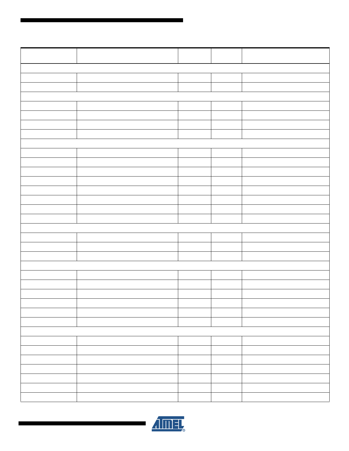
Table 1-1.
Configuration Summary
Device
Flash Size
Flash Organization
RAM Size
SAM7SE512
512K bytes
dual plane
32K bytes
SAM7SE256
256K bytes
single plane
32K bytes
SAM7SE32
32K bytes
single plane
8K bytes
4
6222GS–ATARM–6-Sep-11
SAM7SE512/256/32 Summary
2.
Block Diagram
Figure 2-1.
SAM7SE512/256/32 Block Diagram Signal Description
Reset
Controller
PMC
APB
ICE
JTAG
SCAN
ARM7TDMI
Processor
System Controller
AIC
DBGU
PDC
PDC
PLL
OSC
RCOSC
BOD
POR
PIO
PIT
WDT
RTT
PIOA
PIOB
PIOC
PIO
PIO
PIO
USART0
USART1
SPI
Timer Counter
PDC
PDC
PDC
PDC
PDC
PDC
PDC
PDC
TC0
TC1
TC2
ADC
ADVREF
TWI
SSC
PWMC
USB Device
FIFO
Static Memory
Controller
ECC
Controller
SDRAM
Controller
EBI
CompactFlash
NAND Flash
SRAM
32 Kbytes (SE512/256)
or
8 Kbytes (SE32)
Flash
512 Kbytes (SE512)
256 Kbytes (SE256)
32 Kbytes (SE32)
1.8V
Voltage
Regulator
Memory Controller
Embedded
Flash
Controller
Address
Decoder
Abort
Status
Misalignment
Detection
Memory Protection
Unit
Peripheral DMA
Controller
11 Channels
Peripheral Bridge
Fast Flash
Programming
Interface
SAM-BA
Tr
anscie
ve
r
PDC
ROM
NPCS0
NPCS1
NPCS2
NPCS3
MISO
MOSI
SPCK
TIOA0
TIOB0
TIOA1
TIOB1
TIOA2
TIOB2
ADTRG
AD0
AD1
AD2
AD3
AD4
AD5
AD6
AD7
TCLK0
TCLK1
TCLK2
RXD0
TXD0
SCK0
RTS0
CTS0
RXD1
TXD1
SCK1
RTS1
CTS1
DCD1
DSR1
DTR1
RI1
NRST
VDDCORE
VDDCORE
VDDFLASH
XIN
XOUT
PLLRC
PCK0-PCK2
DRXD
DTXD
IRQ0-IRQ1
FIQ
TST
TDI
TDO
TMS
TCK
JTAGSEL
VDDIN
GND
VDDOUT
VDDCORE
VDDIO
VDDFLASH
ERASE
PGMRDY
PGMNVALID
PGMNOE
PGMCK
PGMM0-PGMM3
PGMD0-PGMD15
PGMNCMD
PGMEN0-PGMEN1
D[31:0]
A0/NBS0
A1/NBS2
A[15:2], A[20:18]
A21/NANDALE
A22/REG/NANDCLE
A16/BA0
A17/BA1
NCS0
NCS1/SDCS
NCS2/CFCS1
NCS3/NANDCS
NRD/CFOE
NWR0/NWE/CFWE
NWR1/NBS1/CFIOR
NBS3/CFIOW
SDCKE
RAS
CAS
SDWE
SDA10
CFRNW
NCS4/CFCS0
NCS5/CFCE1
NCS6/CFCE2
NCS7
NANDOE
NANDWE
NWAIT
SDCK
DDM
DDP
PWM0
PWM1
PWM2
PWM3
TF
TK
TD
RD
RK
RF
TWD
TWCK
5
6222GS–ATARM–6-Sep-11
SAM7SE512/256/32 Summary
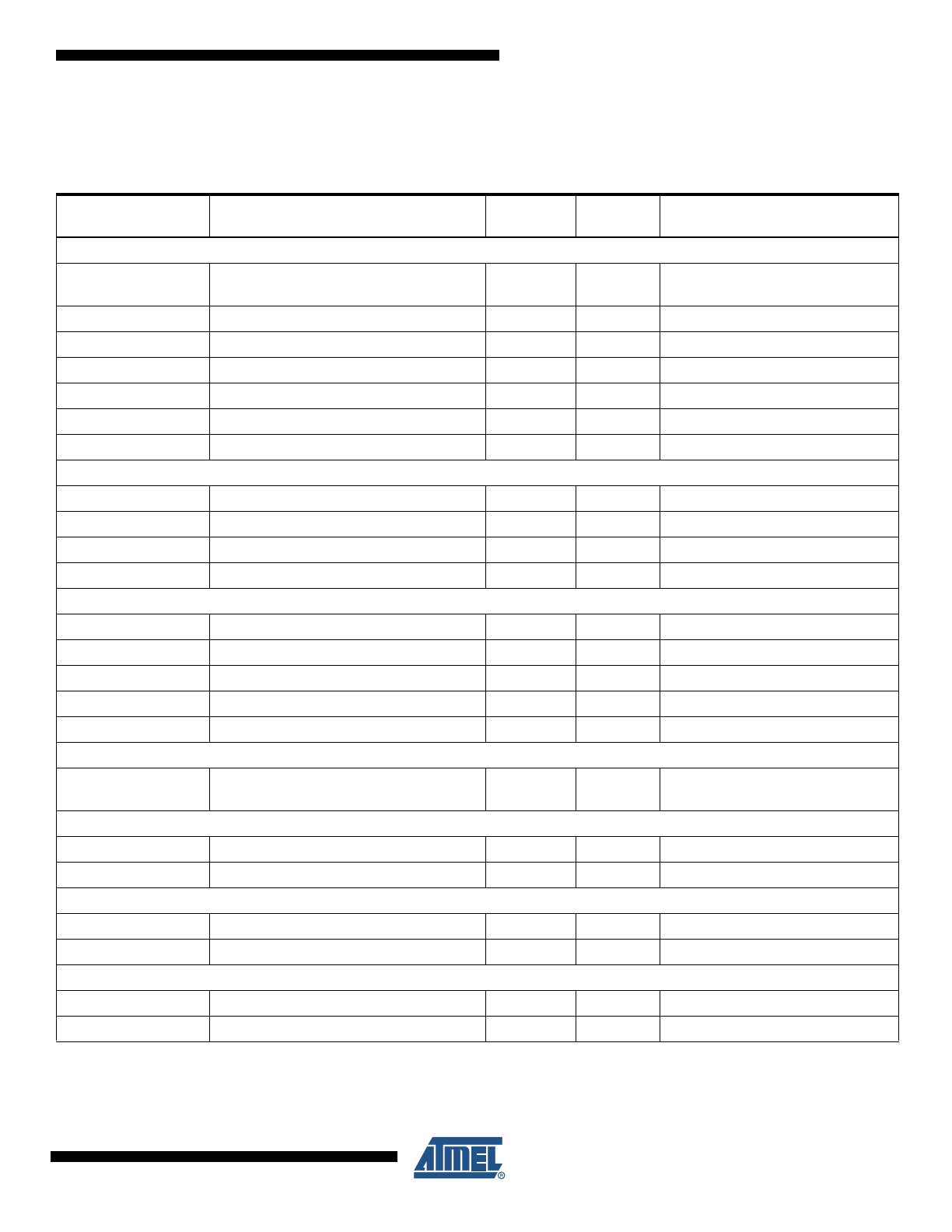
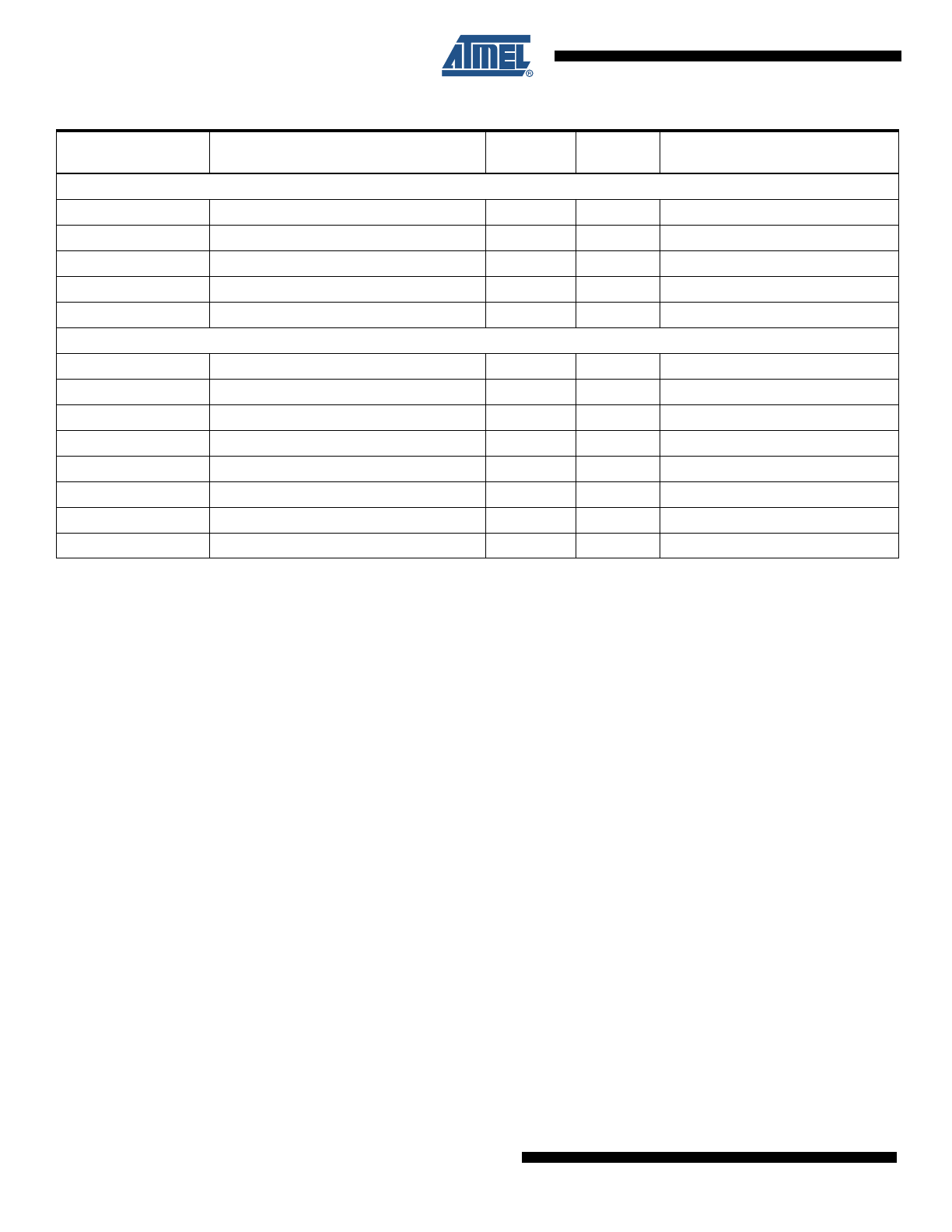
3.
Signal Description
Table 3-1.
Signal Description List
Signal Name
Function
Type
Active
Level
Comments
Power
VDDIN
Voltage Regulator and ADC Power
Supply Input
Power
3V to 3.6V
VDDOUT
Voltage Regulator Output
Power
1.85V
VDDFLASH
Flash and USB Power Supply
Power
3V to 3.6V
VDDIO
I/O Lines Power Supply
Power
3V to 3.6V or 1.65V to 1.95V
VDDCORE
Core Power Supply
Power
1.65V to 1.95V
VDDPLL
PLL
Power
1.65V to 1.95V
GND
Ground
Ground
Clocks, Oscillators and PLLs
XIN
Main Oscillator Input
Input
XOUT
Main Oscillator Output
Output
PLLRC
PLL Filter
Input
PCK0 - PCK2
Programmable Clock Output
Output
ICE and JTAG
TCK
Test Clock
Input
No pull-up resistor
TDI
Test Data In
Input
No pull-up resistor
TDO
Test Data Out
Output
TMS
Test Mode Select
Input
No pull-up resistor.
JTAGSEL
JTAG Selection
Input
Pull-down resistor
(1)
Flash Memory
ERASE
Flash and NVM Configuration Bits Erase
Command
Input
High
Pull-down resistor
(1)
Reset/Test
NRST
Microcontroller Reset
I/O
Low
Open drain with pull-up resistor
(1)
TST
Test Mode Select
Input
High
Pull-down resistor
(1)
Debug Unit
DRXD
Debug Receive Data
Input
DTXD
Debug Transmit Data
Output
AIC
IRQ0 - IRQ1
External Interrupt Inputs
Input
FIQ
Fast Interrupt Input
Input
6
6222GS–ATARM–6-Sep-11
SAM7SE512/256/32 Summary
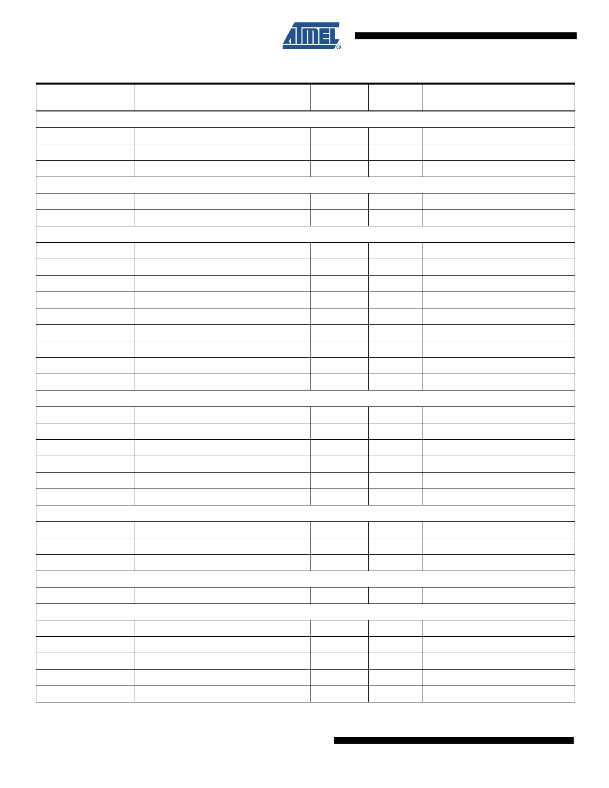
PIO
PA0 - PA31
Parallel IO Controller A
I/O
Pulled-up input at reset
PB0 - PB31
Parallel IO Controller B
I/O
Pulled-up input at reset
PC0 - PC23
Parallel IO Controller C
I/O
Pulled-up input at reset
USB Device Port
DDM
USB Device Port Data -
Analog
DDP
USB Device Port Data +
Analog
USART
SCK0 - SCK1
Serial Clock
I/O
TXD0 - TXD1
Transmit Data
I/O
RXD0 - RXD1
Receive Data
Input
RTS0 - RTS1
Request To Send
Output
CTS0 - CTS1
Clear To Send
Input
DCD1
Data Carrier Detect
Input
DTR1
Data Terminal Ready
Output
DSR1
Data Set Ready
Input
RI1
Ring Indicator
Input
Synchronous Serial Controller
TD
Transmit Data
Output
RD
Receive Data
Input
TK
Transmit Clock
I/O
RK
Receive Clock
I/O
TF
Transmit Frame Sync
I/O
RF
Receive Frame Sync
I/O
Timer/Counter
TCLK0 - TCLK2
External Clock Inputs
Input
TIOA0 - TIOA2
Timer Counter I/O Line A
I/O
TIOB0 - TIOB2
Timer Counter I/O Line B
I/O
PWM Controller
PWM0 - PWM3
PWM Channels
Output
Serial Peripheral Interface
MISO
Master In Slave Out
I/O
MOSI
Master Out Slave In
I/O
SPCK
SPI Serial Clock
I/O
NPCS0
SPI Peripheral Chip Select 0
I/O
Low
NPCS1-NPCS3
SPI Peripheral Chip Select 1 to 3
Output
Low
Table 3-1.
Signal Description List (Continued)
Signal Name
Function
Type
Active
Level
Comments
7
6222GS–ATARM–6-Sep-11
SAM7SE512/256/32 Summary
Two-Wire Interface
TWD
Two-wire Serial Data
I/O
TWCK
Two-wire Serial Clock
I/O
Analog-to-Digital Converter
AD0-AD3
Analog Inputs
Analog
Digital pulled-up inputs at reset
AD4-AD7
Analog Inputs
Analog
Analog Inputs
ADTRG
ADC Trigger
Input
ADVREF
ADC Reference
Analog
Fast Flash Programming Interface
PGMEN0-PGMEN2
Programming Enabling
Input
PGMM0-PGMM3
Programming Mode
Input
PGMD0-PGMD15
Programming Data
I/O
PGMRDY
Programming Ready
Output
High
PGMNVALID
Data Direction
Output
Low
PGMNOE
Programming Read
Input
Low
PGMCK
Programming Clock
Input
PGMNCMD
Programming Command
Input
Low
External Bus Interface
D[31:0]
Data Bus
I/O
A[22:0]
Address Bus
Output
NWAIT
External Wait Signal
Input
Low
Static Memory Controller
NCS[7:0]
Chip Select Lines
Output
Low
NWR[1:0]
Write Signals
Output
Low
NRD
Read Signal
Output
Low
NWE
Write Enable
Output
Low
NUB
NUB: Upper Byte Select
Output
Low
NLB
NLB: Lower Byte Select
Output
Low
EBI for CompactFlash Support
CFCE[2:1]
CompactFlash Chip Enable
Output
Low
CFOE
CompactFlash Output Enable
Output
Low
CFWE
CompactFlash Write Enable
Output
Low
CFIOR
CompactFlash I/O Read Signal
Output
Low
CFIOW
CompactFlash I/O Write Signal
Output
Low
CFRNW
CompactFlash Read Not Write Signal
Output
CFCS[1:0]
CompactFlash Chip Select Lines
Output
Low
Table 3-1.
Signal Description List (Continued)
Signal Name
Function
Type
Active
Level
Comments
8
6222GS–ATARM–6-Sep-11
SAM7SE512/256/32 Summary
Note:
1. Refer to
Section 6. “/O Lines Considerations” on page 15
.
EBI for NAND Flash Support
NANDCS
NAND Flash Chip Select Line
Output
Low
NANDOE
NAND Flash Output Enable
Output
Low
NANDWE
NAND Flash Write Enable
Output
Low
NANDCLE
NAND Flash Command Line Enable
Output
Low
NANDALE
NAND Flash Address Line Enable
Output
Low
SDRAM Controller
SDCK
SDRAM Clock
Output
Tied low after reset
SDCKE
SDRAM Clock Enable
Output
High
SDCS
SDRAM Controller Chip Select Line
Output
Low
BA[1:0]
Bank Select
Output
SDWE
SDRAM Write Enable
Output
Low
RAS - CAS
Row and Column Signal
Output
Low
NBS[3:0]
Byte Mask Signals
Output
Low
SDA10
SDRAM Address 10 Line
Output
Table 3-1.
Signal Description List (Continued)
Signal Name
Function
Type
Active
Level
Comments
9
6222GS–ATARM–6-Sep-11
SAM7SE512/256/32 Summary
4.
Package
The SAM7SE512/256/32 is available in:
• 20 x 14 mm 128-lead LQFP package with a 0.5 mm lead pitch.
• 10x 10 x 1.4 mm 144-ball LFBGA package with a 0.8 mm lead pitch
4.1
128-lead LQFP Package Outline
Figure 4-1
shows the orientation of the 128-lead LQFP package and a detailed mechanical
description is given in the Mechanical Characteristics section of the full datasheet.
Figure 4-1.
128-lead LQFP Package Outline (Top View)
65
103
102
64
39
38
1
128
10
6222GS–ATARM–6-Sep-11
SAM7SE512/256/32 Summary
4.2
128-lead LQFP Pinout
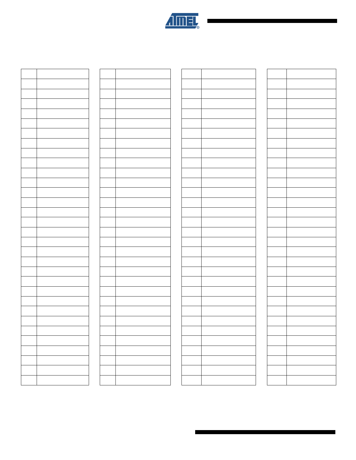
Table 4-1.
Pinout in 128-lead LQFP Package
1
ADVREF
33
PB31
65
TDI
97
SDCK
2
GND
34
PB30
66
TDO
98
PC8
3
AD7
35
PB29
67
PB2
99
PC7
4
AD6
36
PB28
68
PB1
100
PC6
5
AD5
37
PB27
69
PB0
101
PC5
6
AD4
38
PB26
70
GND
102
PC4
7
VDDOUT
39
PB25
71
VDDIO
103
PC3
8
VDDIN
40
PB24
72
VDDCORE
104
PC2
9
PA20/PGMD8/AD3
41
PB23
73
NRST
105
PC1
10
PA19/PGMD7/AD2
42
PB22
74
TST
106
PC0
11
PA18/PGMD6/AD1
43
PB21
75
ERASE
107
PA31
12
PA17/PGMD5/AD0
44
PB20
76
TCK
108
PA30
13
PA16/PGMD4
45
GND
77
TMS
109
PA29
14
PA15/PGMD3
46
VDDIO
78
JTAGSEL
110
PA28
15
PA14/PGMD2
47
VDDCORE
79
PC23
111
PA27/PGMD15
16
PA13/PGMD1
48
PB19
80
PC22
112
PA26/PGMD14
17
PA12/PGMD0
49
PB18
81
PC21
113
PA25/PGMD13
18
PA11/PGMM3
50
PB17
82
PC20
114
PA24/PGMD12
19
PA10/PGMM2
51
PB16
83
PC19
115
PA23/PGMD11
20
PA9/PGMM1
52
PB15
84
PC18
116
PA22/PGMD10
21
VDDIO
53
PB14
85
PC17
117
PA21/PGMD9
22
GND
54
PB13
86
PC16
118
VDDCORE
23
VDDCORE
55
PB12
87
PC15
119
GND
24
PA8/PGMM0
56
PB11
88
PC14
120
VDDIO
25
PA7/PGMNVALID
57
PB10
89
PC13
121
DM
26
PA6/PGMNOE
58
PB9
90
PC12
122
DP
27
PA5/PGMRDY
59
PB8
91
PC11
123
VDDFLASH
28
PA4/PGMNCMD
60
PB7
92
PC10
124
GND
29
PA3
61
PB6
93
PC9
125
XIN/PGMCK
30
PA2/PGMEN2
62
PB5
94
GND
126
XOUT
31
PA1/PGMEN1
63
PB4
95
VDDIO
127
PLLRC
32
PA0/PGMEN0
64
PB3
96
VDDCORE
128
VDDPLL