
2017 Microchip Technology Inc.
DS20005531B-page 1
MIC4609
Features
• Gate Drive Supply Voltage up to 20V
• Overcurrent Protection with Programmable
Restart Delay
• 1A Gate Drivers
• Dual (HI/LI) Inputs per Phase
• Fault Signal Asserts on Overcurrent and V
DD
UVLO
• TTL Input Thresholds
• 300 ns Typical Input Filtering Time
• Shoot-Through Protection
• Low Power Consumption
• Supply Undervoltage Protection
• –40°C to +125°C Junction Temperature Range
Typical Applications
• 3-Phase Motor Drive
• Field-Oriented Control (FOC)
• White Goods Appliances
• Brushless DC Fans
General Description
The MIC4609 is a 600V 3-phase MOSFET/IGBT driver.
The MIC4609 features a 300 ns typical input filtering
time to prevent unwanted pulses and a 550 ns of
propagation delay. The MIC4609 has TTL input
thresholds.
The robust operation of the MIC4609 ensures that the
outputs are not affected by supply glitches, High Side
(HS) ringing below ground, or HS slewing with
high-speed voltage transitions. Undervoltage
protection is provided on both the low-side and
high-side drivers.
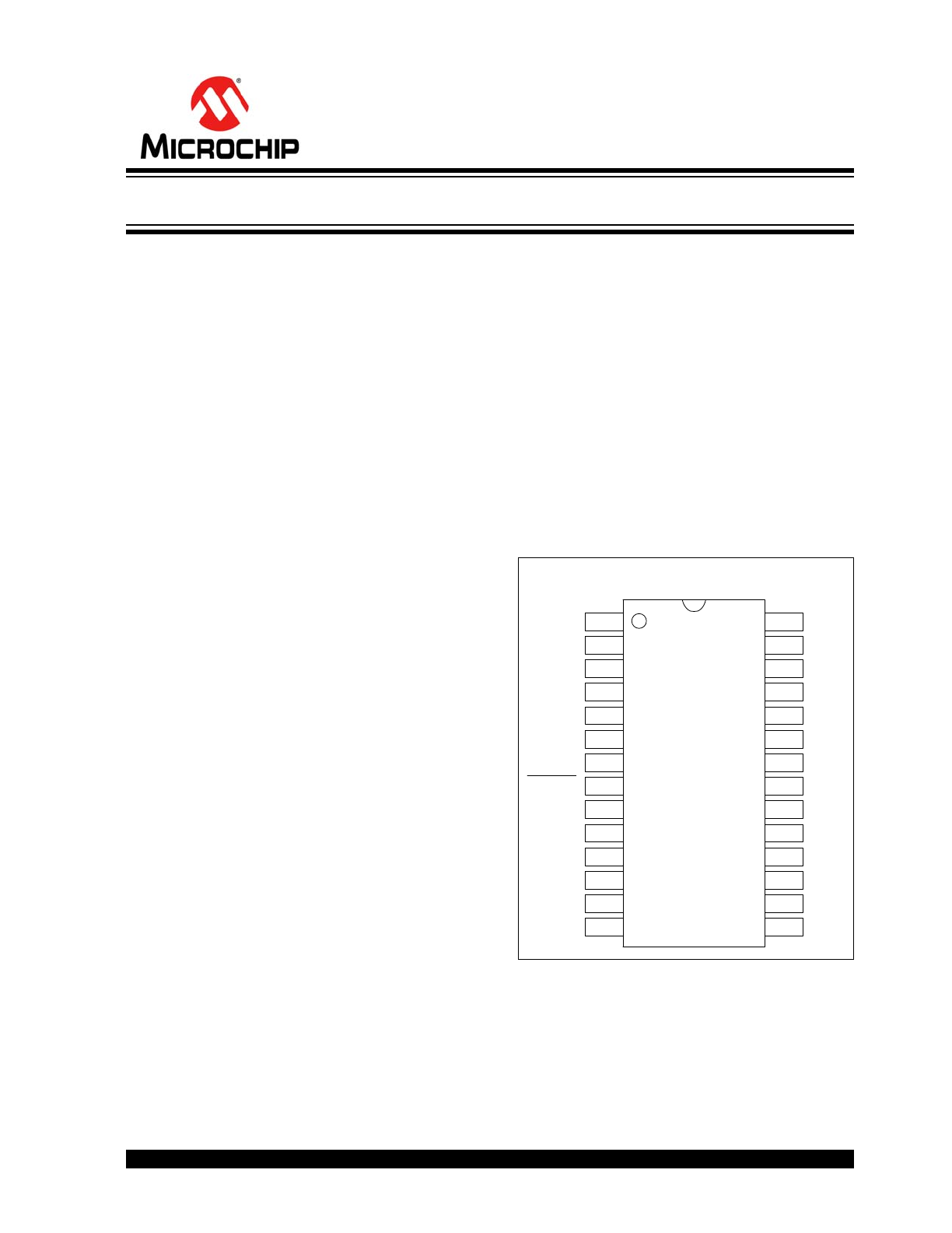
The MIC4609 is available in a 28-pin wide SOIC
package. The MIC4609 has an operating junction
temperature range of –40°C to +125°C.
Package Type
MIC4609
28-Pin SOICW
V
DD
AHI
ALI
BHI
BLI
CHI
FAULT
CLI
EN
ISNS
COM
RCIN
V
SS
CLO
AHB
AHO
BHB
AHS
BHO
NC
NC
BHS
CHO
CHB
ALO
CHS
15
NC
BLO
16
17
18
19
20
21
22
23
24
25
26
27
28
14
13
12
11
10
9
8
7
6
5
4
3
2
1
600V 3-Phase MOSFET/IGBT Driver
MIC4609
DS20005531B-page 2
2017 Microchip Technology Inc.
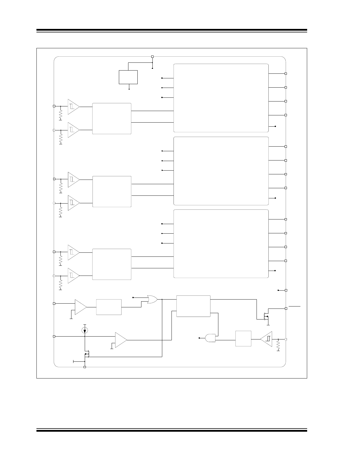
Functional Block Diagram MIC4609 – Top Level Circuit
UVLO
Phase A Drive Circuit
AHB
AHS
AHO
ALO
COM
COM
COM
V
DD
UVLO
V
DD
EN
AHI
ALI
AHI
ALI
Input Filter &
Anti-Shoot-Through
V
DD
UVLO
Phase B Drive Circuit
BHB
BHS
BHO
BLO
UVLO
V
DD
EN
BHI
BLI
Input Filter &
Anti-Shoot-Through
Phase C Drive Circuit
CHB
CHS
CHO
CLO
UVLO
V
DD
EN
CHI
CLI
Input Filter &
Anti-Shoot-Through
COM
COM
ISNS
V
ISNS
Input
Blanking
RCIN
V
SS
I
RCIN
V
RCIN+
+
-
+
-
UVLO
FAULT
EN
V
SS
Input
Filter
EN
Latch
S
R
Q
_
Q
V
SS
V
SS
V
SS
V
SS
V
SS
V
SS
V
SS
V
SS
CHI
CLI
BHI
BLI
2017 Microchip Technology Inc.
DS20005531B-page 3
MIC4609
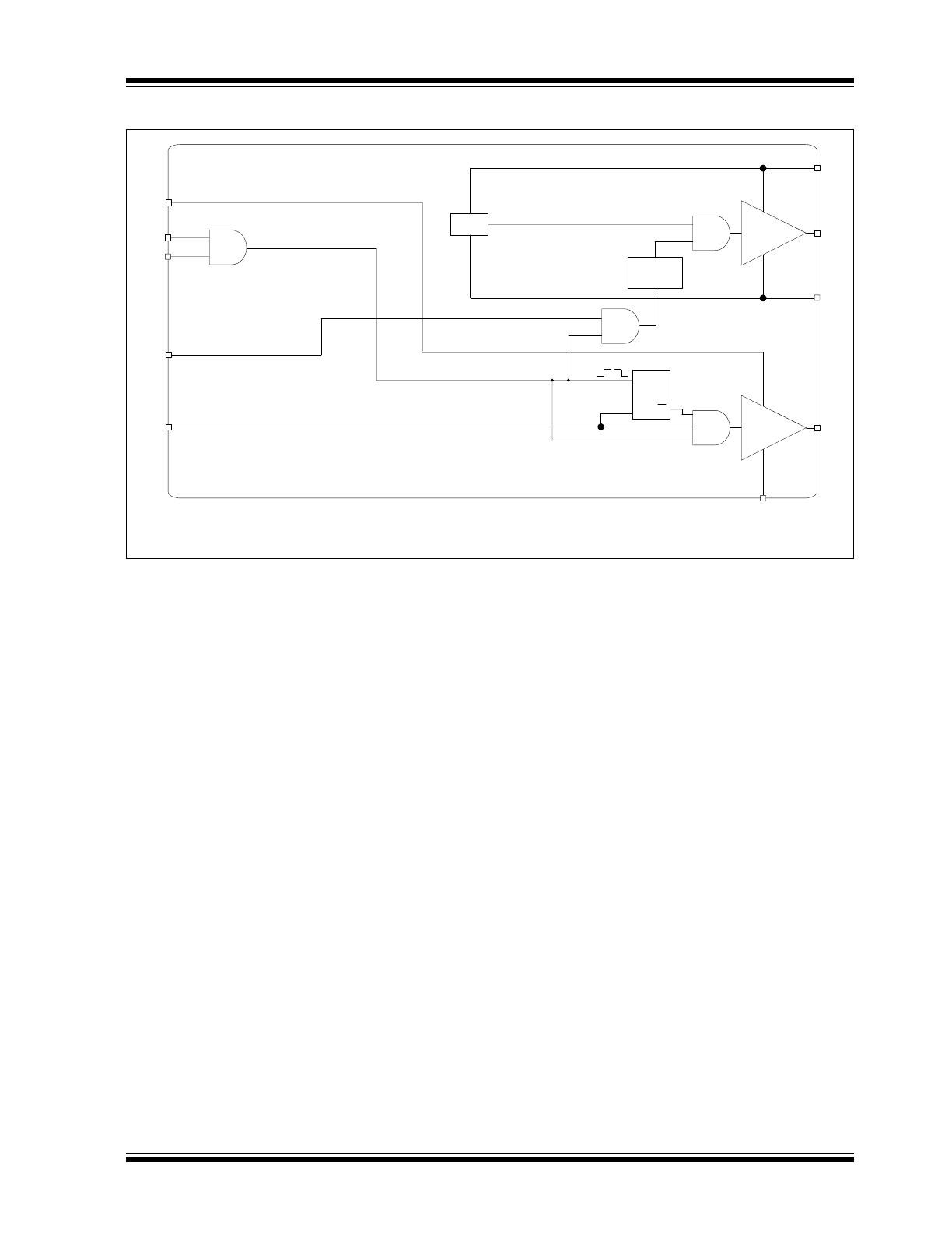
Functional Block Diagram MIC4609 – Phase x Drive Circuit
Note:
The x in the suffix of a pin name designates any of the three phases, e.g., xHS refers to either AHS,
BHS or CHS.
xHB
xHS
xHO
xLO
xHI
xLI
COM
DRIVER
DRIVER
UVLO
LEVEL
SHIFT
V
DD
UVLO
EN
R
Q
S
Q
MIC4609
DS200055
31B-page 4
2017 Microchip T
echnolo
gy Inc.
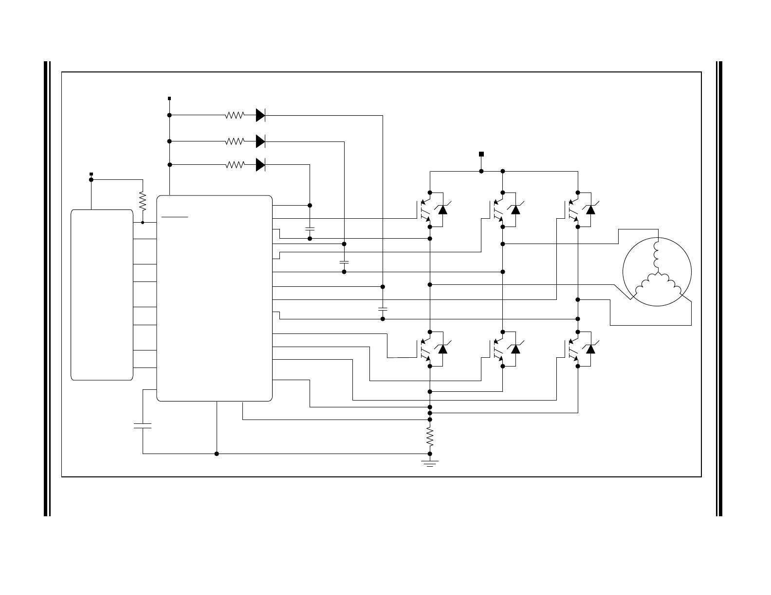
Typical Application Circuit MIC4609 – 300V, 3-Phase Motor Driver
V
DD
BHB
BHO
BHS
BLO
VSS
ALI
AHI
Controller
EN
CHB
CHO
CHS
CLO
BLI
BHI
300V
SUPPLY
AHB
AHO
AHS
ALO
CLI
CHI
FAULT
MIC4609
C1
CDLY
C3
D2
R2
D1
R1
D3
R3
Q1
Q2
Q3
Q4
Q5
Q6
RS
COM
ISNS
RCIN
V
CC
V
DD
C2

2017 Microchip Technology Inc.
DS20005531B-page 5
MIC4609
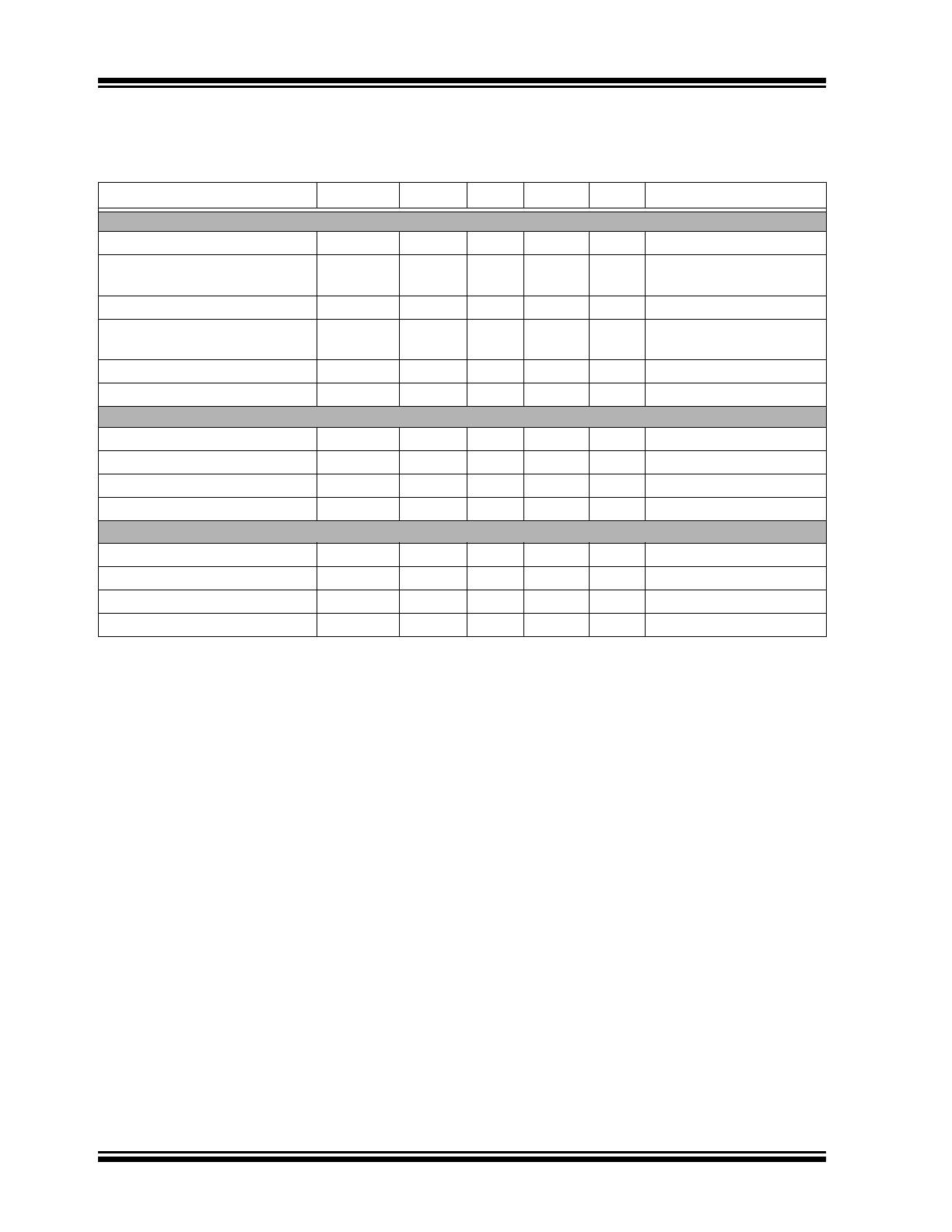
1.0
ELECTRICAL CHARACTERISTICS
Absolute Maximum Ratings †
Supply Voltage (V
DD
, V
xHB
– V
xHS
) ........................................................................................................... –0.3V to +25V
Input Voltages (V
xLI
, V
xHI
, V
EN
).................................................................................................................... –0.3V to V
DD
Voltage on LO (V
xLO
) ................................................................................................................................... –0.3V to V
DD
Voltage on HO (V
xHO
) .......................................................................................................................... V
HS
– 0.3V to V
HB
Voltage on HS ............................................................................................................................................. –5V to +630V
Voltage on HB .........................................................................................................................................................+655V
ESD Rating (HBM)..................................................................................................................................................... 2 kV
ESD Rating (CDM).................................................................................................................................................. 1.5 kV
Operating Ratings ‡
Supply Voltage (V
DD
) .................................................................................................................................. +10V to +20V
Voltage on xHS (continuous) ...................................................................................................................... –1V to +600V
Voltage on xHS (repetitive transient)........................................................................................................... –5V to +600V
HS Slew Rate........................................................................................................................................................ 50 V/ns
Voltage on xHB .......................................................................................................................V
xHS
+ 10V to V
xHS
+ 20V
and/or........................................................................................................................... V
DD
– 1V to V
DD
+ 600V
† Notice:
Stresses above those listed under “Maximum Ratings” may cause permanent damage to the device. This is
a stress rating only and functional operation of the device at those or any other conditions above those indicated in the
operational listings of this specification is not implied. Exposure to maximum rating conditions for extended periods may
affect device reliability.
‡ Notice:
The device is not guaranteed to function outside its operating rating.
MIC4609
DS20005531B-page 6
2017 Microchip Technology Inc.
AC/DC ELECTRICAL CHARACTERISTICS (
Note 1
,
2
)
Electrical Specifications:
Unless otherwise indicated, V
DD
= V
xHB
= 20V, V
EN
= 5V, V
SS
= V
xHS
= 0V; No load on
xLO or xHO, T
A
= +25°C. Bold values indicate –40°C
T
J
+125°C.
Parameter
Symbol
Min.
Typ.
Max.
Units
Conditions
Supply Current
V
DD
Quiescent Current
I
DD
—
150
250
µA
xLI = xHI = 0V
V
DD
Shutdown Current
I
DDSH
—
0.1
10
µA
EN = 0V with HS = floating
or ground
V
DD
Operating Current
I
DDO
—
240
350
µA
f = 20 kHz
Total xHB Quiescent Current
I
xHB
—
81
180
µA
xLI = xHI = 0V or
xLI = 0V and xHI = 5V
Total xHB Operating Current
I
xHBO
—
600
1500
µA
f = 20 kHz
High-Side Leakage Current
I
LxHB
—
1
10
µA
V
xHB
= V
xHS
= 600V
Input (TTL: xLI, xHI, EN)
Low-Level Input Voltage
V
IL
—
—
0.8
V
High-Level Input Voltage
V
IH
2.2
—
—
V
Input Voltage Hysteresis
V
HYS
—
0.2
—
V
Input Pull-Down Resistance
R
I
100
370
500
k
For xLI and xHI only (
Note 3
)
Undervoltage Protection
V
DD
Falling Threshold
V
DDR
7
8
9
V
—
V
DD
Threshold Hysteresis
V
DDH
—
0.5
—
V
—
xHB Falling Threshold
V
xHBR
7
8
9
V
—
xHB Threshold Hysteresis
V
xHBH
—
0.5
—
V
—
Note 1:
Specification for packaged product only.
2:
The x in the suffix of a pin name designates any of the three phases, e.g., xHS refers to either AHS, BHS
or CHS.
3:
Enable resistance is typical only and is not production tested.
2017 Microchip Technology Inc.
DS20005531B-page 7
MIC4609
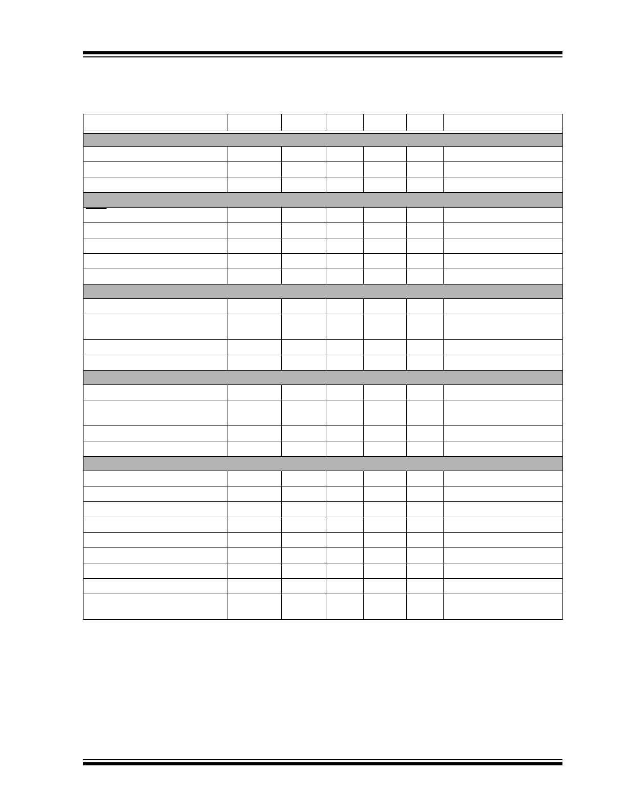
Overcurrent Protection
Rising Overcurrent Threshold
V
ISNS+
420
520
650
mV
—
ISNS Pin Blanking Time
t
ISNS_BLK
270
370
470
ns
—
ISNS-to-Gate Propagation Delay
t
ISNS_PROP
400
650
900
ns
—
Fault Circuit
Fault Pin Output Low Voltage
V
OLF
—
—
0.8
V
V
ISNS
= 1V, I
FAULT
= 1 mA
Rising VCIN Pin Threshold
V
RCIN+
—
5
—
V
—
VCIN Hysteresis
V
RCIN_HYS
—
0.6
—
V
—
RCIN Pin Current Source
I
RCIN
3
5
7
µA
V
RCIN
= 0V
Fault Clear Time
t
FCL
0.5
1
2
ms
C
RCIN
= 1nF
LO Gate Driver
Low-Level Output Voltage
V
xOLL
—
0.5
0.9
V
I
xLO
= 50 mA
High-Level Output Voltage
V
xOHL
—
0.6
0.9
V
I
xLO
= -50 mA
V
xOHL
= V
DD
– V
xLO
Peak Sink Current
I
xOHL
—
1
—
A
V
xLO
= 0V
Peak Source Current
I
xOLL
—
1
—
A
V
xLO
= 20V
HO Gate Driver
Low-Level Output Voltage
V
xOLH
—
0.5
0.9
V
I
xHO
= 50 mA
High-Level Output Voltage
V
xOHH
—
0.6
0.9
V
I
xHO
= –50 mA
V
xOHH
= V
xHB
– V
xHO
Peak Sink Current
I
xOHH
—
1
—
A
V
xHO
= 0V
Peak Source Current
I
xOLH
—
1
—
A
V
xHO
= 20V
Switching Specifications
Turn-On Propagation Delay
t
ON
300
600
700
ns
C
L
= 1 nF
Turn-Off Propagation Delay
t
OFF
300
550
700
ns
C
L
= 1 nF
Turn-On Rise Time
t
R
—
20
60
ns
C
L
= 1 nF
Turn-Off Fall Time
t
F
—
20
60
ns
C
L
= 1 nF
Input Filtering Time
t
FLTR
200
300
480
ns
xLI, xHI, EN
Dead Time
t
D
200
300
450
ns
C
L
= 1 nF
Delay Matching
t
DLYM
—
50
—
ns
C
L
= 1 nF
EN-to-Gate Shutdown Delay
t
EN_OFF
450
650
750
ns
C
L
= 1 nF
Output Pulse Width Matching
t
PWN
—
50
—
ns
t
PW
> 1 µs
C
L
= 1 nF
AC/DC ELECTRICAL CHARACTERISTICS (CONTINUED) (
Note 1
,
2
)
Electrical Specifications:
Unless otherwise indicated, V
DD
= V
xHB
= 20V, V
EN
= 5V, V
SS
= V
xHS
= 0V; No load on
xLO or xHO, T
A
= +25°C. Bold values indicate –40°C
T
J
+125°C.
Parameter
Symbol
Min.
Typ.
Max.
Units
Conditions
Note 1:
Specification for packaged product only.
2:
The x in the suffix of a pin name designates any of the three phases, e.g., xHS refers to either AHS, BHS
or CHS.
3:
Enable resistance is typical only and is not production tested.
MIC4609
DS20005531B-page 8
2017 Microchip Technology Inc.
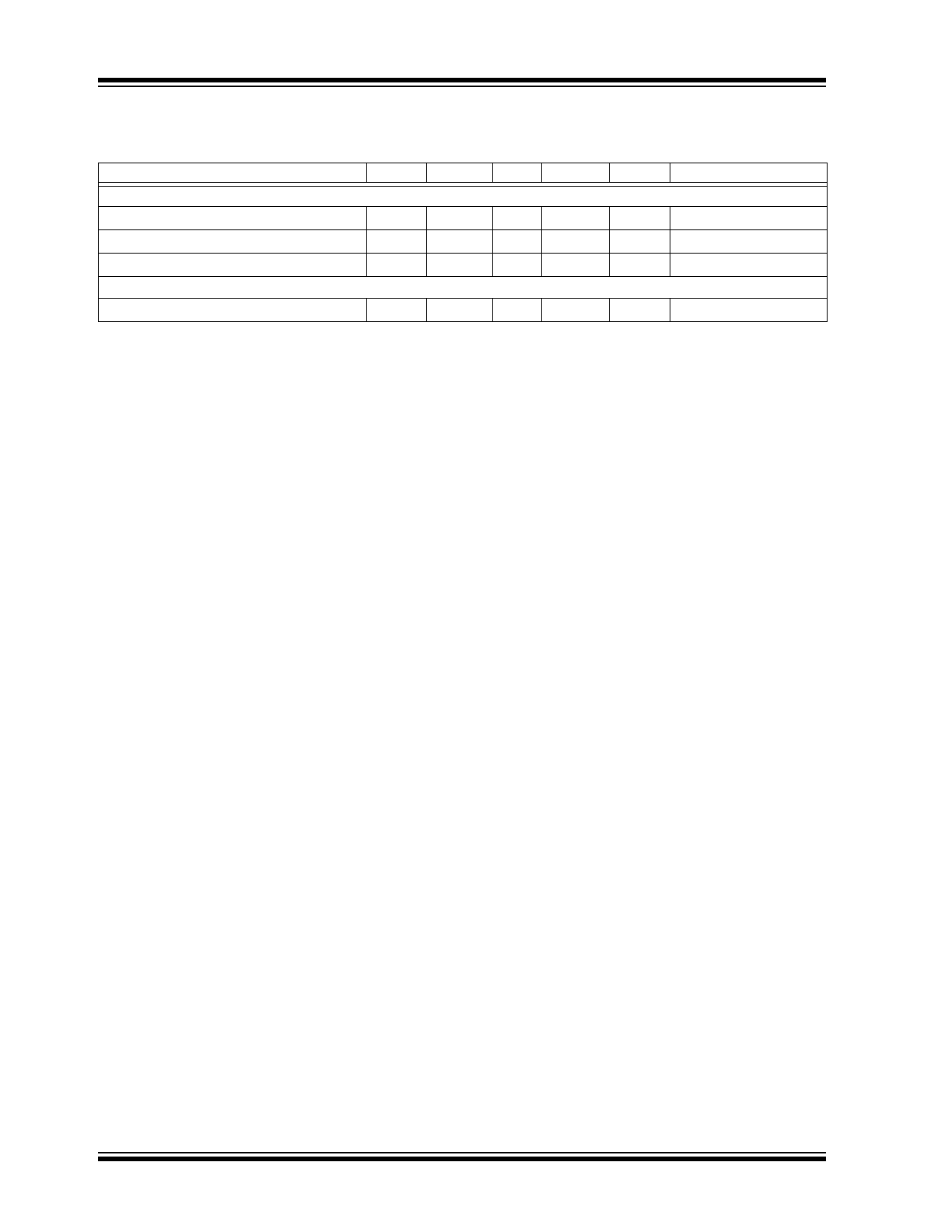
TEMPERATURE CHARACTERISTICS
Electrical Specifications:
Unless otherwise indicated, all parameters apply with 10V
V
DD
20V.
Parameters
Symbol
Min.
Typ.
Max.
Units
Conditions
Temperature Ranges
Specified Temperature Range (
Note 1
)
T
A
–40
—
+125
°C
—
Operating Temperature Range
T
A
–40
—
+125
°C
—
Storage Temperature Range
T
S
–60
—
+150
°C
—
Thermal Package Resistances
Thermal Resistance, 28LD SOICW
JA
—
53
—
°C/W
—
Note 1:
Operation in this range must not cause T
J
to exceed Maximum Junction Temperature (+125°C).
2017 Microchip Technology Inc.
DS20005531B-page 9
MIC4609
2.0
TYPICAL PERFORMANCE CURVES
Note:
Unless otherwise indicated, T
A
= +25°C with 10V
V
DD
20V.
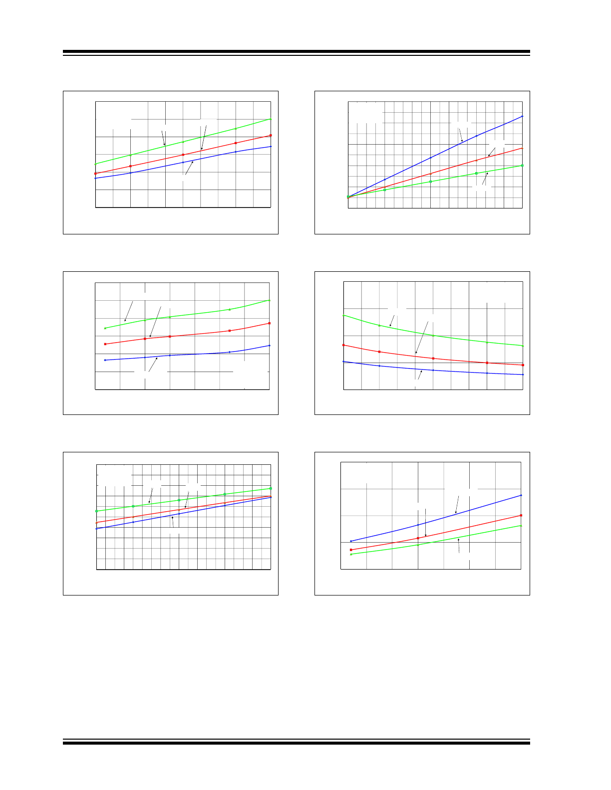
FIGURE 2-1:
V
DD
Quiescent Current vs.
V
DD
Voltage.
FIGURE 2-2:
V
DD
Quiescent Current vs.
Temperature.
FIGURE 2-3:
V
HB
Quiescent Current vs.
V
HB
Voltage.
FIGURE 2-4:
V
HB
Quiescent Current vs.
Temperature.
FIGURE 2-5:
V
DD+HB
Shutdown Current
vs. Voltage.
FIGURE 2-6:
V
DD+HB
Shutdown Current
vs. Temperature.
Note:
The graphs and tables provided following this note are a statistical summary based on a limited number of
samples and are provided for informational purposes only. The performance characteristics listed herein
are not tested or guaranteed. In some graphs or tables, the data presented may be outside the specified
operating range (e.g., outside specified power supply range) and therefore outside the warranted range.
0
20
40
60
80
100
120
140
10
11
12
13
14
15
16
17
18
19
20
V
DD
Quiescent Current
(μA)
V
DD
(V)
-40°C
25°C
125°C
V
HS
= GND
EN = V
DD
0
20
40
60
80
100
120
140
-50
-25
0
25
50
75
100
125
V
DD
Q
u
iescent Current
(μA)
Temperature (°C)
V
DD
= 20V
V
DD
= 10V
V
DD
= 15V
V
HS
= GND
EN = V
DD
0
10
20
30
40
50
10
12
14
16
18
20
V
HB
Quiescent Current (μA
)
V
HB
(V)
-40°C
25°C
125°C
V
HS
= GND
EN = V
DD
0
10
20
30
40
50
-50
-25
0
25
50
75
100
125
V
HB
Q
u
iescent Current
(μA)
Temperature (°C)
V
HB
= 20V
V
HB
= 10V
V
HB
= 14V
V
HS
= GND
EN = V
DD
0.001
0.01
0.1
1
10
10
11
12
13
14
15
16
17
18
19
20
V
DD
+H
B
Shutdow
n Current
(μA)
V
DD+HB
(V)
-40°C
25°C
125°C
HI = LI = 0V
V
HS
= Floating
EN = 0V
V
DD
= V
HB
0.0001
0.001
0.01
0.1
1
10
-50
-25
0
25
50
75
100
125
V
DD
+H
B
Shutdow
n Current
(μA)
Temperature (°C)
V
DD
= 15V
V
DD
= 10V
V
DD
= 20V
HI = LI = 0V
V
HS
= Floating
EN = 0V
V
DD
= V
HB
MIC4609
DS20005531B-page 10
2017 Microchip Technology Inc.
Note:
Unless otherwise indicated, T
A
= +25°C with 10V
V
DD
20V.
FIGURE 2-7:
V
DD+HB
Shutdown Current
vs. Voltage.
FIGURE 2-8:
V
DD+HB
Shutdown Current
vs. Temperature.
FIGURE 2-9:
V
DD
Operating Current vs.
Frequency.
FIGURE 2-10:
V
HB
Operating Current vs.
Frequency – One Phase.
FIGURE 2-11:
HO Output Sink
ON-Resistance vs. V
DD
.
FIGURE 2-12:
HO Output Sink
ON-Resistance vs. Temperature.
0
20
40
60
80
100
120
10
11
12
13
14
15
16
17
18
19
20
V
DD
+H
B
Sh
utdow
n
Current
(μA
)
V
DD+HB
(V)
HI = LI = 0V
V
HS
= GND
EN = 0V
V
DD
= V
HB
-40ºC
25ºC
125ºC
0
20
40
60
80
100
120
-50
-25
0
25
50
75
100
125
V
DD+H
B
Shutdow
n Current
(μA)
Temperature (°C)
V
DD
= 15V
V
DD
= 10V
V
DD
= 20V
HI = LI = 0V
V
HS
= GND
EN = 0V
V
DD
= V
HB
0
20
40
60
80
100
120
140
160
180
200
1 2 3 4 5 6 7 8 9 10 11 12 13 14 15 16 17 18 19 20
V
DD
O
p
er
at
ing Cur
rent
(
μ
A)
Frequency (kHz)
-40ºC
25ºC
125ºC
V
HB
= V
DD
V
HS
= 0V
C
L
= 0 nF
0
20
40
60
80
100
120
140
160
180
200
1 2 3 4 5 6 7 8 9 10 11 12 13 14 15 16 17 18 19 20
V
HB
O
p
er
at
ing Cur
rent
(
μ
A)
Frequency (kHz)
-40ºC
25ºC
125ºC
V
HB
= V
DD
V
HS
= 0V
C
L
= 0 nF
5
10
15
20
25
10
11
12
13
14
15
16
17
18
19
20
R
ON
Sink
(Ω
)
V
DD
(V)
-40ºC
25ºC
125ºC
I
HO
= 50 mA
V
HS
= GND
EN = V
HB
= V
DD
5
10
15
20
25
-50
-25
0
25
50
75
100
125
R
ON
Sink (
Ω
)
Temperature (°C)
V
DD
= 20V
V
DD
= 15V
V
DD
= 10V
I
HO
= 50 mA
V
HS
= GND
EN = V
HB
= V
DD