
2017 Microchip Technology Inc.
DS20005720A-page 1
MIC5209
Features
• Output Voltage Range: 1.8V – 15V
• Meets Intel
®
Slot 1 and Slot 2 Requirements
• Guaranteed 500 mA Output Over the Full
Operating Temperature Range
• Low 500 mV Maximum Dropout Voltage at Full
Load
• Extremely Tight Load and Line Regulation
• Thermally Efficient Surface-Mount Package
• Low Temperature Coefficient
• Current and Thermal Limiting
• Reversed-Battery Protection
• No-Load Stability
• 1% Output Accuracy
• Ultra-Low-Noise Capability in SOIC-8 and DDPAK
• Ultra-Small 3 mm × 3 mm DFN Package
Applications
• Pentium II Slot 1 and Slot 2 Support Circuits
• Laptop, Notebook, and Palmtop Computers
• Cellular Telephones
• Consumer and Personal Electronics
• SMPS Post-Regulator and DC/DC Modules
• High-Efficiency Linear Power Supplies
General Description
The MIC5209 is an efficient linear voltage regulator
with very low dropout voltage, typically 10 mV at light
loads and less than 500 mV at full load, with better than
1% output voltage accuracy.
Designed especially for hand-held, battery-powered
devices, the MIC5209 features low ground current to
help prolong battery life. An enable/shutdown pin on
the SOIC-8 and DDPAK versions can further improve
battery life with near-zero shutdown current.
Key features include reversed-battery protection,
current limiting, overtemperature shutdown,
ultra-low-noise capability (SOIC-8 and DDPAK
versions), and is available in thermally efficient
packaging. The MIC5209 is available in adjustable or
fixed output voltages.
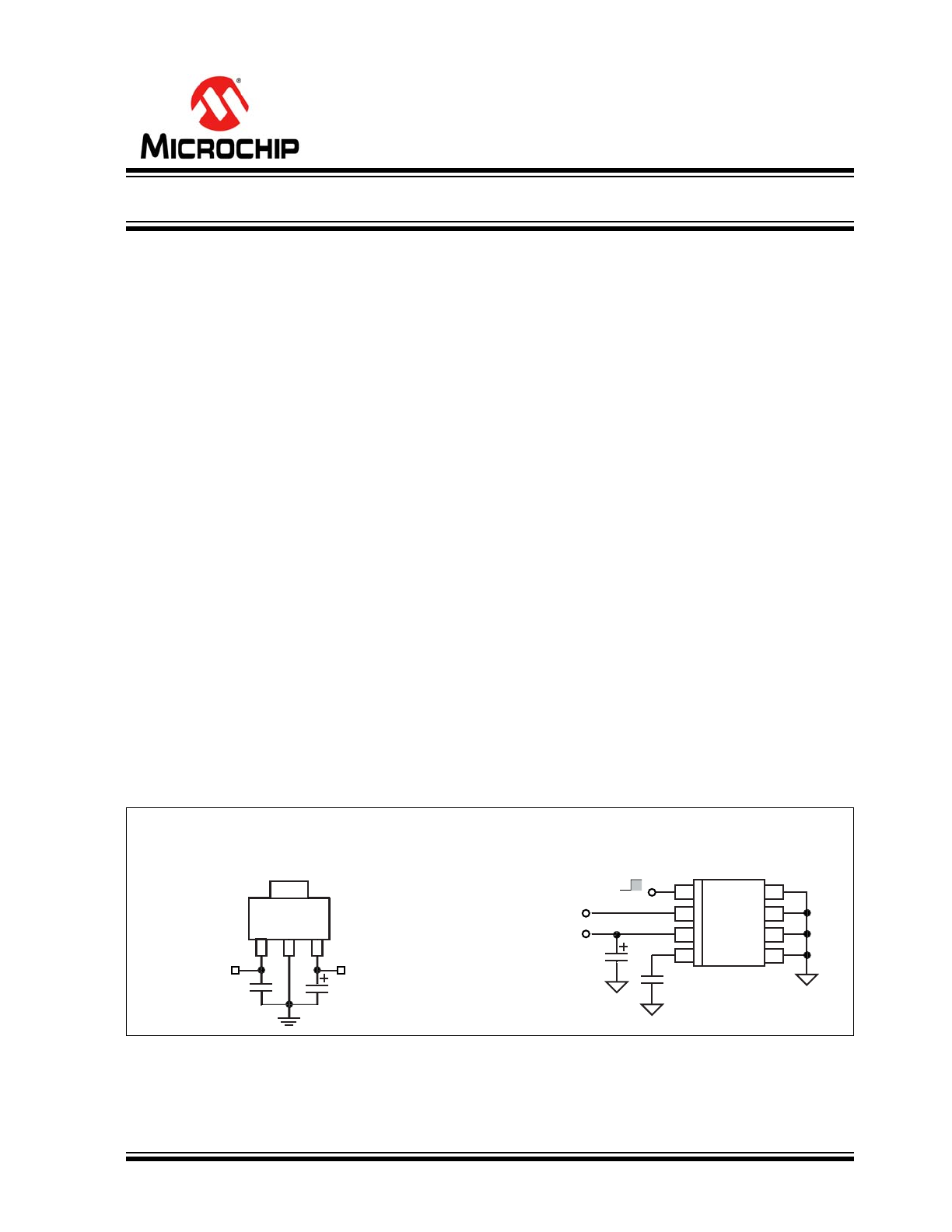
Typical Application Circuits
3.3V N
OMINAL
I
NPUT
S
LOT
1
P
OWER
S
UPPLY
U
LTRA
-L
OW
N
OISE
5V R
EGULATOR
MIC5209-2.5YS
V
IN
3.0V
0.1μF
V
OUT
2.5V ±1%
22μF
TANTALUM
1
2
3
MIC5209-5.0YM
V
IN
6.0V
V
OUT
5.0V
22μF
TANTALUM
1
2
3
4
5
6
7
8
ENABLE
SHUTDOWN
470pF
(OPTIONAL)
500 mA Low-Noise LDO Regulator
MIC5209
DS20005720A-page 2
2017 Microchip Technology Inc.
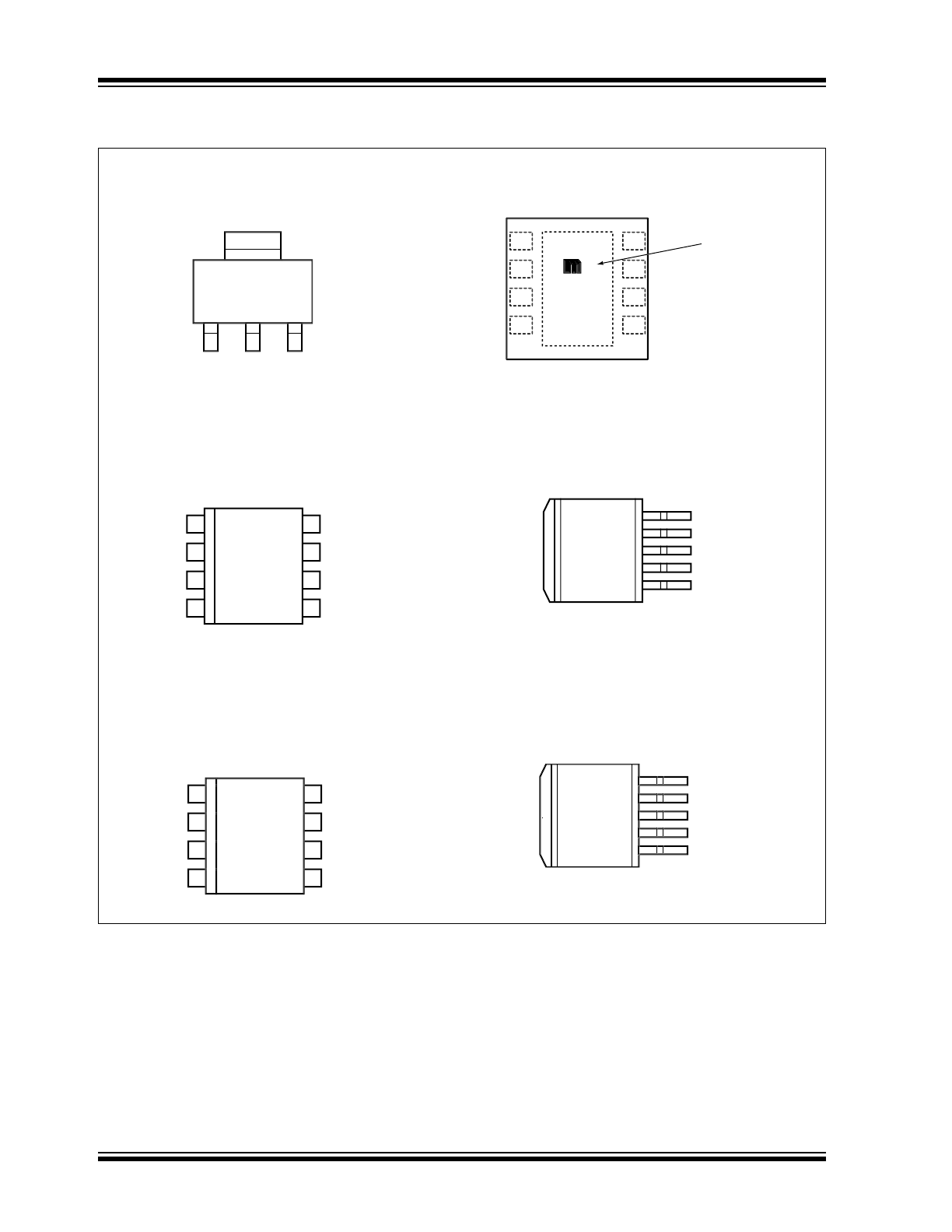
Package Types
MIC5209-
X
.
X
YS
SOT-223 (S)
F
IXED
V
OLTAGES
(T
OP
V
IEW
)
MIC5209YML
8-P
IN
3
X
3 DFN (ML)
A
DJUSTABLE
V
OLTAGES
(T
OP
V
IEW
)
1
IN
IN
OUT
OUT
8
EN
GND
ADJ
NC
7
6
5
2
3
4
5209
YWW
Y
PART
IDENTIFICATION
EP
IN
OUT
GND
1
3
2
TAB
GND
MIC5209-
X
.
X
YM
SOIC-8 (M)
F
IXED
V
OLTAGES
(T
OP
V
IEW
)
1
2
3
4
8
7
6
5
GND
GND
GND
GND
EN
IN
OUT
BYP
MIC5209-
X
.
X
YU
DDPAK (U)
F
IXED
V
OLTAGES
(T
OP
V
IEW
)
5 BYP
4 OUT
3 GND
2 IN
1 EN
D
N
G
B
A
T
MIC5209YM
SOIC-8 (M)
A
DJUSTABLE
V
OLTAGES
(T
OP
V
IEW
)
MIC5209YU
DDPAK (U)
A
DJUSTABLE
V
OLTAGES
(T
OP
V
IEW
)
1
2
3
4
8
7
6
5
GND
GND
GND
GND
EN
N
IN
OUT
OUT
J
ADJ
5 ADJ
4 OUT
3 GND
2 IN
1 EN
D
N
G
B
A
T
AA
2017 Microchip Technology Inc.
DS20005720A-page 3
MIC5209
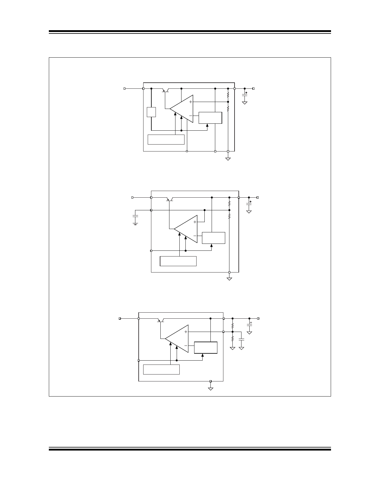
Functional Diagrams
L
OW
-N
OISE
F
IXED
R
EGULATOR
(SOT-223 V
ERSION
O
NLY
)
U
LTRA
-L
OW
-N
OISE
F
IXED
R
EGULATOR
V
IN
IN
MIC5209-x.xYS
OUT
V
OUT
C
OUT
GND
~2.0V – 2.1V
–40ºC
BANDGAP
REFERENCE
EN
CURRENT-LIMIT
THERMAL SHUTDOWN
V
IN
IN
MIC5209-x.xYM/U
OUT
V
OUT
C
OUT
GND
BANDGAP
REFERENCE
EN
CURRENT-LIMIT
THERMAL SHUTDOWN
C
BYP
(OPTIONAL)
BYP
U
LTRA
-L
OW
-N
OISE
A
DJUSTABLE
R
EGULATOR
V
IN
IN
MIC5209YM/U (ADJUSTABLE)
OUT
V
OUT
C
OUT
GND
BANDGAP
REFERENCE
EN
CURRENT-LIMIT
THERMAL SHUTDOWN
C
BYP
(OPTIONAL)
ADJ
R1
R2

MIC5209
DS20005720A-page 4
2017 Microchip Technology Inc.
1.0
ELECTRICAL CHARACTERISTICS
Absolute Maximum Ratings †
Supply Voltage (V
IN
).................................................................................................................................... –20V to +20V
Power Dissipation (P
D
) (
Note 1
).............................................................................................................Internally Limited
ESD Rating (SOT-223)..................................................................................................................... 2 kV HBM/300V MM
ESD Rating (DFN, SOIC-8).............................................................................................................. 5 kV HBM/100V MM
Operating Ratings ‡
Supply Voltage (V
IN
)................................................................................................................................... +2.5V to +16V
Adjustable Output Voltage Range (V
OUT
) .................................................................................................. +1.8V to +15V
† Notice: Stresses above those listed under “Absolute Maximum Ratings” may cause permanent damage to the device.
This is a stress rating only and functional operation of the device at those or any other conditions above those indicated
in the operational sections of this specification is not intended. Exposure to maximum rating conditions for extended
periods may affect device reliability.
‡ Notice: The device is not guaranteed to function outside its operating ratings.
Note 1: The maximum allowable power dissipation at any T
A
(ambient temperature) is P
D(max)
= (T
J(max)
– T
A
) x θ
JA
.
Exceeding the maximum allowable power dissipation will cause excessive die temperature, and the regula-
tor will go into thermal shutdown. See
Table 4-1
and the
Thermal Considerations
sub-section in
Applications
Information
for details.
2017 Microchip Technology Inc.
DS20005720A-page 5
MIC5209
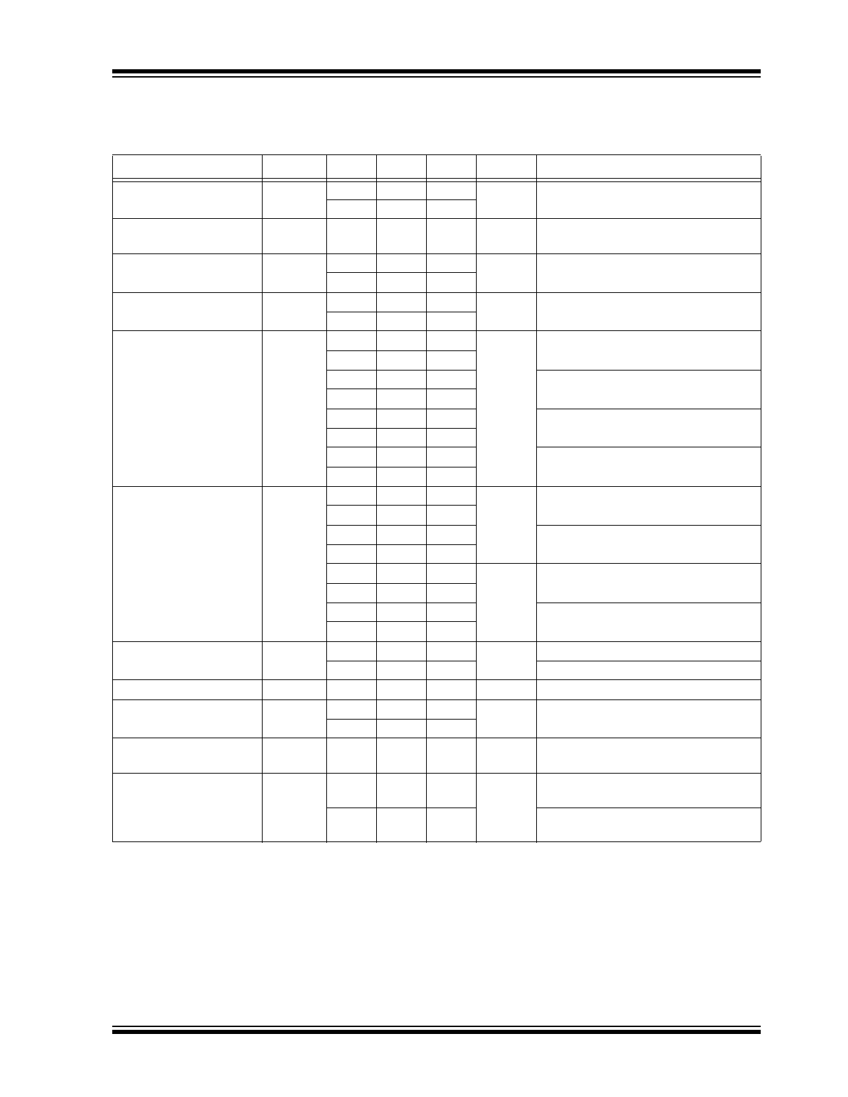
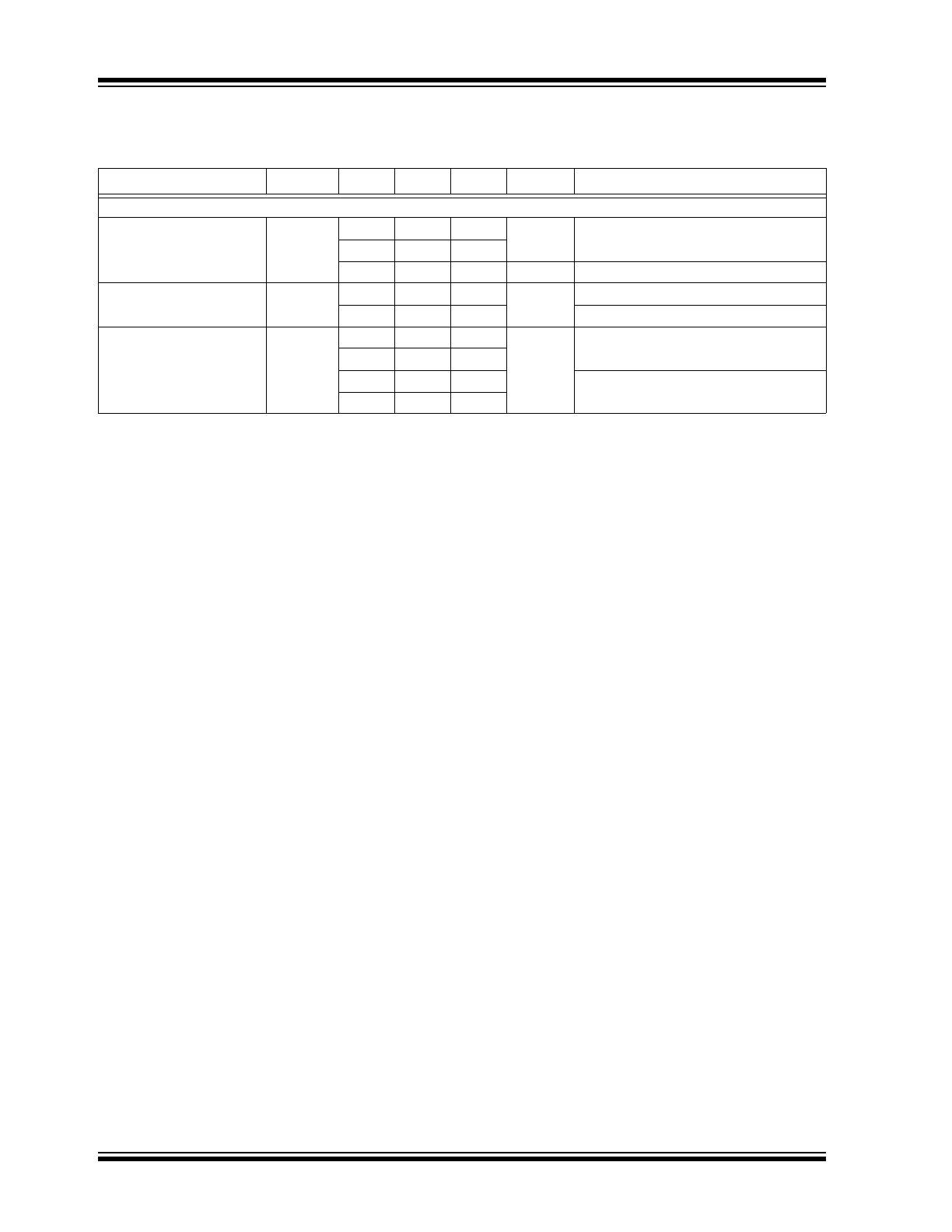
TABLE 1-1:
ELECTRICAL CHARACTERISTICS (
Note 1
)
Electrical Characteristics: V
IN
= V
OUT
+ 1V; I
L
= 100 μA; T
J
= +25°C, bold values indicate –40°C ≤ T
J
≤ +125°C
except 0°C ≤ T
J
≤ +125°C for 1.8V ≤ V
OUT
≤ 2.5V, unless noted.
Parameter
Symbol
Min.
Typ.
Max.
Units
Conditions
Output Voltage Accuracy
V
OUT
–1
—
1
%
Variation from nominal V
OUT
–2
—
2
Output Voltage
Temperature Coefficient
∆V
OUT
/
∆T
—
40
—
ppm/°C
Note 2
Line Regulation
∆V
OUT
/
V
OUT
—
0.009
0.05
%
V
IN
= V
OUT
+ 1V to 16V
—
—
0.10
Load Regulation
∆V
OUT
/
V
OUT
—
0.05
0.5
%
I
L
= 100 µA to 500 mA,
Note 3
—
—
0.7
Dropout Voltage, (
Note 4
)
V
IN
–
V
OUT
—
10
60
mV
I
L
= 100 µA
—
—
80
—
115
175
I
L
= 50 mA
—
—
250
—
165
300
I
L
= 150 mA
—
—
400
—
350
500
I
L
= 500 mA
—
—
600
Ground Pin Current
(
Note 5
,
Note 6
)
I
GND
—
80
130
µA
V
EN
≥ 3.0V, I
OUT
= 100 µA
—
—
170
—
350
650
V
EN
≥ 3.0V, I
OUT
= 50 mA
—
—
900
—
1.8
2.5
mA
V
EN
≥ 3.0V, I
OUT
= 150 mA
—
—
3.0
—
8
20
V
EN
≥ 3.0V, I
OUT
= 500 mA
—
—
25
Ground Pin Quiescent
Current, (
Note 6
)
I
GND
—
0.05
3
µA
V
EN
≤ 0.4V (shutdown)
—
0.10
8
V
EN
≤ 0.18V (shutdown)
Ripple Rejection
PSRR
—
75
—
dB
f = 120 Hz
Current Limit
I
LIMIT
—
700
900
mA
V
OUT
= 0V
—
—
1000
Thermal Regulation
∆V
OUT
/
∆P
D
—
0.05
—
%/W
Note 7
Output Noise, (
Note 8
)
e
n
—
500
—
nV √Hz
V
OUT
= 2.5V, I
OUT
= 50 mA
C
OUT
= 2.2 µF, C
BYP
= 0
—
300
—
I
OUT
= 50 mA, C
OUT
= 2.2 µF
C
BYP
= 470 pF
MIC5209
DS20005720A-page 6
2017 Microchip Technology Inc.
Enable Input
Enable Input Logic-Low
Voltage
V
ENL
—
—
0.4
V
V
EN
= Logic-low (Regulator shutdown)
—
—
0.18
2.0
—
—
V
V
EN
= Logic-high (Regulator enabled)
Enable Input Current
I
ENL
—
0.01
–1
µA
V
ENL
≤ 0.4V
—
0.01
–2
V
ENL
≤ 0.18V
—
I
ENH
—
5
20
µA
V
ENH
≥ 2.0V
—
—
25
—
—
30
V
ENH
≥ 16V
—
—
50
Note 1: Specification for packaged product only.
2: Output voltage temperature coefficient is defined as the worst-case voltage change divided by the total
temperature range.
3: Regulation is measured at constant junction temperature using low duty cycle pulse testing. Parts are
tested for load regulation in the load range from 100 µA to 500 mA. Changes in output voltage due to heat-
ing effects are covered by the thermal regulation specification.
4: Dropout Voltage is defined as the input to output differential at which the output voltage drops 2% below its
nominal value measured at 1V differential.
5: Ground pin current is the regulator quiescent current plus pass transistor base current. The total current
drawn from the supply is the sum of the load current plus the ground pin current.
6: V
EN
is the voltage externally applied to devices with the EN (enable) input pin. SOIC-8 (M) and DDPAK (U)
packages only.
7: Thermal regulation is the change in output voltage at a time “t” after a change in power dissipation is
applied, excluding load or line regulation effects. Specifications are for a 500 mA load pulse at V
IN
= 16V
for t = 10 ms.
8: C
BYP
is an optional, external bypass capacitor connected to devices with a BYP (bypass) or ADJ (adjust)
pin. SOIC-8 (M) and DDPAK (U) packages only.
TABLE 1-1:
ELECTRICAL CHARACTERISTICS (
Note 1
) (CONTINUED)
Electrical Characteristics: V
IN
= V
OUT
+ 1V; I
L
= 100 μA; T
J
= +25°C, bold values indicate –40°C ≤ T
J
≤ +125°C
except 0°C ≤ T
J
≤ +125°C for 1.8V ≤ V
OUT
≤ 2.5V, unless noted.
Parameter
Symbol
Min.
Typ.
Max.
Units
Conditions
2017 Microchip Technology Inc.
DS20005720A-page 7
MIC5209
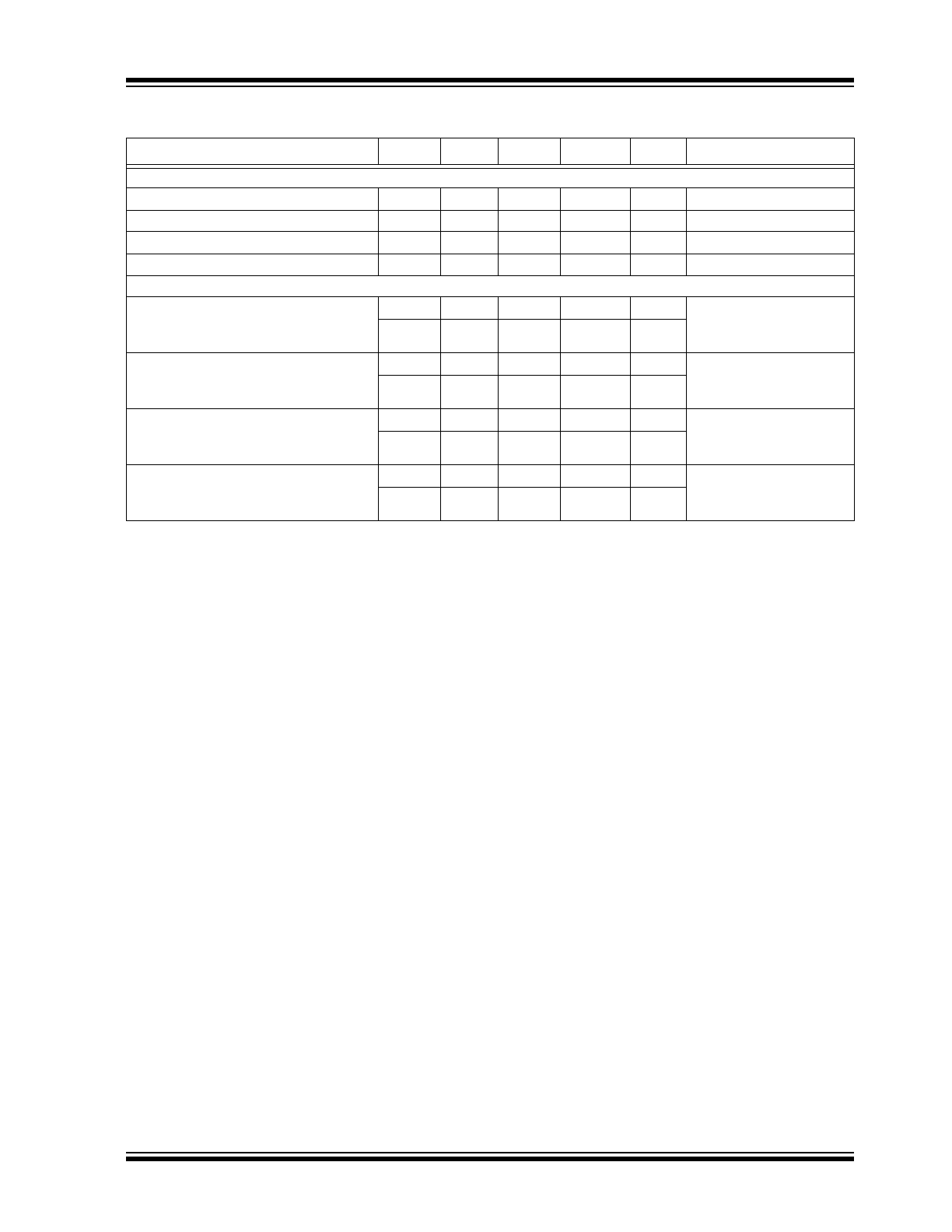
TEMPERATURE SPECIFICATIONS (
Note 1
)
Parameters
Sym.
Min.
Typ.
Max.
Units
Conditions
Temperature Ranges
Storage Temperature Range
T
S
–65
—
+150
°C
—
Lead Temperature
—
—
—
+260
°C
Soldering, 5 sec.
Junction Temperature
T
J
–40
—
+125
°C
2.5V ≤ V
OUT
≤ 15V
Junction Temperature
T
J
0
—
+125
°C
1.8V ≤ V
OUT
< 2.5V
Package Thermal Resistance
Thermal Resistance SOT-223
θ
JA
—
62
—
°C/W
EIA/JEDEC
JES51-751-7,
4 Layer Board
θ
JC
—
15
—
°C/W
Thermal Resistance SOIC-8
θ
JA
—
50
—
°C/W
See
Thermal
Considerations
for more
information.
θ
JC
—
25
—
°C/W
Thermal Resistance DDPAK
θ
JA
—
31.4
—
°C/W
EIA/JEDEC
JES51-751-7,
4 Layer Board
θ
JC
—
3
—
°C/W
Thermal Resistance 3 mm x 3 mm
DFN
θ
JA
—
64
—
°C/W
EIA/JEDEC
JES51-751-7,
4 Layer Board
θ
JC
—
12
—
°C/W
Note 1: The maximum allowable power dissipation is a function of ambient temperature, the maximum allowable
junction temperature and the thermal resistance from junction to air (i.e., T
A
, T
J
,
JA
). Exceeding the
maximum allowable power dissipation will cause the device operating junction temperature to exceed the
maximum +125°C rating. Sustained junction temperatures above +125°C can impact the device reliability.
MIC5209
DS20005720A-page 8
2017 Microchip Technology Inc.
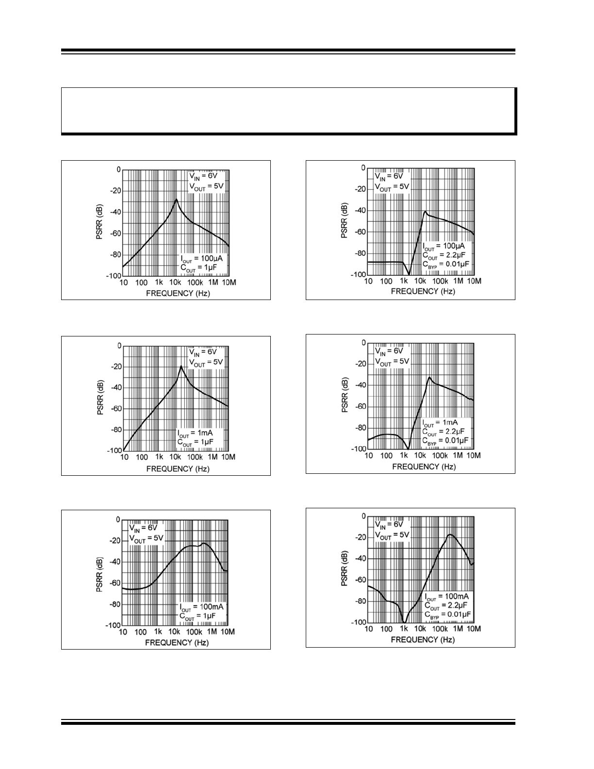
2.0
TYPICAL PERFORMANCE CURVES
FIGURE 2-1:
Power Supply Rejection
Ratio.
FIGURE 2-2:
Power Supply Rejection
Ratio.
FIGURE 2-3:
Power Supply Rejection
Ratio.
FIGURE 2-4:
Power Supply Rejection
Ratio.
FIGURE 2-5:
Power Supply Rejection
Ratio.
FIGURE 2-6:
Power Supply Rejection
Ratio.
Note:
The graphs and tables provided following this note are a statistical summary based on a limited number of
samples and are provided for informational purposes only. The performance characteristics listed herein
are not tested or guaranteed. In some graphs or tables, the data presented may be outside the specified
operating range (e.g., outside specified power supply range) and therefore outside the warranted range.
2017 Microchip Technology Inc.
DS20005720A-page 9
MIC5209
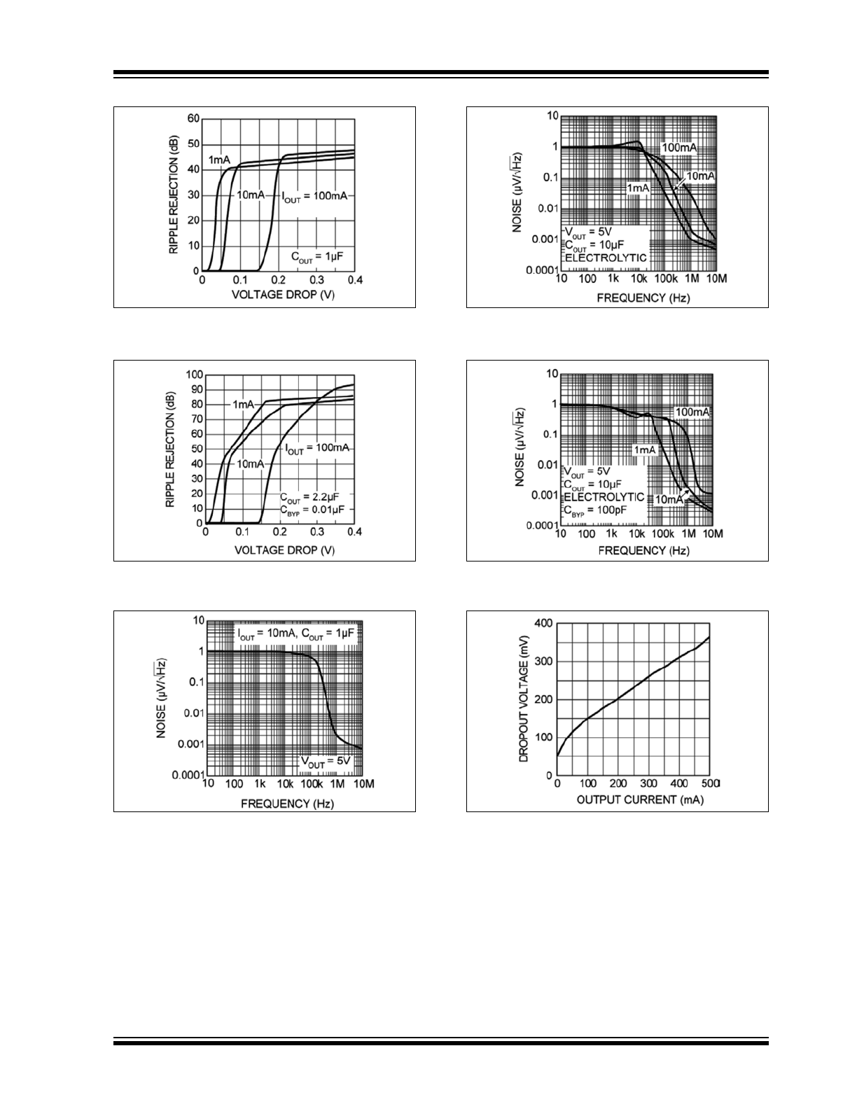
FIGURE 2-7:
Power Supply Ripple
Rejection vs. Voltage Drop.
FIGURE 2-8:
Power Supply Ripple
Rejection vs. Voltage Drop.
FIGURE 2-9:
Noise Performance.
FIGURE 2-10:
Noise Performance.
FIGURE 2-11:
Noise Performance.
FIGURE 2-12:
Dropout Voltage vs. Output
Current.
MIC5209
DS20005720A-page 10
2017 Microchip Technology Inc.
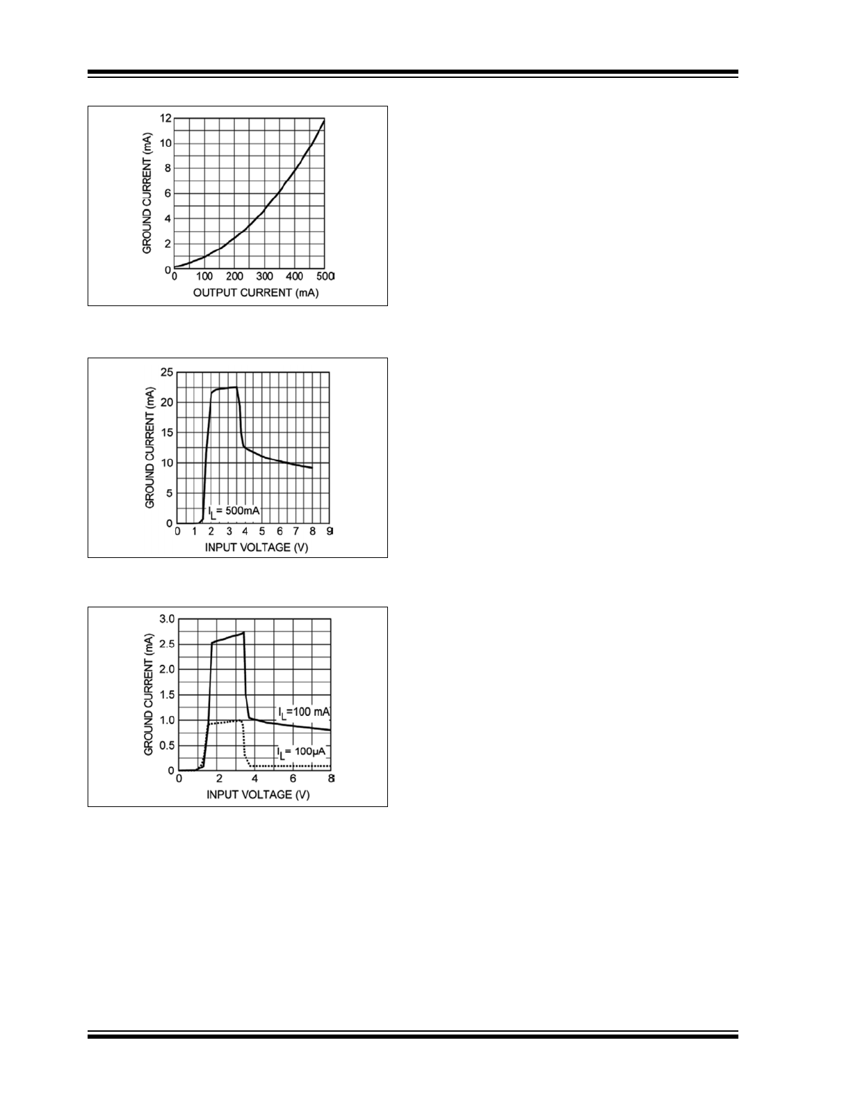
FIGURE 2-13:
Ground Current vs. Output
Current.
FIGURE 2-14:
Ground Current vs. Supply
Voltage.
FIGURE 2-15:
Ground Current vs. Supply
Voltage.