
2002 Microchip Technology Inc.
DS21379B-page 1
TC1268
Features
• Very Low Dropout Voltage
• 500mA Output Current
• High Output Voltage Accuracy
• Standard or Custom Output Voltages
• Over Current and Over Temperature Protection
• SHDN Input for Active Power Management
• ERROR Output to Detect Low Battery
• 5
µ
sec (typical) Wake-up Time from SHDN
Applications
• RAMBUS Memory Module
• Battery-Operated Systems
• Portable Computers
• Medical Instruments
• Instrumentation
• Cellular/GSM/PHS Phones
• Linear Post-Regulator for SMPS
• Pagers
• Digital Cameras
Device Selection Table
*Other output voltages and package options are available.
Please contact Microchip Technology Inc. for details.
Package Type
General Description
The TC1268 is a fixed output, fast turn-on, high
accuracy
(typically
±0.5%)
CMOS
low
dropout
regulator. Designed specifically for battery-operated
systems, the TC1268’s CMOS construction eliminates
wasted ground current, significantly extending battery
life. Total supply current is typically 80
µ
A at full load (20
to 60 times lower than in bipolar regulators).
TC1268’s key features include ultra low noise, very low
dropout voltage (typically 350mV at full load), and
fast response to step changes in load. The TC1268
also has a fast wake-up response time (5
µ
sec typically)
when
released
from
shutdown.
The
TC1268
incorporates both over temperature and over current
protection. The TC1268 is stable with an output
capacitor of only 1
µ
F and has a maximum output
current of 500mA.
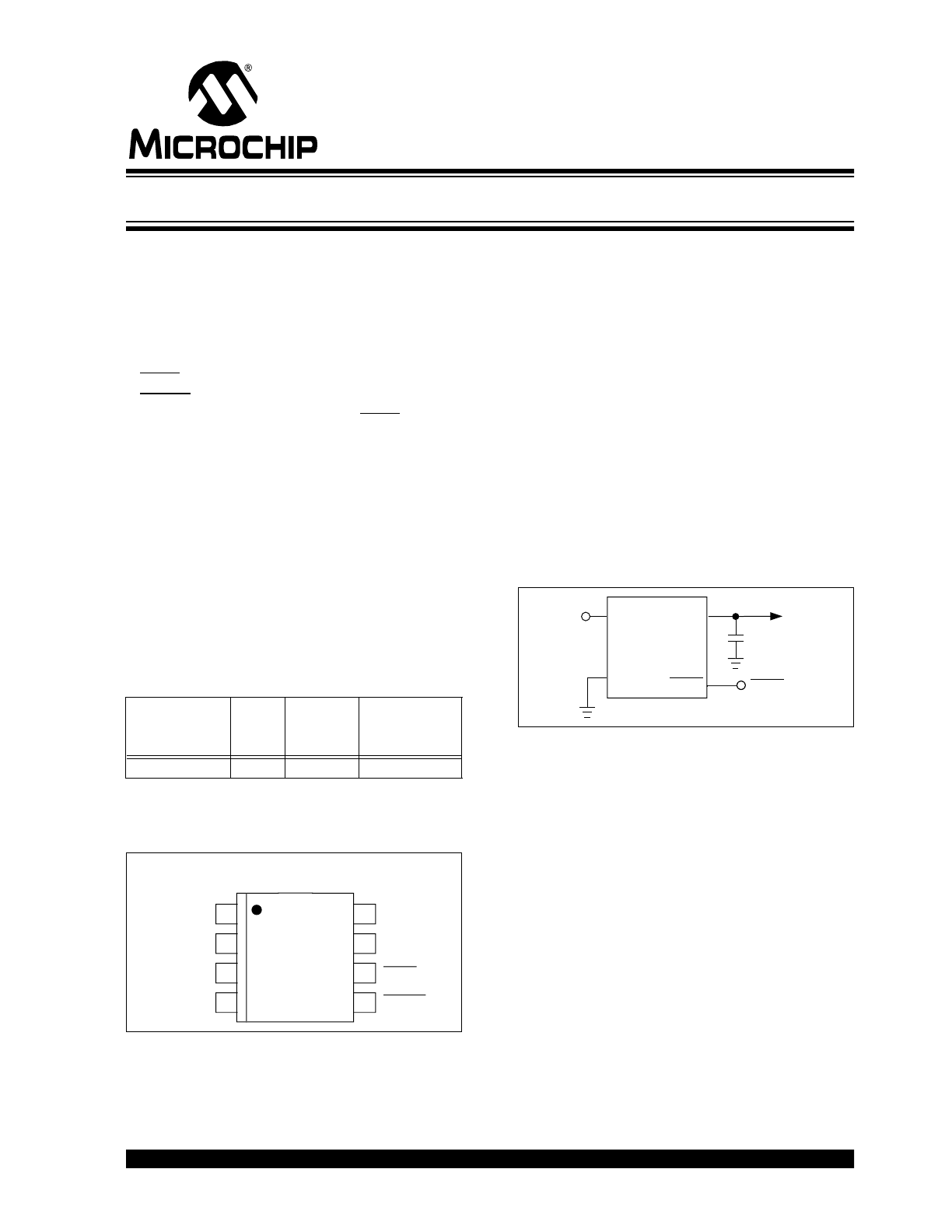
Typical Application
Part Number
Output*
Voltage
(V)
Package
Junction
Temp. Range
TC1268-2.5VOA
2.5
8-Pin SOIC -40°C to +125°C
1
2
3
4
8
7
6
5
TC1268
NC
SHDN
8-Pin SOIC
GND
NC
BYPASS
V
OUT
V
IN
ERROR
TC1268
V
IN
V
OUT
C
OUT
1
µF
GND
V
OUT
V
IN
SHDN
SHDN
+
500mA Fixed Output, Fast Response CMOS LDO with Shutdown
TC1268
DS21379B-page 2
2002 Microchip Technology Inc.
1.0
ELECTRICAL
CHARACTERISTICS
Absolute Maximum Ratings*
Input Voltage .........................................................6.5V
Power Dissipation................Internally Limited (Note 6)
Maximum Voltage on Any Pin ........ V
IN
+0.3V to -0.3V
Operating Temperature ............... -40°C < T
J
< +125°C
Storage Temperature.......................... -65°C to +150°C
*Stresses above those listed under "Absolute Maximum
Ratings" may cause permanent damage to the device. These
are stress ratings only and functional operation of the device
at these or any other conditions above those indicated in the
operation sections of the specifications is not implied.
Exposure to Absolute Maximum Rating conditions for
extended periods may affect device reliability.
TC1268 ELECTRICAL SPECIFICATIONS
Electrical Characteristics: V
IN
= V
OUT
+ 1V, I
L
= 100
µ
A, C
L
= 3.3
µ
F, SHDN > V
IH
, T
A
= 25°C, unless otherwise noted. Boldface
type specifications apply for junction temperatures of -40°C to +125°C.
Symbol
Parameter
Min
Typ
Max
Units
Test Conditions
V
IN
Input Operating Voltage
2.7
—
6.0
V
Note 8
I
OUT
MAX
Maximum Output Current
500
—
—
mA
V
OUT
Output Voltage
—
V
R
– 2.5%
V
R
±0.5%
—
—
V
R
+ 2.5%
V
Note 1
∆
V
OUT
/
∆
T
V
OUT
Temperature Coefficient
—
40
—
ppm/°C
Note 2
∆
V
OUT
/
∆
V
IN
Line Regulation
—
0.05
0.35
%
(V
R
+ 1V)
≤
V
IN
≤
6V
∆
V
OUT
/V
OUT
Load Regulation
—
0.002
0.01
%/mA
I
L
= 0.1mA to I
OUT
MAX
(Note 3)
V
IN
-V
OUT
Dropout Voltage
—
—
—
—
20
60
200
350
30
160
480
800
mV
I
L
= 100
µ
A
I
L
= 100mA
I
L
= 300mA
I
L
= 500mA (Note 4)
I
DD
Supply Current (Active Mode)
—
80
130
µ
A
SHDN = V
IH
, I
L
= 0
I
SHDN
Supply Current (Shutdown Mode)
—
5
—
µ
A
SHDN = 0V
T
WK
Wake-up Time
(from Shutdown Mode)
—
5
10
µ
sec
V
IN
= 3.5V, V
OUT
= 2.5V
C
IN
= C
OUT
= 1
µ
F
I
L
= 250mA (See Figure 3-2)
T
S
Settling Time
(from Shutdown Mode)
—
15
—
µ
sec
V
IN
= 3.5V, V
OUT
= 2.5V
C
IN
= C
OUT
= 1
µ
F
I
L
= 250mA (See Figure 3-2)
PSRR
Power Supply Rejection Ratio
—
64
—
dB
F
RE
≤
1kHz
I
OUT
SC
Output Short Circuit Current
—
1200
1400
mA
V
OUT
= 0V
∆
V
OUT
/
∆
P
D
Thermal Regulation
—
0.04
—
V/W
Note 5
eN
Output Noise
—
260
—
nV/
√
Hz
I
L
= I
OUT
MAX
SHDN Input
V
IH
SHDN Input High Threshold
45
—
—
%V
IN
V
IL
SHDN Input Low Threshold
—
—
15
%V
IN
Note 1:
V
R
is the regulator output voltage setting.
2:
3:
Regulation is measured at a constant junction temperature using low duty cycle pulse testing. Load regulation is tested over a load range from
0.1mA to the maximum specified output current. Changes in output voltage due to heating effects are covered by the thermal regulation
specification.
4:
Dropout voltage is defined as the input to output differential at which the output voltage drops 2% below its nominal value measured at a 1V
differential.
5:
Thermal Regulation is defined as the change in output voltage at a time T after a change in power dissipation is applied, excluding load or
line regulation effects. Specifications are for a current pulse equal to I
L
MAX
at V
IN
= 6V for T = 10 msec.
6:
The maximum allowable power dissipation is a function of ambient temperature, the maximum allowable junction temperature and the
thermal resistance from junction-to-air (i.e., T
A
, T
J
,
θ
JA
). Exceeding the maximum allowable power dissipation causes the device to initiate
thermal shutdown. Please see Section 4.0 Thermal Considerations for more details.
7:
Hysteresis voltage is referenced to V
R
.
8:
The minimum V
IN
has to justify the conditions: V
IN
≥
V
R
+ V
DROPOUT
and V
IN
≥
2.7V for I
L
= 0.1mA to I
OUT
MAX
.
T
C
V
OUT
= (V
OUT
MAX
– V
OUT
MIN
) x 10
6
V
OUT
x
∆
T
2002 Microchip Technology Inc.
DS21379B-page 3
TC1268
TC1268 ELECTRICAL SPECIFICATIONS
(CONTINUED)
Electrical Characteristics: V
IN
= V
OUT
+ 1V, I
L
= 100
µ
A, C
L
= 3.3
µ
F, SHDN > V
IH
, T
A
= 25°C, unless otherwise noted. Boldface
type specifications apply for junction temperatures of -40°C to +125°C.
ERROR Output
V
MIN
Minimum Operating Voltage
1.0
—
—
V
V
OL
Output Logic Low Voltage
—
—
400
mV
1 mA Flows to ERROR
V
TH
ERROR Threshold Voltage
—
0.95 x V
R
—
V
Note 1:
V
R
is the regulator output voltage setting.
2:
3:
Regulation is measured at a constant junction temperature using low duty cycle pulse testing. Load regulation is tested over a load range from
0.1mA to the maximum specified output current. Changes in output voltage due to heating effects are covered by the thermal regulation
specification.
4:
Dropout voltage is defined as the input to output differential at which the output voltage drops 2% below its nominal value measured at a 1V
differential.
5:
Thermal Regulation is defined as the change in output voltage at a time T after a change in power dissipation is applied, excluding load or
line regulation effects. Specifications are for a current pulse equal to I
L
MAX
at V
IN
= 6V for T = 10 msec.
6:
The maximum allowable power dissipation is a function of ambient temperature, the maximum allowable junction temperature and the
thermal resistance from junction-to-air (i.e., T
A
, T
J
,
θ
JA
). Exceeding the maximum allowable power dissipation causes the device to initiate
thermal shutdown. Please see Section 4.0 Thermal Considerations for more details.
7:
Hysteresis voltage is referenced to V
R
.
8:
The minimum V
IN
has to justify the conditions: V
IN
≥
V
R
+ V
DROPOUT
and V
IN
≥
2.7V for I
L
= 0.1mA to I
OUT
MAX
.
T
C
V
OUT
= (V
OUT
MAX
– V
OUT
MIN
) x 10
6
V
OUT
x
∆
T
TC1268
DS21379B-page 4
2002 Microchip Technology Inc.
2.0
PIN DESCRIPTIONS
The descriptions of the pins are listed in Table 2-1.
TABLE 2-1:
PIN FUNCTION TABLE
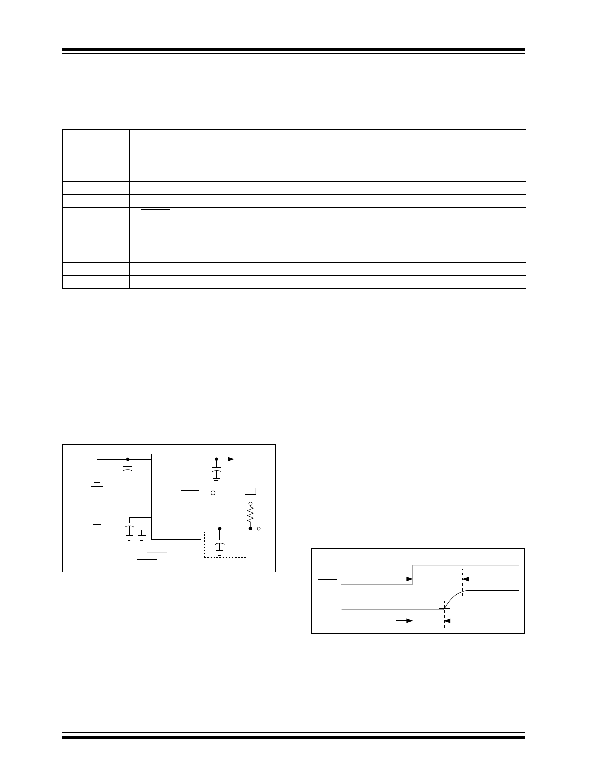
3.0
DETAILED DESCRIPTION
The TC1268 is a precision, fixed output LDO. Unlike
bipolar regulators, the TC1268 supply current does
not increase with load current. In addition, V
OUT
remains stable and within regulation over the entire
0mA to I
LOAD
MAX
load current range, (an important
consideration in RTC and CMOS RAM battery back-up
applications). Figure 3-1 shows a typical application
circuit.
FIGURE 3-1:
TYPICAL APPLICATION
CIRCUIT
3.1
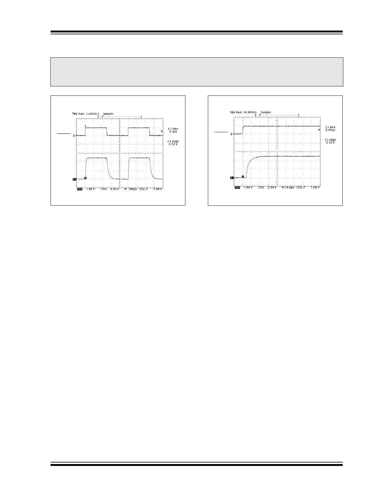
Turn On Response
The turn on response is defined as two separate
response categories, Wake-up Time (T
WK
) and Settling
Time (T
S
).
The TC1268 has a fast Wake-up Time (5
µ
sec typical)
when released from shutdown. See Figure 3-2 for the
Wake-up Time designated as T
WK
. The Wake-up Time
is defined as the time it takes for the output to rise to 2%
of the V
OUT
value after being released from shutdown.
The total turn on response is defined as the Settling
Time (T
S
), see Figure 3-2. Settling Time (inclusive with
T
WK
) is defined as the condition when the output is
within 2% of its fully enabled value (15
µ
sec typical)
when released from shutdown. The settling time of the
output voltage is dependent on load conditions and
output capacitance on V
OUT
(RC response).
The Wake-up Time (T
WK
) is an important parameter
to consider when using the TC1268 in RAMBUS
applications. In this application, the bus voltage is held
at 2.5V by a switching regulator during normal power
conditions and can be switched to low power mode,
where the TC1268 takes over and supplies the same
2.5V, but at a much lower current (300mA). In order to
not see the bus voltage drop during the transition from
high power to low power, the TC1268 has a very fast
wake-up time of 5
µ
sec to support the 2.5V rail. This
makes the TC1268 ideal for applications involving
RAMBUS.
FIGURE 3-2:
WAKE-UP RESPONSE
TIME
Pin No.
(8-Pin SOIC)
Symbol
Description
1
V
OUT
Regulated voltage output.
2
GND
Ground terminal.
3
NC
No connect.
4
BYPASS
Reference bypass input. Connecting a 470pF to this input further reduces output noise.
5
ERROR
Out-of-Regulation Flag. (Open drain output). This output goes low when V
OUT
is out-of-tolerance
by approximately -5%.
6
SHDN
Shutdown control input. The regulator is fully enabled when a logic high is applied to this input.
The regulator enters shutdown when a logic low is applied to this input. During shutdown, output
voltage falls to zero and supply current is reduced to 5
µ
A (typical).
7
NC
No connect.
8
V
IN
Unregulated supply input.
C
IN
1
µF
Battery
TC1268
V
IN
V
OUT
V
+
C1
C
OUT
1
µF
C
BYP
10nF
GND
BYP
SHDN
OFF
ON
C1 required only if ERROR is used
as a processor RESET signal (See Text)
V
OUT
0.2
µF
R1
1M
SHDN
ERROR
+
+
+
+
–
V
IH
T
S
T
WK
V
OUT
98%
2%
V
IL
SHDN
2002 Microchip Technology Inc.
DS21379B-page 5
TC1268
3.2
Bypass Input
A 10nF capacitor connected from the bypass input to
ground
reduces
noise
present
on
the
internal
reference, which in turn, significantly reduces output
noise. If output noise is not a concern, this input may be
left unconnected. Larger capacitor values may be
used, but this results in a longer time period to achieve
the rated output voltage, once power is initially applied.
3.3
Output Capacitor
A 1
µ
F (min) capacitor from V
OUT
to ground is required.
The output capacitor should have an effective series
resistance greater than 0.1
Ω
and less than 5
Ω
, and a
resonant frequency above 1MHz. A 1
µ
F capacitor
should be connected from V
IN
to GND if there is more
than 10 inches of wire between the regulator and the
AC filter capacitor, or if a battery is used as the power
source. Aluminum electrolytic or tantalum capacitor
types can be used. (Since many aluminum electrolytic
capacitors
freeze
at
approximately
-30°C,
solid
tantalums are recommended for applications operating
below -25°C.) When operating from sources other than
batteries,
supply
noise
rejection
and
transient
response can be improved by increasing the value of
the input and output capacitors and employing passive
filtering techniques.
3.4
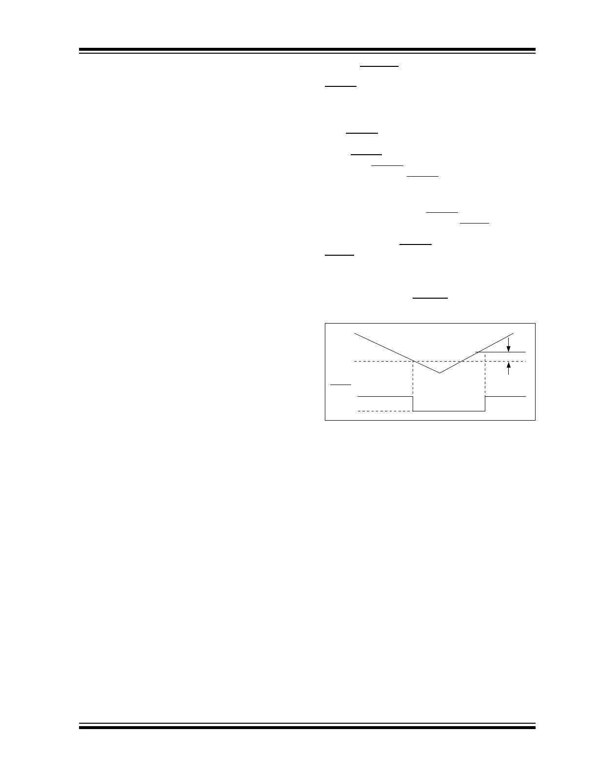
ERROR Output
ERROR is driven low whenever V
OUT
falls out of
regulation by more than -5% (typical). This condition
may be caused by low input voltage, output current
limiting, or thermal limiting.
The ERROR threshold is 5% below rated V
OUT
,
regardless of the programmed output voltage value
(e.g., ERROR = V
OL
at 2.375V (typ.) for a 2.5V
regulator). ERROR output operation is shown in
Figure 3-3. Note that ERROR is active when V
OUT
is at
or below V
TH
, and inactive when V
OUT
is above V
TH
+
V
H
.
As shown in Figure 3-1, ERROR can be used as a
battery low flag, or as a processor RESET signal (with
the addition of timing capacitor C1). R1 x C1 should be
chosen to maintain ERROR below V
IH
of the processor
RESET input for at least 200msec to allow time for the
system to stabilize. Pull-up resistor R1 can be tied to
V
OUT
, V
IN
or any other voltage less than (V
IN
+ 0.3V).
FIGURE 3-3:
ERROR OUTPUT
OPERATION
V
OUT
V
TH
V
IH
Hysteresis (V
H
)
V
OL
ERROR
TC1268
DS21379B-page 6
2002 Microchip Technology Inc.
4.0
THERMAL CONSIDERATIONS
4.1
Thermal Shutdown
Integrated
thermal
protection
circuitry
shuts
the
regulator off when die temperature exceeds 160°C.
The regulator remains off until the die temperature
drops to approximately 150°C.
4.2
Power Dissipation
The amount of power the regulator dissipates is
primarily a function of input and output voltage, and
output current. The following equation is used to
calculate worst case actual power dissipation:
EQUATION 4-1:
The
maximum
allowable
power
dissipation
(Equation 4-2) is a function of the maximum ambient
temperature (T
A
MAX
), the maximum allowable die
temperature (T
J
MAX
) and the thermal resistance from
junction-to-air (
θ
JA
).
EQUATION 4-2:
Table 4-1 shows various values of
θ
JA
for the TC1268
package.
TABLE 4-1:
THERMAL RESISTANCE
GUIDELINES FOR TC1268 IN
8-PIN SOIC PACKAGE
*Pin 2 is ground. Device is mounted on topside.
Equation 4-1
can
be
used
in
conjunction
with
Equation 4-2 to ensure regulator thermal operation is
within limits. For example:
Given:
V
IN
MAX
= 3.3V ± 10%
V
OUT
MIN
= 2.5V ± 0.5%
I
LOAD
MAX
= 275mA
T
J
MAX
= 125°C
T
A
MAX
= 95°C
θ
JA
= 60°C/W
Find: 1. Actual power dissipation
2. Maximum allowable dissipation
Actual power dissipation:
P
D
≈
(V
IN
MAX
– V
OUT
MIN
)I
LOAD
MAX
= [(3.3 x 1.1) – (2.5 x .995)]275 x 10
-3
= 314mW
Maximum allowable power dissipation:
In this example, the TC1268 dissipates a maximum of
314mW; below the allowable limit of 500mW. In a
similar manner, Equation 4-1 and Equation 4-2 can be
used to calculate maximum current and/or input
voltage limits. For example, the maximum allowable
V
IN
is found by substituting the maximum allowable
power dissipation of 500mW into Equation 4-1, from
which V
IN
MAX
= 3.94V.
Copper
Area
(Topside)*
Copper
Area
(Backside)
Board
Area
Thermal
Resistance
(θ
JA
)
2500 sq mm 2500 sq mm
2500 sq mm
60°C/W
1000 sq mm 2500 sq mm
2500 sq mm
60°C/W
225 sq mm
2500 sq mm
2500 sq mm
68°C/W
100 sq mm
2500 sq mm
2500 sq mm
74°C/W
Where:
P
D
≈
(V
IN
MAX
– V
OUT
MIN
)I
LOAD
MAX
P
D
V
IN
MAX
V
OUT
MIN
I
LOAD
MAX
= Worst case actual power dissipation
= Minimum regulator output voltage
= Maximum output (load) current
= Maximum voltage on V
IN
P
D
MAX
= (T
J
MAX
– T
A
MAX
)
θ
JA
Where all terms are previously defined.
P
D
MAX
= (T
J
MAX
– T
A
MAX
)
θ
JA
= (125 – 95)
60
= 500mW
2002 Microchip Technology Inc.
DS21379B-page 7
TC1268
5.0
TYPICAL CHARACTERISTICS
Note:
The graphs and tables provided following this note are a statistical summary based on a limited number of
samples and are provided for informational purposes only. The performance characteristics listed herein are
not tested or guaranteed. In some graphs or tables, the data presented may be outside the specified
operating range (e.g., outside specified power supply range) and therefore outside the warranted range.
Fast Response TC1268
100
µsec/DIV; 15µsec Rise Time
Conditions:
V
OUT
= 2.50V
V
IN
= 3.50V
C
IN
= C
OUT
= 1
µF
R
LOAD
= 10
Ω
SHDN
V
OUT
Fast Response TC1268
SHDN
V
OUT
10
µsec/DIV; 15µsec Rise Time
Conditions:
V
OUT
= 2.50V
V
IN
= 3.50V
C
IN
= C
OUT
= 1
µF
R
LOAD
= 10
Ω
TC1268
DS21379B-page 8
2002 Microchip Technology Inc.
6.0
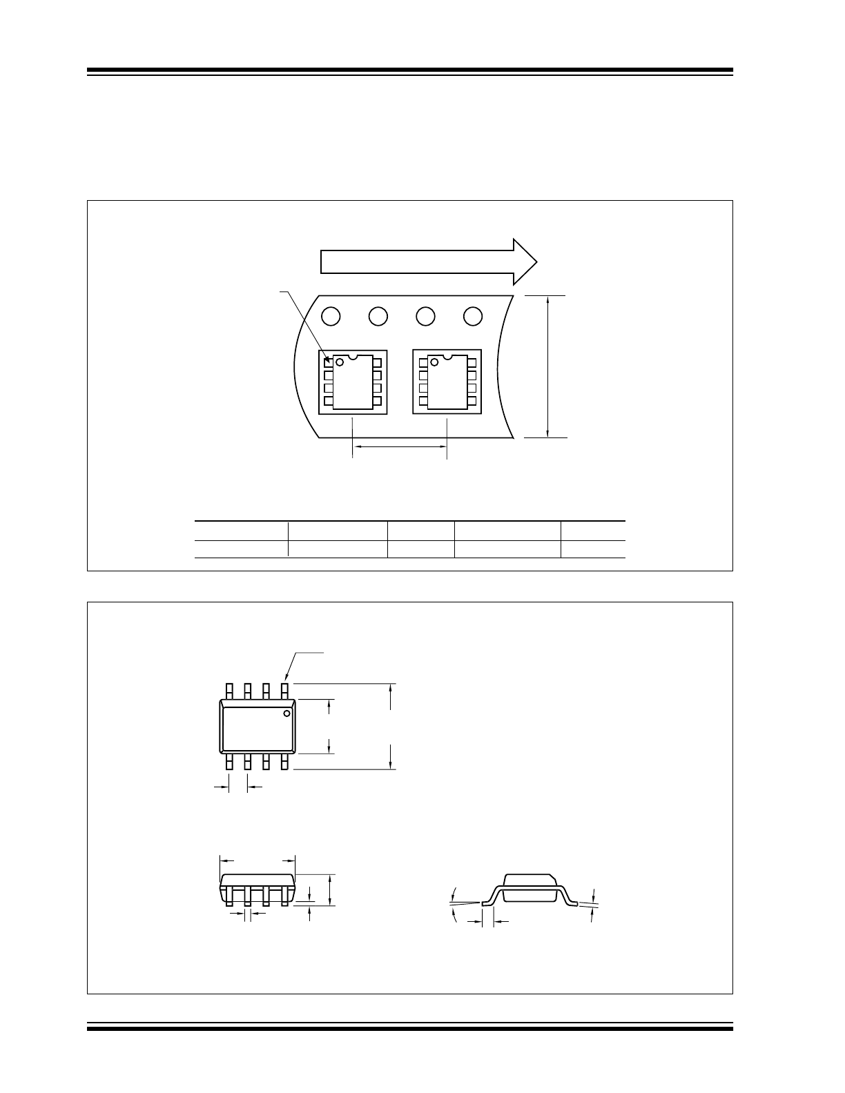
PACKAGING INFORMATION
6.1
Package Marking Information
Package marking data not available at this time.
6.2
Taping Form
6.3
Package Dimensions
Component Taping Orientation for 8-Pin SOIC (Narrow) Devices
Package
Carrier Width (W)
Pitch (P)
Part Per Full Reel
Reel Size
8-Pin SOIC (N)
12 mm
8 mm
2500
13 in
Carrier Tape, Number of Components Per Reel and Reel Size
Standard Reel Component Orientation
for TR Suffix Device
PIN 1
User Direction of Feed
P
W
.050 (1.27) TYP.
8
°
MAX.
PIN 1
.244 (6.20)
.228 (5.79)
.157 (3.99)
.150 (3.81)
.197 (5.00)
.189 (4.80)
.020 (0.51)
.013 (0.33)
.010 (0.25)
.004 (0.10)
.069 (1.75)
.053 (1.35)
.010 (0.25)
.007 (0.18)
.050 (1.27)
.016 (0.40)
.
8-Pin SOIC
Dimensions: inches (mm)
2002 Microchip Technology Inc.
DS21379B-page 9
TC1268
SALES AND SUPPORT
Data Sheets
Products supported by a preliminary Data Sheet may have an errata sheet describing minor operational differences and recom-
mended workarounds. To determine if an errata sheet exists for a particular device, please contact one of the following:
1.
Your local Microchip sales office
2.
The Microchip Corporate Literature Center U.S. FAX: (480) 792-7277
3.
The Microchip Worldwide Site (www.microchip.com)
Please specify which device, revision of silicon and Data Sheet (include Literature #) you are using.
New Customer Notification System
Register on our web site (www.microchip.com/cn) to receive the most current information on our products.

TC1268
DS21379B-page 10
2002 Microchip Technology Inc.
NOTES: