
© 2009 Microchip Technology Inc.
DS21974B-page 1
TC1313
Features
• Dual-Output Regulator (500 mA Buck Regulator
and 300 mA Low-Dropout Regulator (LDO))
• Total Device Quiescent Current = 57 µA (Typical)
• Independent Shutdown for Buck and LDO
Outputs
• Both Outputs Internally Compensated
• Synchronous Buck Regulator:
- Over 90% Typical Efficiency
- 2.0 MHz Fixed-Frequency PWM
(Heavy Load)
- Low Output Noise
- Automatic PWM-to-PFM mode transition
- Adjustable (0.8V to 4.5V) and Standard
Fixed-Output Voltages (0.8V, 1.2V, 1.5V,
1.8V, 2.5V, 3.3V)
• Low-Dropout Regulator:
- Low-Dropout Voltage = 137 mV Typical @
200 mA
- Standard Fixed-Output Voltages
(1.5V, 1.8V, 2.5V, 3.3V)
• Small 10-pin 3x3 DFN or MSOP Package Options
• Operating Junction Temperature Range:
- -40°C to +125°C
• Undervoltage Lockout (UVLO)
• Output Short Circuit Protection
• Overtemperature Protection
Applications
• Cellular Phones
• Portable Computers
• USB-Powered Devices
• Handheld Medical Instruments
• Organizers and PDAs
Description
The TC1313 device combines a 500 mA synchronous
buck regulator and 300 mA Low-Dropout Regulator
(LDO) to provide a highly integrated solution for
devices that require multiple supply voltages. The
unique combination of an integrated buck switching
regulator and low-dropout linear regulator provides the
lowest system cost for dual-output voltage applications
that require one lower processor core voltage and one
higher bias voltage.
The 500 mA synchronous buck regulator switches at a
fixed frequency of 2.0 MHz when the load is heavy,
providing a low-noise, small-size solution. When the
load on the buck output is reduced to light levels, it
changes operation to a Pulse Frequency Modulation
(PFM) mode to minimize quiescent current draw from
the battery. No intervention is necessary for smooth
transition from one mode to another.
The LDO provides a 300 mA auxiliary output that
requires a single 1 µF ceramic output capacitor,
minimizing board area and cost. The typical dropout
voltage for the LDO output is 137 mV for a 200 mA
load.
The TC1313 device is available in either the 10-pin DFN
or MSOP package.
Additional protection features include: UVLO,
overtemperature and overcurrent protection on both
outputs.
For a complete listing of TC1313 standard parts,
consult your Microchip representative.
Package Type
10-Lead DFN *
10-Lead MSOP
1
2
6
8
7
9
10
5
4
3
SHDN2
V
IN2
V
OUT2
A
GND
P
GND
L
X
V
IN1
SHDN1
V
FB1
/V
OUT1
NC
V
OUT2
V
IN2
NC
L
X
V
IN1
1
2
3
4
10
9
8
7
SHDN1
P
GND
SHDN2
EP
11
5
6
V
FB1
/V
OUT1
A
GND
* Includes Exposed Thermal Pad (EP); see
Table 3-1
.
500 mA Synchronous Buck Regulator,
+ 300 mA LDO
TC1313
DS21974B-page 2
© 2009 Microchip Technology Inc.
Functional Block Diagram
Synchronous Buck Regulator
NDRV
PDRV
P
GND
V
IN1
L
X
Driver
P
GND
Control
V
OUT1
/V
FB1
V
IN2
SHDN1
V
REF
LDO
V
OUT2
A
GND
A
GND
P
GND
Undervoltage Lockout
UVLO
UVLO
SHDN2
V
REF
(UVLO)
© 2009 Microchip Technology Inc.
DS21974B-page 3
TC1313
Typical Application Circuits
10-Lead DFN
4.7 µF
Input
Voltage
4.7 µH
4.7 µF
2.1V @
1 µF
3.3V @
4.5V to 5.5V
Adjustable-Output Application
121 kΩ
200 kΩ
4.99 kΩ
33 pF
1
2
6
8
7
9
10
5
4
3
SHDN2
V
IN2
V
OUT2
A
GND
P
GND
L
X
V
IN1
SHDN1
V
OUT1
NC
4.7 µF
4.7 µH
4.7 µF
1.5V @ 500 mA
1 µF
2.5V @ 300 mA
2.7V to 4.2V
TC1313
V
OUT1
V
OUT2
V
IN
V
OUT1
V
OUT2
1.0 µF
*Optional
Capacitor
V
IN2
300 mA
500 mA
Note:
Connect DFN package exposed pad to A
GND
.
10-Lead MSOP
Fixed-Output Application
TC1313
Note
V
OUT2
V
IN2
NC
L
X
8
2
7
1
9
10
6
3
SHDN1
P
GND
SHDN2
EP
11
4
5
V
OUT1
A
GND
V
IN1

TC1313
DS21974B-page 4
© 2009 Microchip Technology Inc.
NOTES:
© 2009 Microchip Technology Inc.
DS21974B-page 5
TC1313
1.0
ELECTRICAL
CHARACTERISTICS
Absolute Maximum Ratings †
V
IN
- A
GND
......................................................................6.0V
All Other I/O ...............................(A
GND
- 0.3V) to (V
IN
+ 0.3V)
L
X
to P
GND
...............................................-0.3V to (V
IN
+ 0.3V)
P
GND
to A
GND
.................................................. -0.3V to +0.3V
Output Short Circuit Current ................................ Continuous
Power Dissipation (Note 7) .......................... Internally Limited
Storage temperature .....................................-65°C to +150°C
Ambient Temp. with Power Applied ................-40°C to +85°C
Operating Junction Temperature...................-40°C to +125°C
ESD protection on all pins (HBM)
....................................... 3 kV
† Notice:
Stresses above those listed under “Maximum
Ratings” may cause permanent damage to the device. This is
a stress rating only and functional operation of the device at
those or any other conditions above those indicated in the
operational listings of this specification is not implied.
Exposure to maximum rating conditions for extended periods
may affect device reliability.
DC CHARACTERISTICS
Electrical Characteristics:
V
IN1
= V
IN2
= SHDN1,2 = 3.6V, C
OUT1
= C
IN
= 4.7 µF, C
OUT2
= 1µF, L
= 4.7 µH, V
OUT1
(ADJ) = 1.8V,
I
OUT1
= 100 ma, I
OUT2
= 0.1 mA T
A
= +25°C. Boldface specifications apply over the T
A
range of -40°C to +85°C.
Parameters
Sym
Min
Typ
Max
Units
Conditions
Input/Output Characteristics
Input Voltage
V
IN
2.7
—
5.5
V
Note 1
, Note 2, Note 8
Maximum Output Current
I
OUT1_MAX
500
—
—
mA
Note 1
Maximum Output Current
I
OUT2_MAX
300
—
—
mA
Note 1
Shutdown Current
Combined V
IN1
and V
IN2
Current
I
IN_SHDN
—
0.05
1
µA
SHDN1 = SHDN2 = GND
Operating I
Q
I
Q
—
57
100
µA
SHDN1 = SHDN2 = V
IN2
I
OUT1
= 0 mA, I
OUT2
= 0 mA
Synchronous Buck I
Q
—
38
—
µA
SHDN1 = V
IN
, SHDN2 = GND
LDO I
Q
—
44
—
µA
SHDN1 = GND, SHDN2 = V
IN2
Shutdown/UVLO/Thermal Shutdown Characteristics
SHDN1,SHDN2,
Logic Input Voltage Low
V
IL
—
—
15
%V
IN
V
IN1
= V
IN2
= 2.7V to 5.5V
SHDN1,SHDN2,
Logic Input Voltage High
V
IH
45
—
—
%V
IN
V
IN1
= V
IN2
= 2.7V to 5.5V
SHDN1,SHDN2,
Input Leakage Current
I
IN
-1.0
±0.01
1.0
µA
V
IN1
= V
IN2
= 2.7V to 5.5V
SHDNX = GND
SHDNY = V
IN
Thermal Shutdown
T
SHD
—
165
—
°C
Note 6
, Note 7
Thermal Shutdown Hysteresis
T
SHD-HYS
—
10
—
°C
Undervoltage Lockout
(V
OUT1
and V
OUT2
)
UVLO
2.4
2.55
2.7
V
V
IN1
Falling
Undervoltage Lockout Hysteresis
UVLO
-
HYS
—
200
—
mV
Note
1:
The Minimum V
IN
has to meet two conditions: V
IN
≥ 2.7V and V
IN
≥ V
RX
+ V
DROPOUT,
V
RX
= V
R1
or V
R2
.
2:
V
RX
is the regulator output voltage setting.
3:
TCV
OUT2
= ((V
OUT2max
– V
OUT2min
) * 10
6
)/(V
OUT2
* D
T
).
4:
Regulation is measured at a constant junction temperature using low duty cycle pulse testing. Load regulation is tested
over a load range from 0.1 mA to the maximum specified output current.
5:
Dropout voltage is defined as the input-to-output voltage differential at which the output voltage drops 2% below its
nominal value measured at a 1V differential.
6:
The maximum allowable power dissipation is a function of ambient temperature, the maximum allowable junction
temperature and the thermal resistance from junction to air. (i.e. T
A
, T
J
,
θ
JA
). Exceeding the maximum allowable power
dissipation causes the device to initiate thermal shutdown.
7:
The integrated MOSFET switches have an integral diode from the L
X
pin to V
IN
, and from L
X
to P
GND
. In cases where
these diodes are forward-biased, the package power dissipation limits must be adhered to. Thermal protection is not
able to limit the junction temperature for these cases.
8:
V
IN1
and V
IN2
are supplied by the same input source.
TC1313
DS21974B-page 6
© 2009 Microchip Technology Inc.
Synchronous Buck Regulator (V
OUT1
)
Adjustable Output Voltage Range
V
OUT1
0.8
—
4.5
V
Adjustable Reference Feedback
Voltage (V
FB1
)
V
FB1
0.78
0.8
0.82
V
Feedback Input Bias Current
(I
FB1
)
I
VFB1
—
-1.5
—
nA
Output Voltage Tolerance Fixed
(V
OUT1
)
V
OUT1
-2.5
±0.3
+2.5
%
Note 2
Line Regulation (V
OUT1
)
V
LINE-REG
—
0.2
—
%/V
V
IN
= V
R
+1V to 5.5V,
I
LOAD
= 100 mA
Load Regulation (V
OUT1
)
V
LOAD-REG
—
0.2
—
%
V
IN
= V
R
+ 1.5V, I
LOAD
= 100 mA to
500 mA (Note 1)
Dropout Voltage V
OUT1
V
IN
– V
OUT1
—
280
—
mV
I
OUT1
= 500 mA, V
OUT1
= 3.3V
(Note 5)
Internal Oscillator Frequency
F
OSC
1.6
2.0
2.4
MHz
Start Up Time
T
SS
—
0.5
—
ms
T
R
= 10% to 90%
R
DSon
P-Channel
R
DSon-P
—
450
—
m
Ω
I
P
= 100 mA
R
DSon
N-Channel
R
DSon-N
—
450
—
m
Ω
I
N
= 100 mA
L
X
Pin Leakage Current
I
LX
-1.0
±0.01
1.0
μA
SHDN = 0V, V
IN
= 5.5V, L
X
= 0V,
L
X
= 5.5V
Positive Current Limit Threshold
+I
LX(MAX)
—
700
—
mA
LDO Output (V
OUT2
)
Output Voltage Tolerance (V
OUT2
)
V
OUT2
-2.5
±0.3
+2.5
%
Note 2
Temperature Coefficient
TCV
OUT
—
25
—
ppm/°C
Note 3
Line Regulation
ΔV
OUT2
/
ΔV
IN
-0.2
±0.02
+0.2
%/V
(V
R
+1V)
≤ V
IN
≤ 5.5V
Load Regulation, V
OUT2
≥ 2.5V
ΔV
OUT2
/
I
OUT2
-0.75
0.1
+0.75
%
I
OUT2
= 0.1 mA to 300 mA
(Note 4)
Load Regulation, V
OUT2
< 2.5V
ΔV
OUT2
/
I
OUT2
-0.90
0.1
+0.90
%
I
OUT2
= 0.1 mA to 300 mA
(Note 4)
Dropout Voltage V
OUT2
> 2.5V
V
IN
– V
OUT2
—
137
300
mV
I
OUT2
= 200 mA (Note 5)
I
OUT2
= 300 mA
—
205
500
Power Supply Rejection Ratio
PSRR
—
62
—
dB
f
= 100 Hz, I
OUT1
= I
OUT2
= 50 mA,
C
IN
= 0 µF
Output Noise
eN
—
1.8
—
µV/(Hz)
½
f
= 1 kHz, I
OUT2
= 50 mA,
SHDN1 = GND
DC CHARACTERISTICS (CONTINUED)
Electrical Characteristics:
V
IN1
= V
IN2
= SHDN1,2 = 3.6V, C
OUT1
= C
IN
= 4.7 µF, C
OUT2
= 1µF, L
= 4.7 µH, V
OUT1
(ADJ) = 1.8V,
I
OUT1
= 100 ma, I
OUT2
= 0.1 mA T
A
= +25°C. Boldface specifications apply over the T
A
range of -40°C to +85°C.
Parameters
Sym
Min
Typ
Max
Units
Conditions
Note
1:
The Minimum V
IN
has to meet two conditions: V
IN
≥ 2.7V and V
IN
≥ V
RX
+ V
DROPOUT,
V
RX
= V
R1
or V
R2
.
2:
V
RX
is the regulator output voltage setting.
3:
TCV
OUT2
= ((V
OUT2max
– V
OUT2min
) * 10
6
)/(V
OUT2
* D
T
).
4:
Regulation is measured at a constant junction temperature using low duty cycle pulse testing. Load regulation is tested
over a load range from 0.1 mA to the maximum specified output current.
5:
Dropout voltage is defined as the input-to-output voltage differential at which the output voltage drops 2% below its
nominal value measured at a 1V differential.
6:
The maximum allowable power dissipation is a function of ambient temperature, the maximum allowable junction
temperature and the thermal resistance from junction to air. (i.e. T
A
, T
J
,
θ
JA
). Exceeding the maximum allowable power
dissipation causes the device to initiate thermal shutdown.
7:
The integrated MOSFET switches have an integral diode from the L
X
pin to V
IN
, and from L
X
to P
GND
. In cases where
these diodes are forward-biased, the package power dissipation limits must be adhered to. Thermal protection is not
able to limit the junction temperature for these cases.
8:
V
IN1
and V
IN2
are supplied by the same input source.
© 2009 Microchip Technology Inc.
DS21974B-page 7
TC1313
TEMPERATURE SPECIFICATIONS
Output Short Circuit Current
(Average)
I
OUTsc2
—
240
—
mA
R
LOAD2
≤ 1Ω
Wake-Up Time
(From SHDN2 mode), (V
OUT2
)
t
WK
—
31
100
µs
I
OUT1
= I
OUT2
= 50 mA
Settling Time
(From SHDN2 mode), (V
OUT2
)
t
S
—
100
—
µs
I
OUT1
= I
OUT2
= 50 mA
Electrical Specifications:
Unless otherwise indicated, all limits are specified for: V
IN
= +2.7V to +5.5V
Parameters
Sym
Min
Typ
Max
Units
Conditions
Temperature Ranges
Operating Junction Temperature Range
T
J
-40
—
+125
°C
Steady state
Storage Temperature Range
T
A
-65
—
+150
°C
Maximum Junction Temperature
T
J
—
—
+150
°C
Transient
Thermal Package Resistances
Thermal Resistance, 10L-DFN
θ
JA
—
41
—
°C/W
Typical 4-layer board with Internal
Ground Plane and 2 Vias in Thermal
Pad
Thermal Resistance, 10L-MSOP
θ
JA
—
113
—
°C/W
Typical 4-layer board with Internal
Ground Plane
DC CHARACTERISTICS (CONTINUED)
Electrical Characteristics:
V
IN1
= V
IN2
= SHDN1,2 = 3.6V, C
OUT1
= C
IN
= 4.7 µF, C
OUT2
= 1µF, L
= 4.7 µH, V
OUT1
(ADJ) = 1.8V,
I
OUT1
= 100 ma, I
OUT2
= 0.1 mA T
A
= +25°C. Boldface specifications apply over the T
A
range of -40°C to +85°C.
Parameters
Sym
Min
Typ
Max
Units
Conditions
Note
1:
The Minimum V
IN
has to meet two conditions: V
IN
≥ 2.7V and V
IN
≥ V
RX
+ V
DROPOUT,
V
RX
= V
R1
or V
R2
.
2:
V
RX
is the regulator output voltage setting.
3:
TCV
OUT2
= ((V
OUT2max
– V
OUT2min
) * 10
6
)/(V
OUT2
* D
T
).
4:
Regulation is measured at a constant junction temperature using low duty cycle pulse testing. Load regulation is tested
over a load range from 0.1 mA to the maximum specified output current.
5:
Dropout voltage is defined as the input-to-output voltage differential at which the output voltage drops 2% below its
nominal value measured at a 1V differential.
6:
The maximum allowable power dissipation is a function of ambient temperature, the maximum allowable junction
temperature and the thermal resistance from junction to air. (i.e. T
A
, T
J
,
θ
JA
). Exceeding the maximum allowable power
dissipation causes the device to initiate thermal shutdown.
7:
The integrated MOSFET switches have an integral diode from the L
X
pin to V
IN
, and from L
X
to P
GND
. In cases where
these diodes are forward-biased, the package power dissipation limits must be adhered to. Thermal protection is not
able to limit the junction temperature for these cases.
8:
V
IN1
and V
IN2
are supplied by the same input source.
TC1313
DS21974B-page 8
© 2009 Microchip Technology Inc.
2.0
TYPICAL PERFORMANCE CURVES
Note:
Unless otherwise indicated, V
IN1
= V
IN2
= SHDN1,2 = 3.6V, C
OUT1
= C
IN
= 4.7 µF, C
OUT2
= 1 µF, L
= 4.7 µH,
V
OUT1
(ADJ) = 1.8V, T
A
= +25°C. Boldface specifications apply over the T
A
range of -40°C to +85°C. T
A
= +25°C. Adjustable or fixed-
output voltage options can be used to generate the Typical Performance Characteristics.
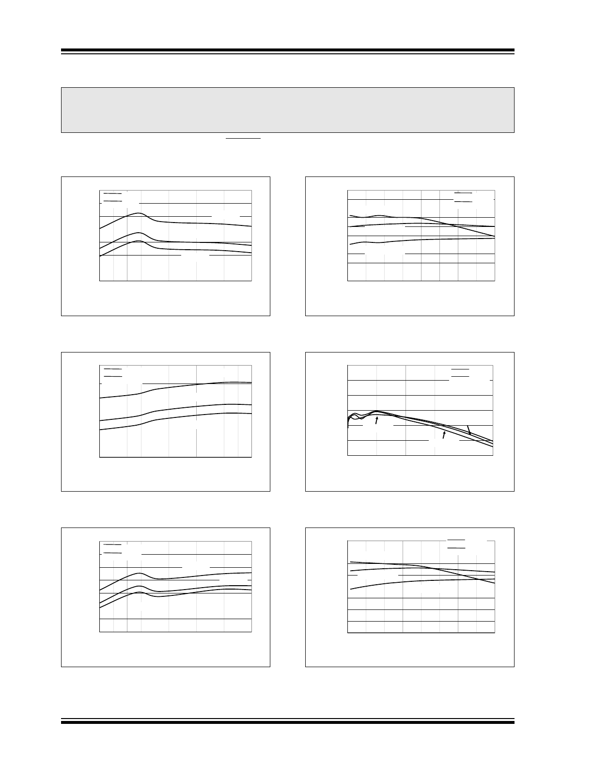
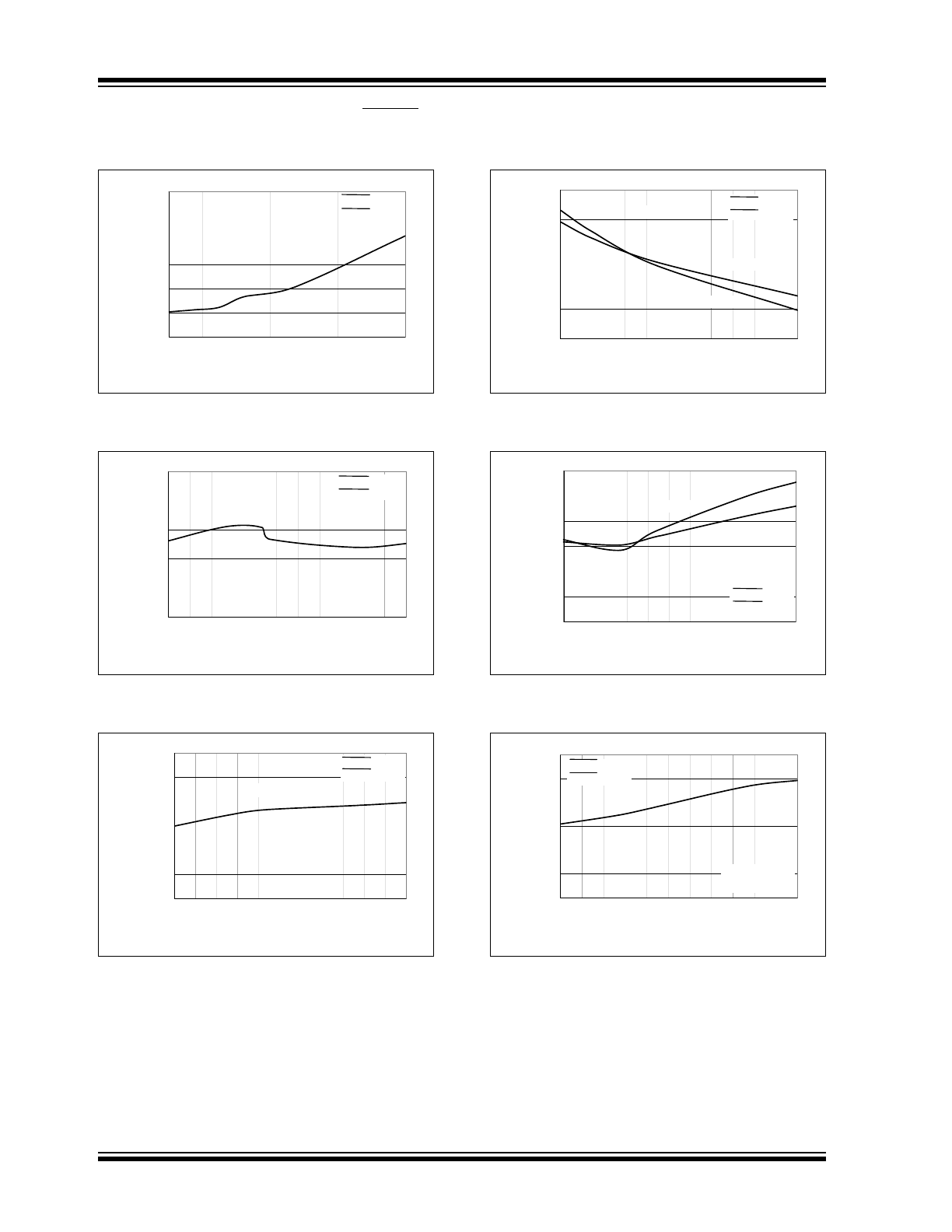
FIGURE 2-1:
I
Q
Switcher and LDO
Current vs. Ambient Temperature.
FIGURE 2-2:
I
Q
Switcher Current vs.
Ambient Temperature.
FIGURE 2-3:
I
Q
LDO Current vs. Ambient
Temperature.
FIGURE 2-4:
V
OUT1
Output Efficiency vs.
Input Voltage (V
OUT1
= 1.2V).
FIGURE 2-5:
V
OUT1
Output Efficiency vs.
I
OUT1
(V
OUT1
= 1.2V).
FIGURE 2-6:
V
OUT1
Output Efficiency vs.
Input Voltage (V
OUT1
= 1.8V).
Note:
The graphs and tables provided following this note are a statistical summary based on a limited number of
samples and are provided for informational purposes only. The performance characteristics listed herein
are not tested or guaranteed. In some graphs or tables, the data presented may be outside the specified
operating range (e.g., outside specified power supply range) and therefore outside the warranted range.
52
54
56
58
60
62
64
66
-40 -25 -10
5
20
35
50
65
80
95 110 125
Ambient Temperature (°C)
I
Q
Switch
er an
d
L
D
O (µ
A)
V
IN
= 5.5V
V
IN
= 4.2V
V
IN
= 3.6V
SHDN1 = V
IN2
SHDN2 = V
IN2
30
32
34
36
38
40
-40 -25 -10
5
20
35
50
65
80
95 110 125
Ambient Temperature (°C)
I
Q
Sw
it
ch
er
(
µ
A)
V
IN
= 5.5V
V
IN
= 4.2V
V
IN
= 3.6V
SHDN1 = V
IN2
SHDN2 = A
GND
36
38
40
42
44
46
48
50
-40 -25 -10
5
20
35
50
65
80
95 110 125
Ambient Temperature (°C)
I
Q
LD
O
(µ
A
)
V
IN
= 5.5V
V
IN
= 4.2V
V
IN
= 3.6V
SHDN1 = A
GND
SHDN2 = V
IN2
50
55
60
65
70
75
80
85
90
95
100
2.7
3.05
3.4
3.75
4.1
4.45
4.8
5.15
5.5
Input Voltage (V)
V
OU
T1
E
ffici
ency (%)
I
OUT1
= 100 mA
I
OUT1
= 250 mA
I
OUT1
= 500 mA
SHDN1 = V
IN2
SHDN2 = A
GND
70
75
80
85
90
95
100
0.005
0.104
0.203
0.302
0.401
0.5
I
OUT1
(A)
V
OU
T
1
E
ffi
ci
e
n
cy
(%)
V
IN1
= 3.0V
V
IN1
= 4.2V
V
IN1
= 3.6V
SHDN1 = V
IN2
SHDN2 = A
GND
60
65
70
75
80
85
90
95
100
2.7
3.05
3.4
3.75
4.1
4.45
4.8
5.15
5.5
Input Voltage (V)
V
OU
T
1
E
ffi
ci
en
cy
(%
)
I
OUT1
= 100 mA
I
OUT1
= 250 mA
I
OUT1
= 500 mA
SHDN1 = V
IN2
SHDN2 = A
GND
© 2009 Microchip Technology Inc.
DS21974B-page 9
TC1313
Note:
Unless otherwise indicated, V
IN1
= V
IN2
= SHDN1,2 = 3.6V, C
OUT1
= C
IN
= 4.7 µF, C
OUT2
= 1 µF, L
= 4.7 µH,
V
OUT1
(ADJ) = 1.8V, T
A
= +25°C. Boldface specifications apply over the T
A
range of -40°C to +85°C. T
A
= +25°C. Adjustable or fixed-
output voltage options can be used to generate the Typical Performance Characteristics.
FIGURE 2-7:
V
OUT1
Output Efficiency vs.
I
OUT1
(V
OUT1
= 1.8V).
FIGURE 2-8:
V
OUT1
Output Efficiency vs.
Input Voltage (V
OUT1
= 3.3V).
FIGURE 2-9:
V
OUT1
Output Efficiency vs.
I
OUT1
(V
OUT1
= 3.3V).
FIGURE 2-10:
V
OUT1
vs. I
OUT1
(V
OUT1
= 1.2V).
FIGURE 2-11:
V
OUT1
vs. I
OUT1
(V
OUT1
= 1.8V).
FIGURE 2-12:
V
OUT1
vs. I
OUT1
(V
OUT1
= 3.3V).
75
80
85
90
95
100
0.005
0.104
0.203
0.302
0.401
0.5
I
OUT1
(A)
V
OU
T1
Efficienc
y
(%
)
SHDN1 = V
IN2
SHDN2 = A
GND
V
IN
= 3.0V
V
IN
= 4.2V
V
IN
= 3.6V
80
84
88
92
96
100
3.60
3.92
4.23
4.55
4.87
5.18
5.50
Input Voltage (V)
V
OUT1
E
ffi
ci
e
n
cy
(%
)
I
OUT1
= 100 mA
I
OUT1
= 250 mA
I
OUT1
= 500 mA
SHDN1 = V
IN2
SHDN2 = A
GND
60
65
70
75
80
85
90
95
100
0.005
0.104
0.203
0.302
0.401
0.5
I
OUT1
(A)
V
OU
T
1
E
ffi
ci
e
n
c
y
(%)
V
IN1
= 5.5V
SHDN1 = V
IN2
SHDN2 = A
GND
V
IN1
= 4.2V
V
IN1
= 3.6V
1.19
1.194
1.198
1.202
1.206
1.21
0.005
0.104
0.203
0.302
0.401
0.5
I
OUT1
(A)
V
OU
T1
(V
)
SHDN1 = V
IN2
SHDN2 = A
GND
V
IN1
= 3.6V
1.79
1.795
1.8
1.805
1.81
1.815
1.82
0.005
0.104
0.203
0.302
0.401
0.5
I
OUT1
(A)
V
OU
T1
(V
)
SHDN1 = V
IN2
SHDN2 = A
GND
V
IN1
= 3.6V
3.2
3.24
3.28
3.32
3.36
3.4
0.005
0.104
0.203
0.302
0.401
0.5
I
OUT1
(A)
V
OUT
1
(V)
SHDN1 = V
IN2
SHDN2 = A
GND
V
IN1
= 4.2V
TC1313
DS21974B-page 10
© 2009 Microchip Technology Inc.
Note:
Unless otherwise indicated, V
IN1
= V
IN2
= SHDN1,2 = 3.6V, C
OUT1
= C
IN
= 4.7 µF, C
OUT2
= 1 µF, L
= 4.7 µH,
V
OUT1
(ADJ) = 1.8V, T
A
= +25°C. Boldface specifications apply over the T
A
range of -40°C to +85°C. T
A
= +25°C. Adjustable or fixed-
output voltage options can be used to generate the Typical Performance Characteristics.
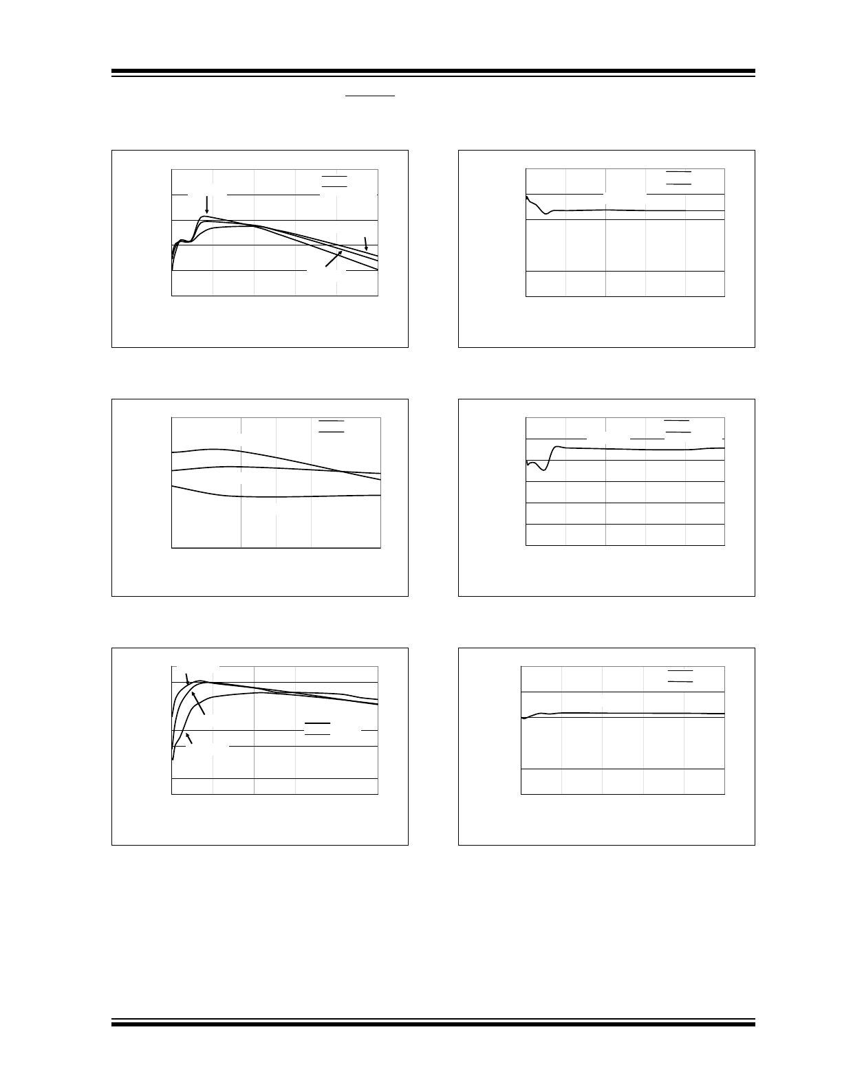
FIGURE 2-13:
V
OUT1
Switching Frequency
vs. Input Voltage.
FIGURE 2-14:
V
OUT1
Switching Frequency
vs. Ambient Temperature.
FIGURE 2-15:
V
OUT1
Adjustable Feedback
Voltage vs. Ambient Temperature.
FIGURE 2-16:
V
OUT1
Switch Resistance
vs. Input Voltage.
FIGURE 2-17:
V
OUT1
Switch Resistance
vs. Ambient Temperature.
FIGURE 2-18:
V
OUT1
Dropout Voltage vs.
Ambient Temperature.
1.90
1.95
2.00
2.05
2.10
2.15
2.20
2.7
3.1
3.5
3.9
4.3
4.7
5.1
5.5
Input Voltage (V)
V
OU
T1
F
re
q
ue
nc
y
(
M
H
z
)
SHDN1 = V
IN2
SHDN2 = A
GND
1.90
1.92
1.94
1.96
1.98
2.00
-40
-25
-10
5
20
35
50
65
80
95
11
0
12
5
Ambient Temperature (°C)
V
OUT1
Fr
e
que
ncy
(MH
z
)
SHDN1 = V
IN2
SHDN2 = A
GND
0.790
0.795
0.800
0.805
0.810
0.815
0.820
-40
-25
-10
5
20
35
50
65
80
95
11
0
12
5
Ambient Temperature (°C)
V
OUT1
FB
Voltage
(V)
SHDN1 = V
IN2
SHDN2 = A
GND
V
IN1
= 3.6V
0.40
0.45
0.50
0.55
0.60
0.65
3.3 3.5 3.7 3.9 4.1 4.3 4.5 4.7 4.9 5.1 5.3 5.5
Input Voltage (V)
V
OUT1
Switch Resistance (
:
)
SHDN1 = V
IN2
SHDN2 = A
GND
V
IN1
= 3.6V
N-Channel
P-Channel
0.40
0.45
0.50
0.55
0.60
0.65
0.70
-40 -25 -10 5
20 35 50 65 80 95 110 125
Ambient Temperature (°C)
Buck Regulator Switch
Resistance (
:
)
V
IN1
= 3.6V
N-Channel
P-Channel
SHDN1 = V
IN2
SHDN2 = A
GND
0.1
0.15
0.2
0.25
0.3
0.35
0.4
-40
-25
-10
5
20
35
50
65
80
95
11
0
12
5
Ambient Temperature (°C)
V
OU
T1
Dropout
Voltage (V)
SHDN1 = V
IN2
SHDN2 = A
GND
V
OUT1
= 3.3V
I
OUT1
= 500 mA