
© 2007 Microchip Technology Inc.
DS21354D-page 1
TC1072/TC1073
Features:
• 50 µA Ground Current for Longer Battery Life
• Very Low Dropout Voltage
• Choice of 50 mA (TC1072) and 100 mA (TC1073)
Output
• High Output Voltage Accuracy
• Standard or Custom Output Voltages
• Power-Saving Shutdown Mode
• ERROR Output Can Be Used as a Low Battery
Detector or Processor Reset Generator
• Bypass Input for Ultra Quiet Operation
• Overcurrent and Overtemperature Protection
• Space-Saving 6-Pin SOT-23 Package
• Pin Compatible Upgrades for Bipolar Regulators
• Standard Output Voltage Options:
- 1.8V, 2.5V, 2.6V, 2.7V, 2.8V, 2.85V, 3.0V,
3.3V, 3.6V, 4.0V, 5.0V
• Other output voltages are available. Please
contact Microchip Technology Inc. for details.
Applications:
• Battery Operated Systems
• Portable Computers
• Medical Instruments
• Instrumentation
• Cellular/GSM/PHS Phones
• Linear Post-Regulators for SMPS
• Pagers
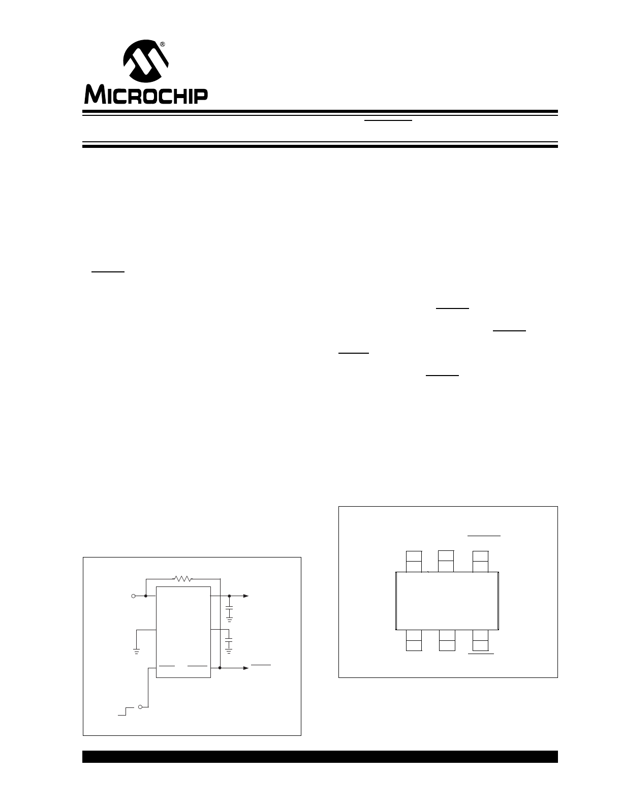
Typical Application Circuit
General Description
The TC1072 and TC1073 are high accuracy (typically
±0.5%) CMOS upgrades for older (bipolar) low dropout
regulators. Designed specifically for battery-operated
systems, the devices’ CMOS construction eliminates
wasted ground current, significantly extending battery
life. Total supply current is typically 50 µA at full load
(20 to 60 times lower than in bipolar regulators).
The devices’ key features include ultra low noise
operation (plus optional Bypass input); very low
dropout voltage (typically 85 mV, TC1072 and 180 mV,
TC1073 at full load) and fast response to step changes
in load. An error output (ERROR) is asserted when the
devices are out-of-regulation (due to a low input
voltage or excessive output current). ERROR can be
used as a low battery warning or as a processor
RESET signal (with the addition of an external RC
network). Supply current is reduced to 0.5 µA (max)
and both V
OUT
and ERROR are disabled when the
shutdown input is low. The devices incorporate both
overtemperature and overcurrent protection.
The TC1072 and TC1073 are stable with an output
capacitor of only 1 µF and have a maximum output
current of 50 mA, and 100 mA, respectively. For higher
output current versions, please see the TC1185,
TC1186, TC1187 (I
OUT
= 150 mA) and TC1107,
TC1108 and TC1173 (I
OUT
= 300 mA) data sheets.
Package Type
TC1072
TC1073
V
OUT
GND
1
µ
F
+
V
IN
V
IN
V
OUT
1
6
2
4
3
SHDN
Shutdown Control
(from Power Control Logic)
ERROR
ERROR
Bypass
C
BYPASS
470 pF
5
R
P
6
1
4
2
3
6-Pin SOT-23
V
OUT
ERROR
SHDN
GND
V
IN
5
Bypass
50mA and 100mA CMOS LDOs with Shutdown, ERROR Output and V
REF
Bypass
TC1072/TC1073
DS21354D-page 2
© 2007 Microchip Technology Inc.
1.0
ELECTRICAL
CHARACTERISTICS
Absolute Maximum Ratings†
Input Voltage .........................................................6.5V
Output Voltage........................... (-0.3V) to (V
IN
+ 0.3V)
Power Dissipation................Internally Limited (Note 6)
Maximum Voltage on Any Pin ........V
IN
+0.3V to -0.3V
Operating Temperature Range...... -40°C < T
J
< 125°C
Storage Temperature..........................-65°C to +150°C
† Note: Stresses above those listed under "Absolute
Maximum Ratings" may cause permanent damage to
the device. These are stress ratings only and functional
operation of the device at these or any other conditions
above those indicated in the operation sections of the
specifications is not implied. Exposure to Absolute
Maximum Rating conditions for extended periods may
affect device reliability.
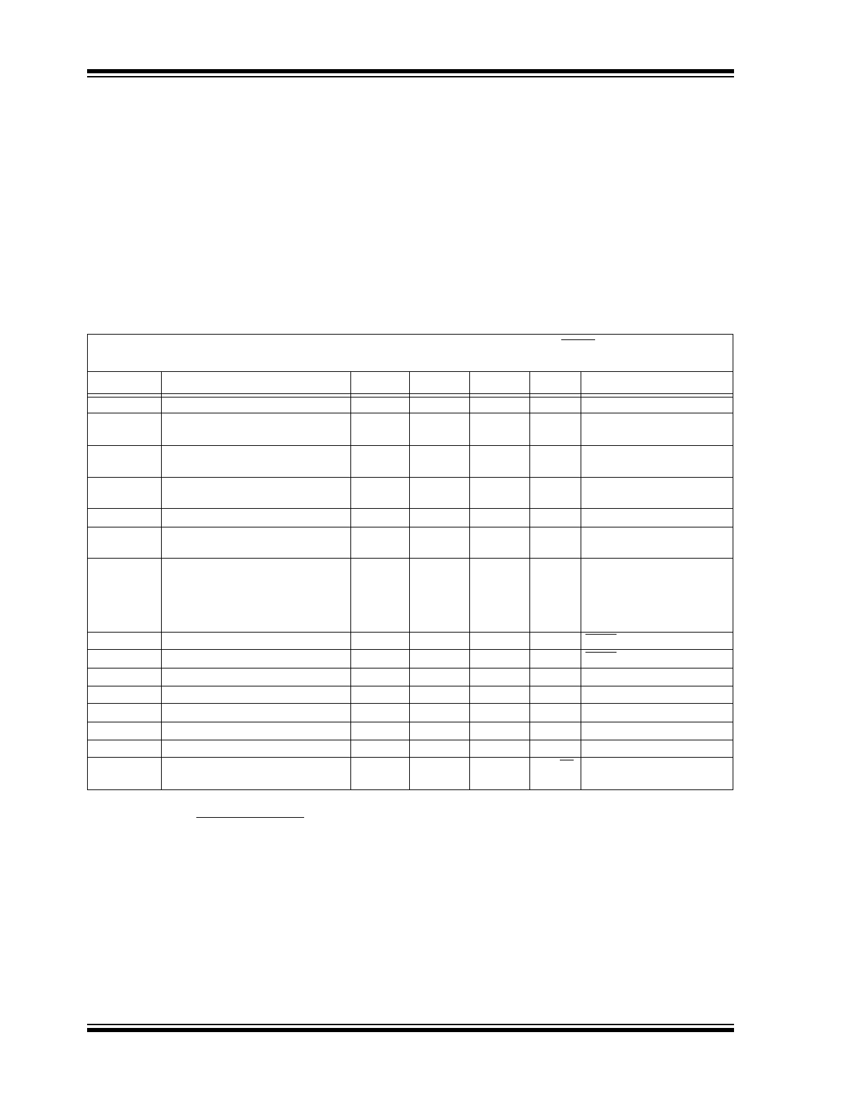
TC1072/TC1073 ELECTRICAL SPECIFICATIONS
Electrical Characteristics: Unless otherwise noted, V
IN
= V
OUT
+ 1V, I
L
= 0.1 mA, C
L
= 3.3
μF, SHDN > V
IH
, T
A
= +25°C.
Boldface type specifications apply for junction temperatures of -40°C to +125°C.
Symbol
Parameter
Min
Typ
Max
Units
Test Conditions
V
IN
Input Operating Voltage
2.7
—
6.0
V
Note 9
I
OUT
MAX
Maximum Output Current
50
100
—
—
—
—
mA
mA
TC1072
TC1073
V
OUT
Output Voltage
V
R
–
2.5%
V
R
±0.5% V
R
+ 2.5%
V
Note 1
TCV
OUT
V
OUT
Temperature Coefficient
—
—
20
40
—
—
ppm/°C Note 2
ΔV
OUT
/
ΔV
IN
Line Regulation
—
0.05
0.35
%
(V
R
+ 1V)
≤ V
IN
≤ 6V
ΔV
OUT
/V
OUT
Load Regulation
—
0.5
2.0
%
I
L
= 0.1 mA to I
OUT
MAX
(Note 3)
V
IN
-V
OUT
Dropout Voltage
—
—
—
—
2
65
85
180
—
—
120
250
mV
I
L
= 0.1 mA
I
L
= 20 mA
I
L
= 50 mA
I
L
= 100 mA (Note 4),
TC1073
I
IN
Supply Current
—
50
80
µA
SHDN = V
IH
, I
L
= 0 (Note 8)
I
INSD
Shutdown Supply Current
—
0.05
0.5
µA
SHDN = 0V
PSRR
Power Supply Rejection Ratio
—
64
—
dB
F
RE
≤ 1 kHz
I
OUT
SC
Output Short Circuit Current
—
300
450
mA
V
OUT
= 0V
ΔV
OUT
/
ΔP
D
Thermal Regulation
—
0.04
—
V/W
Notes 5, 6
T
SD
Thermal Shutdown Die Temperature
—
160
—
°C
ΔT
SD
Thermal Shutdown Hysteresis
—
10
—
°C
eN
Output Noise
—
260
—
nV/
√Hz I
L
= I
OUT
MAX
470 pF from Bypass to GND
Note
1:
V
R
is the regulator output voltage setting. For example: V
R
= 2.5V, 2.7V, 2.85V, 3.0V, 3.3V, 3.6V, 4.0V, 5.0V.
2:
3:
Regulation is measured at a constant junction temperature using low duty cycle pulse testing. Load regulation is tested over a load range
from 0.1 mA to the maximum specified output current. Changes in output voltage due to heating effects are covered by the thermal
regulation specification.
4:
Dropout voltage is defined as the input to output differential at which the output voltage drops 2% below its nominal value.
5:
Thermal Regulation is defined as the change in output voltage at a time T after a change in power dissipation is applied, excluding load or
line regulation effects. Specifications are for a current pulse equal to I
L
MAX
at V
IN
= 6V for T = 10 ms.
6:
The maximum allowable power dissipation is a function of ambient temperature, the maximum allowable junction temperature and the
thermal resistance from junction-to-air (i.e., T
A
, T
J
,
θ
JA
). Exceeding the maximum allowable power dissipation causes the device to initiate
thermal shutdown. Please see Section 5.0 “Thermal Considerations” for more details.
7:
Hysteresis voltage is referenced by V
R
.
8:
Apply for Junction Temperatures of -40°C to +85°C.
9:
The minimum V
IN
has to justify the conditions = V
IN
≥ V
R
+ V
DROPOUT
and V
IN
≥ 2.7V for I
L
= 0.1 mA to I
OUT
MAX
.
TC V
OUT
= (V
OUT
MAX
– V
OUT
MIN
) x 10
6
V
OUT
x
ΔT
© 2007 Microchip Technology Inc.
DS21354D-page 3
TC1072/TC1073
SHDN Input
V
IH
SHDN Input High Threshold
45
—
—
%V
IN
V
IN
= 2.5V to 6.5V
V
IL
SHDN Input Low Threshold
—
—
15
%V
IN
V
IN
= 2.5V to 6.5V
ERROR Open Drain Output
V
IN
MIN
Minimum V
IN
Operating Voltage
1.0
—
—
V
V
OL
Output Logic Low Voltage
—
—
400
mV
1 mA Flows to ERROR
V
TH
ERROR Threshold Voltage
—
0.95 x V
R
—
V
See
Figure 4-2
V
HYS
ERROR Positive Hysteresis
—
50
—
mV
Note 7
t
DELAY
V
OUT
to ERROR Delay
—
2.5
—
ms
Vout falling from V
R
to
V
R
-10%
TC1072/TC1073 ELECTRICAL SPECIFICATIONS (CONTINUED)
Electrical Characteristics: Unless otherwise noted, V
IN
= V
OUT
+ 1V, I
L
= 0.1 mA, C
L
= 3.3
μF, SHDN > V
IH
, T
A
= +25°C.
Boldface type specifications apply for junction temperatures of -40°C to +125°C.
Symbol
Parameter
Min
Typ
Max
Units
Test Conditions
Note
1:
V
R
is the regulator output voltage setting. For example: V
R
= 2.5V, 2.7V, 2.85V, 3.0V, 3.3V, 3.6V, 4.0V, 5.0V.
2:
3:
Regulation is measured at a constant junction temperature using low duty cycle pulse testing. Load regulation is tested over a load range
from 0.1 mA to the maximum specified output current. Changes in output voltage due to heating effects are covered by the thermal
regulation specification.
4:
Dropout voltage is defined as the input to output differential at which the output voltage drops 2% below its nominal value.
5:
Thermal Regulation is defined as the change in output voltage at a time T after a change in power dissipation is applied, excluding load or
line regulation effects. Specifications are for a current pulse equal to I
L
MAX
at V
IN
= 6V for T = 10 ms.
6:
The maximum allowable power dissipation is a function of ambient temperature, the maximum allowable junction temperature and the
thermal resistance from junction-to-air (i.e., T
A
, T
J
,
θ
JA
). Exceeding the maximum allowable power dissipation causes the device to initiate
thermal shutdown. Please see Section 5.0 “Thermal Considerations” for more details.
7:
Hysteresis voltage is referenced by V
R
.
8:
Apply for Junction Temperatures of -40°C to +85°C.
9:
The minimum V
IN
has to justify the conditions = V
IN
≥ V
R
+ V
DROPOUT
and V
IN
≥ 2.7V for I
L
= 0.1 mA to I
OUT
MAX
.
TC V
OUT
= (V
OUT
MAX
– V
OUT
MIN
) x 10
6
V
OUT
x
ΔT
TC1072/TC1073
DS21354D-page 4
© 2007 Microchip Technology Inc.
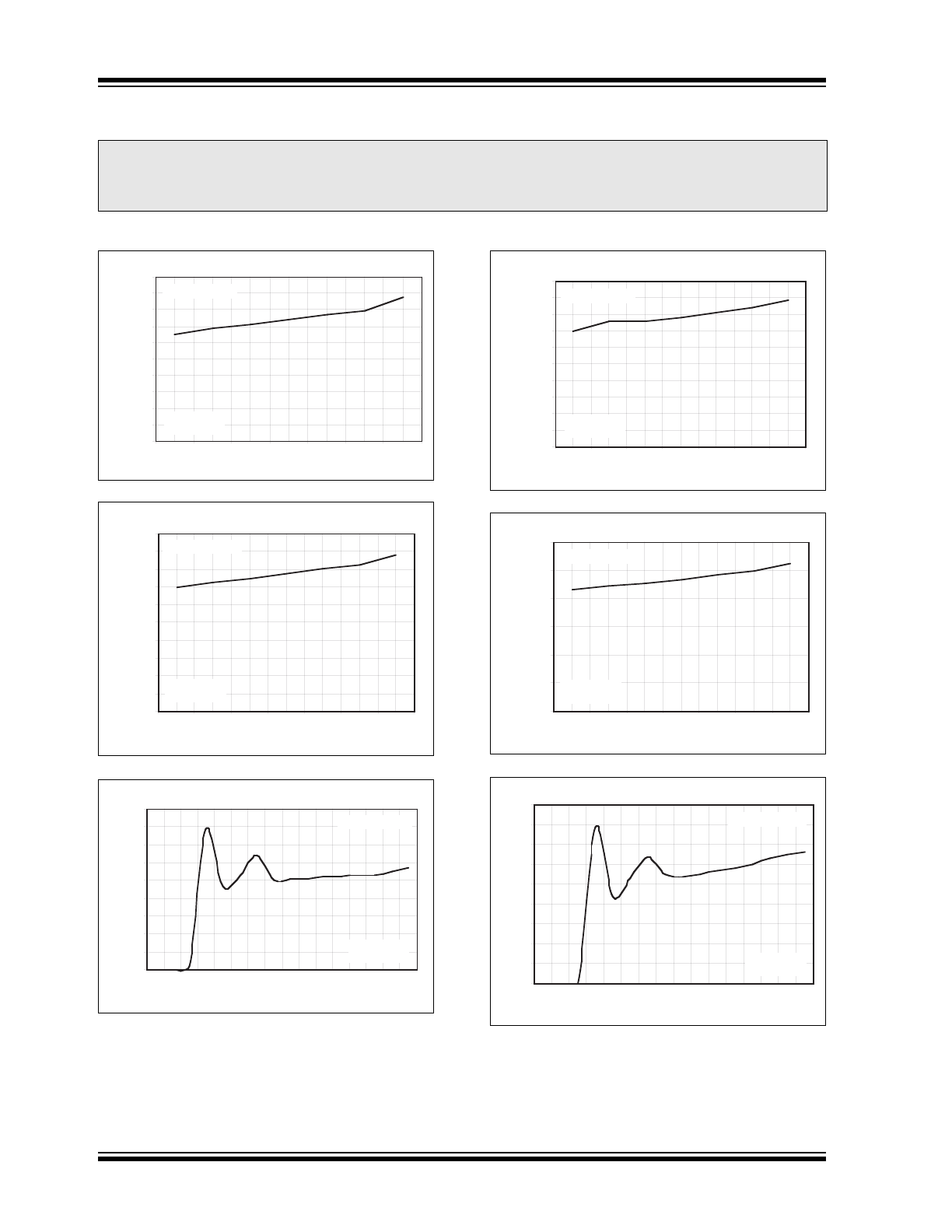
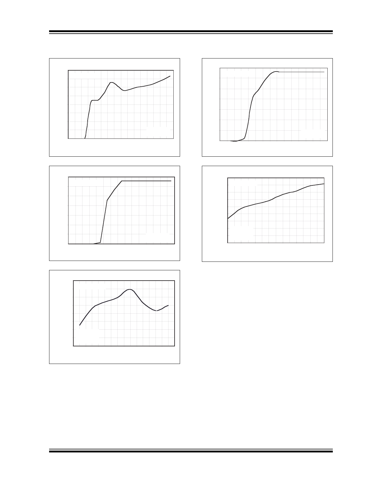
2.0
TYPICAL CHARACTERISTICS CURVES
Note: Unless otherwise specified, all parts are measured at temperature = +25°C.
Note:
The graphs and tables provided following this note are a statistical summary based on a limited number of
samples and are provided for informational purposes only. The performance characteristics listed herein
are not tested or guaranteed. In some graphs or tables, the data presented may be outside the specified
operating range (e.g., outside specified power supply range) and therefore outside the warranted range.
0.000
0.002
0.004
0.006
0.008
0.010
0.012
0.014
0.016
0.018
0.020
-40
-20
0
20
50
70
125
DROPOUT VOLTAGE (V)
I
LOAD
= 10mA
C
IN
= 1
μF
C
OUT
= 1
μF
TEMPERATURE (
°C)
Dropout Voltage vs. Temperature (V
OUT
= 3.3V)
0.000
0.020
0.040
0.060
0.080
0.100
0.120
0.140
0.160
0.180
0.200
-40
-20
0
20
50
70
125
DROPOUT VOLTAGE (V)
I
LOAD
= 100mA
C
IN
= 1
μF
C
OUT
= 1
μF
TEMPERATURE (
°C)
Dropout Voltage vs. Temperature (V
OUT
= 3.3V)
0
10
20
30
40
50
60
70
80
90
GND CURRENT (
μ
A)
0 0.5 1 1.5 2 2.5 3 3.5 4 4.5 5 5.5 6 6.5 7 7.5
I
LOAD
= 10mA
C
IN
= 1
μF
C
OUT
= 1
μF
Ground Current vs. V
IN
(V
OUT
= 3.3V)
V
IN
(V)
0.000
0.010
0.020
0.030
0.040
0.050
0.060
0.070
0.080
0.090
0.100
-40
-20
0
20
50
70
125
DROPOUT VOLTAGE (V)
I
LOAD
= 50mA
C
IN
= 1
μF
C
OUT
= 1
μF
TEMPERATURE (
°C)
Dropout Voltage vs. Temperature (V
OUT
= 3.3V)
0.000
0.050
0.100
0.150
0.200
0.250
0.300
-40
-20
0
20
50
70
125
DROPOUT VOLTAGE (V)
I
LOAD
= 150mA
C
IN
= 1
μF
C
OUT
= 1
μF
TEMPERATURE (
°C)
Dropout Voltage vs. Temperature (V
OUT
= 3.3V)
0
10
20
30
40
50
60
70
80
90
GND CURRENT (
μ
A)
0 0.5 1 1.5 2 2.5 3 3.5 4 4.5 5 5.5 6 6.5 7 7.5
I
LOAD
= 100mA
C
IN
= 1
μF
C
OUT
= 1
μF
Ground Current vs. V
IN
(V
OUT
= 3.3V)
V
IN
(V)
© 2007 Microchip Technology Inc.
DS21354D-page 5
TC1072/TC1073
Note: Unless otherwise specified, all parts are measured at temperature = +25°C.
0
10
20
30
40
50
60
70
80
GND CURRENT (
μ
A)
0 0.5 1 1.5 2 2.5 3 3.5 4 4.5 5 5.5 6 6.5 7 7.5
I
LOAD
= 150mA
C
IN
= 1
μF
C
OUT
= 1
μF
V
IN
(V)
Ground Current vs. V
IN
(V
OUT
= 3.3V)
0.0
0.5
1.0
1.5
2.0
2.5
3.0
3.5
I
LOAD
= 100mA
C
IN
= 1
μF
C
OUT
= 1
μF
0 0.5 1 1.5 2 2.5 3 3.5 4 4.5 5 5.5 6 6.5 7
V
IN
(V)
V
OUT
(V)
V
OUT
vs.
V
IN
(V
OUT
= 3.3V)
3.274
3.276
3.278
3.280
3.282
3.284
3.286
3.288
3.290
-40
-20
-10
0
20
40
85
125
I
LOAD
= 150mA
C
IN
= 1
μF
C
OUT
= 1
μF
V
IN
= 4.3V
TEMPERATURE (
°C)
V
OUT
(V)
Output Voltage vs. Temperature (V
OUT
= 3.3V)
0
0.5
1
1.5
2
2.5
3
3.5
0 0.5 1 1.5 2 2.5 3 3.5 4 4.5 5 5.5 6 6.5 7
I
LOAD
= 0
C
IN
= 1
μF
C
OUT
= 1
μF
V
IN
(V)
V
OUT
(V)
V
OUT
vs.
V
IN
(V
OUT
= 3.3V)
3.275
3.280
3.285
3.290
3.295
3.300
3.305
3.310
3.315
3.320
-40
-20
-10
0
20
40
85
125
I
LOAD
= 10mA
C
IN
= 1
μF
C
OUT
= 1
μF
V
IN
= 4.3V
TEMPERATURE (
°C)
V
OUT
(V)
Output Voltage vs. Temperature (V
OUT
= 3.3V)
TC1072/TC1073
DS21354D-page 6
© 2007 Microchip Technology Inc.
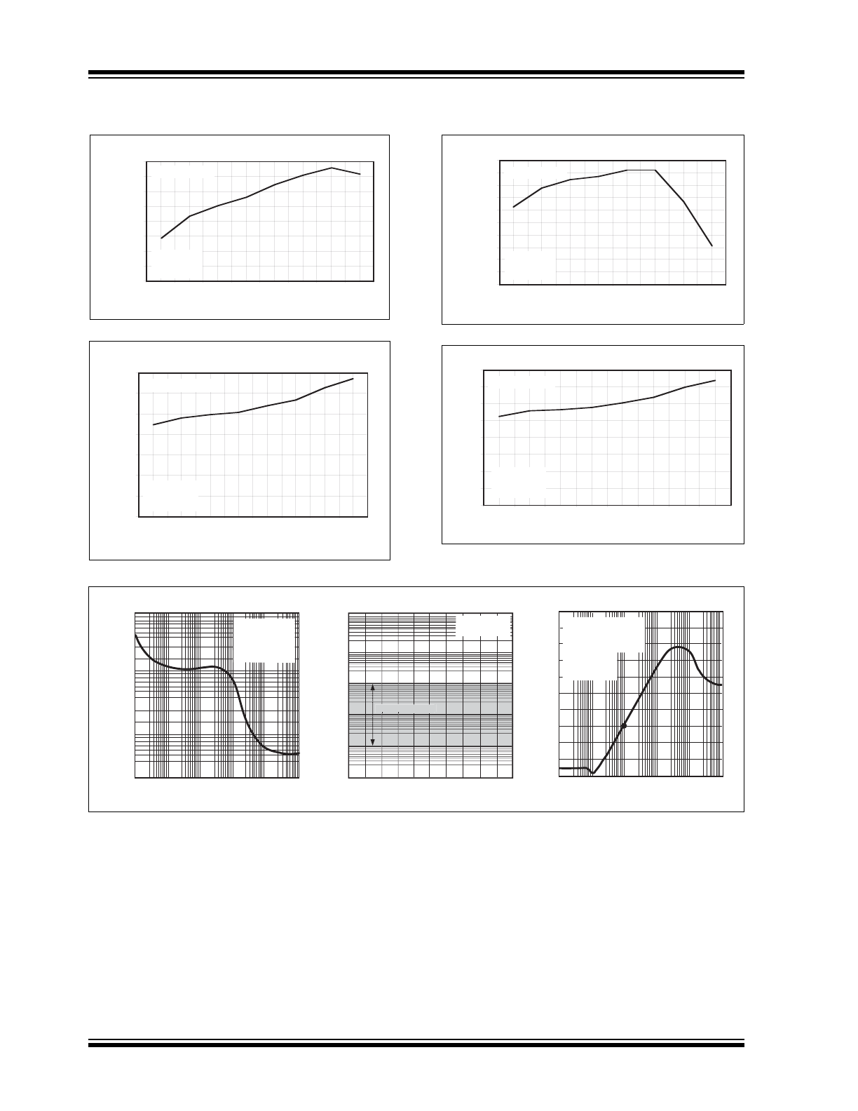
Note: Unless otherwise specified, all parts are measured at temperature = +25°C.
4.985
4.990
4.995
5.000
5.005
5.010
5.015
5.020
5.025
-40
-20
-10
0
20
40
85
125
I
LOAD
= 10mA
V
IN
= 6V
C
IN
= 1
μF
C
OUT
= 1
μF
TEMPERATURE (
°C)
Output Voltage vs. Temperature (V
OUT
= 5V)
V
OUT
(V)
0
10
20
30
40
50
60
70
-40
-20
-10
0
20
40
85
125
GND CURRENT (
μ
A)
I
LOAD
= 10mA
V
IN
= 6V
C
IN
= 1
μF
C
OUT
= 1
μF
TEMPERATURE (
°C)
Temperature
vs. Quiescent Current (V
OUT
= 5V)
4.974
4.976
4.978
4.980
4.982
4.984
4.986
4.988
4.990
4.992
4.994
-40
-20
-10
0
20
40
85
125
I
LOAD
= 150mA
V
IN
= 6V
C
IN
= 1
μF
C
OUT
= 1
μF
TEMPERATURE (
°C)
Output Voltage vs. Temperature (V
OUT
= 5V)
V
OUT
(V)
Temperature vs. Quiescent Current (V
OUT
= 5V)
0
10
20
30
40
50
60
70
80
-40
-20
-10
0
20
40
85
125
GND CURRENT (
μ
A)
I
LOAD
= 150mA
V
IN
= 6V
C
IN
= 1
μF
C
OUT
= 1
μF
TEMPERATURE (
°C)
10.0
1.0
0.1
0.0
0.01K 0.1K
1K
10K
100K
1000K
FREQUENCY (Hz)
Output Noise vs. Frequency
NOISE (
μ
V/
√
Hz)
R
LOAD
= 50
Ω
C
OUT
= 1
μF
C
IN
= 1
μF
C
BYP
= 0
1000
100
10
1
0.1
0.01
0
10 20 30 40 50 60 70 80 90 100
LOAD CURRENT (mA)
Stability Region vs. Load Current
C
OUT
ESR
(Ω
)
C
OUT
= 1
μF
to 10
μF
Stable Region
Stable Region
-30
-35
-40
-45
-50
-60
-55
-65
-70
-75
-80
0.01K 0.1K
1K
10K
100K 1000K
FREQUENCY (Hz)
Power Supply Rejection Ratio
PSRR (dB)
I
OUT
=
10mA
V
INDC
=
4V
V
INAC
=
100mVp-p
V
OUT
=
3V
C
IN
=
0
C
OUT
=
1
μF
© 2007 Microchip Technology Inc.
DS21354D-page 7
TC1072/TC1073
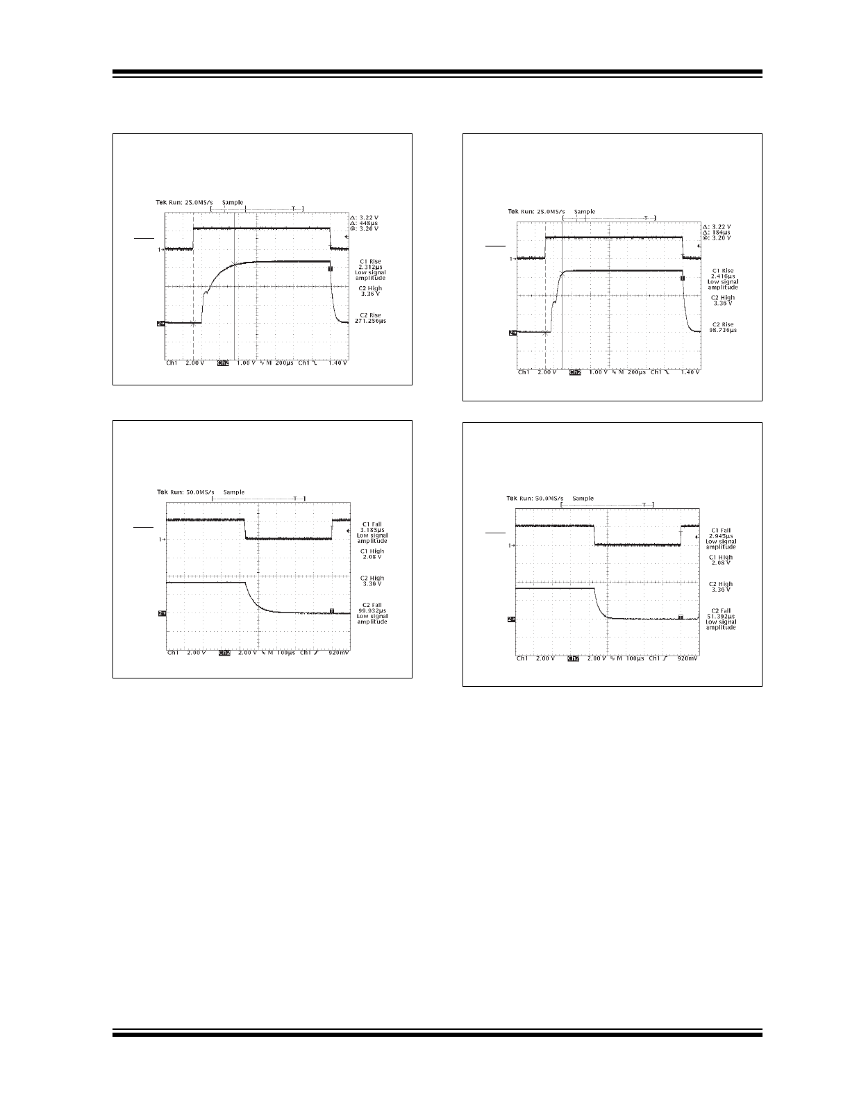
Note: Unless otherwise specified, all parts are measured at temperature = +25°C.
V
OUT
Measure Rise Time of 3.3V LDO with Bypass Capacitor
Conditions: C
IN
= 1
μF, C
OUT
= 1
μF, C
BYP
= 470pF, I
LOAD
= 100mA
V
IN
= 4.3V, Temp = 25
°C, Rise Time = 448μS
V
SHDN
Measure Fall Time of 3.3V LDO with Bypass Capacitor
Conditions: C
IN
= 1
μF, C
OUT
= 1
μF, C
BYP
= 470pF, I
LOAD
= 50mA
V
IN
= 4.3V, Temp = 25
°C, Fall Time = 100μS
V
OUT
V
SHDN
Measure Rise Time of 3.3V LDO without Bypass Capacitor
Conditions: C
IN
= 1
μF, C
OUT
= 1
μF, C
BYP
= 0pF, I
LOAD
= 100mA
V
IN
= 4.3V, Temp = 25
°C, Rise Time = 184μS
V
OUT
V
SHDN
Measure Fall Time of 3.3V LDO without Bypass Capacitor
Conditions: C
IN
= 1
μF, C
OUT
= 1
μF, C
BYP
= 0pF, I
LOAD
= 100mA
V
IN
= 4.3V, Temp = 25
°C, Fall Time = 52μS
V
OUT
V
SHDN
TC1072/TC1073
DS21354D-page 8
© 2007 Microchip Technology Inc.
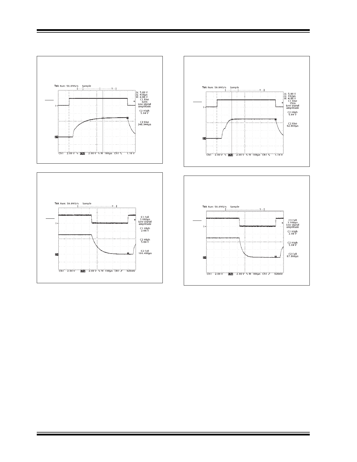
Note: Unless otherwise specified, all parts are measured at temperature = +25°C.
Measure Rise Time of 5.0V LDO with Bypass Capacitor
Conditions: C
IN
= 1
μF, C
OUT
= 1
μF, C
BYP
= 470pF, I
LOAD
= 100mA
V
IN
= 6V, Temp = 25
°C, Rise Time = 390μS
V
OUT
V
SHDN
Measure Fall Time of 5.0V LDO with Bypass Capacitor
Conditions: C
IN
= 1
μF, C
OUT
= 1
μF, C
BYP
= 470pF, I
LOAD
= 50mA
V
IN
= 6V, Temp = 25
°C, Fall Time = 167μS
V
OUT
V
SHDN
Measure Rise Time of 5.0V LDO without Bypass Capacitor
Conditions: C
IN
= 1
μF, C
OUT
= 1
μF, C
BYP
= 0pF, I
LOAD
= 100mA
V
IN
= 6V, Temp = 25
°C, Rise Time = 192μS
V
OUT
V
SHDN
Measure Fall Time of 5.0V LDO without Bypass Capacitor
Conditions: C
IN
= 1
μF, C
OUT
= 1
μF, C
BYP
= 0pF, I
LOAD
= 100mA
V
IN
= 6V, Temp = 25
°C, Fall Time = 88μS
V
OUT
V
SHDN
© 2007 Microchip Technology Inc.
DS21354D-page 9
TC1072/TC1073
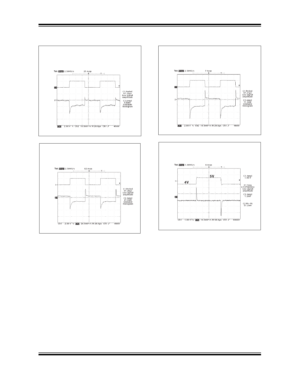
Note: Unless otherwise specified, all parts are measured at temperature = +25°C.
I
LOAD
V
OUT
Load Regulation of 3.3V LDO
Conditions: C
IN
= 1
μF, C
OUT
= 2.2
μF, C
BYP
= 470pF,
V
IN
= V
OUT
+ 0.25V, Temp = 25
°C
I
LOAD
= 50mA switched in at 10kHz, V
OUT
is AC coupled
Load Regulation of 3.3V LDO
Conditions: C
IN
= 1
μF, C
OUT
= 2.2
μF, C
BYP
= 470pF,
V
IN
= V
OUT
+ 0.25V, Temp = 25
°C
I
LOAD
= 150mA switched in at 10kHz, V
OUT
is AC coupled
I
LOAD
V
OUT
Load Regulation of 3.3V LDO
Conditions: C
IN
= 1
μF, C
OUT
= 2.2
μF, C
BYP
= 470pF,
V
IN
= V
OUT
+ 0.25V, Temp = 25
°C
I
LOAD
= 100mA switched in at 10kHz, V
OUT
is AC coupled
I
LOAD
V
OUT
V
IN
V
OUT
Line Regulation of 3.3V LDO
Conditions: V
IN
= 4V, + 1V Squarewave @ 2.5kHz
C
IN
= 0
μF, C
OUT
= 1
μF, C
BYP
= 470pF,
I
LOAD
= 100mA, V
IN
& V
OUT
are AC coupled
TC1072/TC1073
DS21354D-page 10
© 2007 Microchip Technology Inc.
Note: Unless otherwise specified, all parts are measured at temperature = +25°C.
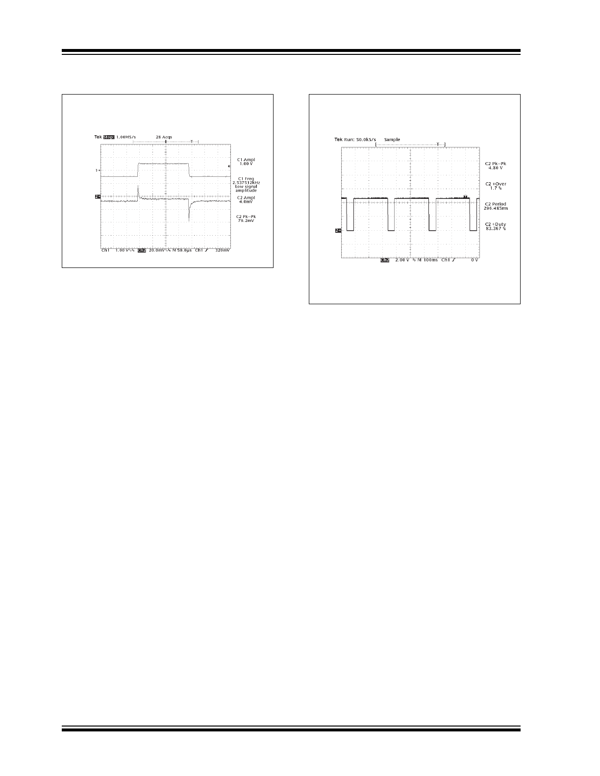
Line Regulation of 5.0V LDO
Conditions: V
IN
= 6V, + 1V Squarewave @ 2.5kHz
V
IN
V
OUT
C
IN
= 0
μF, C
OUT
= 1
μF, C
BYP
= 470pF,
I
LOAD
= 100mA, V
IN
& V
OUT
are AC coupled
V
OUT
Thermal Shutdown Response of 5.0V LDO
Conditions: V
IN
= 6V, C
IN
= 0
μF, C
OUT
= 1
μF
I
LOAD
was increased until temperature of die reached about 160
°C, at
which time integrated thermal protection circuitry shuts the regulator
off when die temperature exceeds approximately 160
°C. The regulator
remains off until die temperature drops to approximately 150
°C.