
2010 Microchip Technology Inc.
DS21353E-page 1
TC1070/TC1071/TC1187
Features:
• 50 µA Ground Current for Longer Battery Life
• Adjustable Output Voltage
• Very Low Dropout Voltage
• Choice of 50 mA (TC1070), 100 mA (TC1071)
and 150 mA (TC1187) Output
• Power-Saving Shutdown mode
• Overcurrent and Overtemperature Protection
• Space-Saving 5-Pin SOT-23 Package
• Pin Compatible with Bipolar Regulators
Applications:
• Battery Operated Systems
• Portable Computers
• Medical Instruments
• Instrumentation
• Cellular/GSM/PHS Phones
• Linear Post-Regulators for SMPS
• Pagers
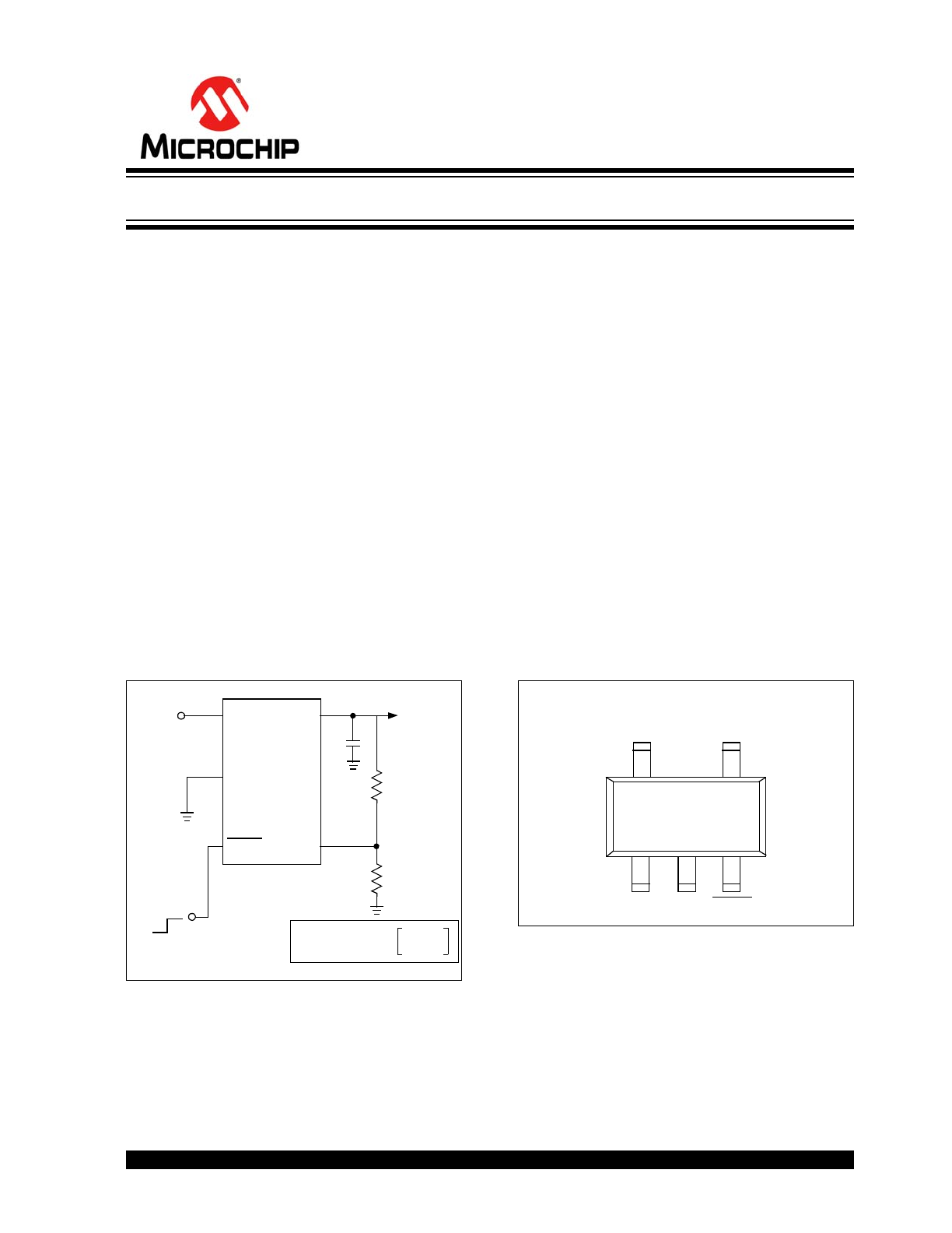
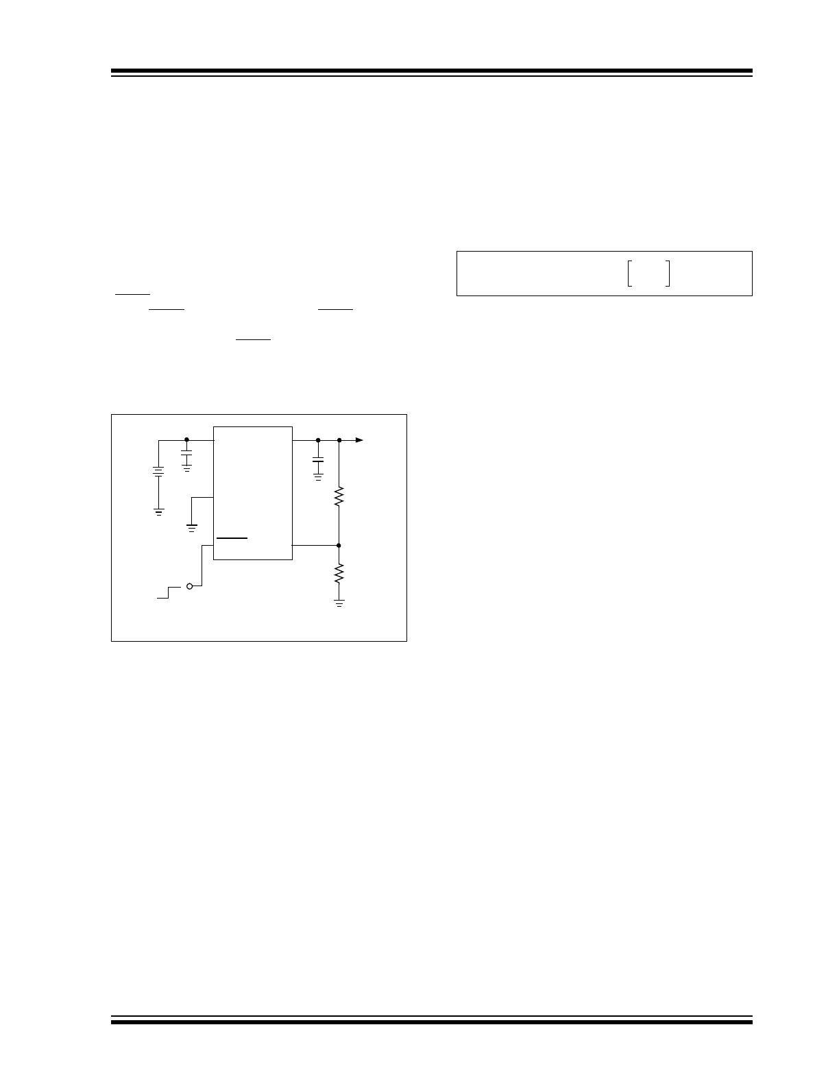
Typical Application
Description:
The TC1070, TC1071 and TC1187 devices are
adjustable LDOs designed to supersede a variety of
older (bipolar) voltage regulators. Total supply current
is typically 50 µA at full load (20 to 60 times lower than
in bipolar regulators).
The devices’ key features include ultra low-noise
operation, very low dropout voltage – typically 85 mV
(TC1070), 180 mV (TC1071) and 270 mV (TC1187) at
full load and fast response to step changes in load.
Supply current is reduced to 0.5 µA (maximum) when
the shutdown input is low. The devices incorporate both
overtemperature and overcurrent protection. Output
voltage is programmed with a simple resistor divider
from V
OUT
to ADJ to GND.
The TC1070, TC1071 and TC1187 devices are stable
with an output capacitor of only 1 µF and have a
maximum output current of 50 mA, 100 mA and
150 mA, respectively. For higher output versions
please see the TC1174 (I
OUT
= 300 mA) data sheet
(DS21363).
Package Type
TC1070
TC1071
TC1187
V
OUT
GND
C1
1 µF
+
V
IN
V
IN
V
OUT
1
5
2
4
3
SHDN
Shutdown Control
(from Power Control Logic)
ADJ
R1
R2
V
OUT
V
REF
R1
R2
-------
1
+
=
ADJ
SHDN
5
5-Pin SOT-23
TC1070
TC1071
TC1187
1
3
4
2
V
IN
V
OUT
GND
50 mA, 100 mA and 150 mA Adjustable CMOS LDOs with Shutdown
TC1070/TC1071/TC1187
DS21353E-page 2
2010 Microchip Technology Inc.
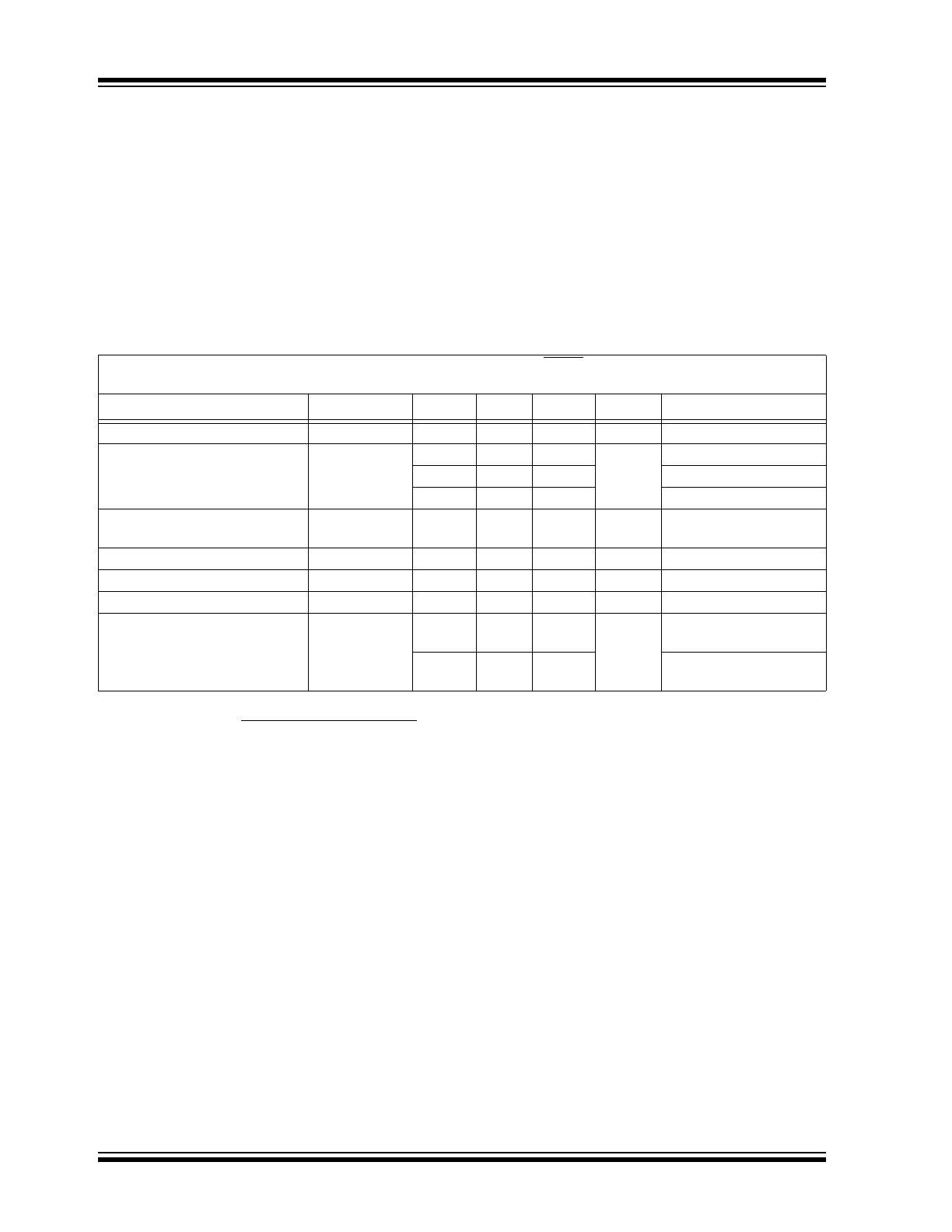
1.0
ELECTRICAL
CHARACTERISTICS
Absolute Maximum Ratings†
Input Voltage .........................................................6.5V
Output Voltage........................... (-0.3V) to (V
IN
+ 0.3V)
Power Dissipation................Internally Limited (
Note 5
)
Maximum Voltage on Any Pin ........ V
IN
+0.3V to -0.3V
Operating Temperature Range...... -40°C < T
J
< 125°C
Storage Temperature..........................-65°C to +150°C
† Notice: Stresses above those listed under "Absolute
Maximum Ratings" may cause permanent damage to
the device. These are stress ratings only and functional
operation of the device at these or any other conditions
above those indicated in the operation sections of the
specifications is not implied. Exposure to Absolute
Maximum Rating conditions for extended periods may
affect device reliability.
ELECTRICAL SPECIFICATIONS
Electrical Characteristics: V
IN
= V
OUT
+ 1V, I
L
= 0.1 mA, C
L
= 3.3 µF, SHDN > V
IH
, T
A
= +25°C, unless otherwise
noted. Boldface type specifications apply for junction temperatures of -40°C to +125°C.
Parameter
Symbol
Min
Typ
Max
Units
Test Conditions
Input Operating Voltage
V
IN
2.7
—
6.0
V
Note 6
Maximum Output Current
I
OUTmax
50
—
—
mA
TC1070
100
—
—
TC1071
150
—
—
TC1187
Adjustable Output
Voltage Range
V
OUT
V
REF
—
5.5
V
Reference Voltage
V
REF
1.165
1.20
1.235
V
V
REF
Temperature Coefficient
V
REF
/
T
—
40
—
ppm/°C
Note 1
Line Regulation
V
OUT
/
V
IN
—
0.05
0.35
%
(V
R
+ 1V)
V
IN
6V
Load Regulation (
Note 2
)
V
OUT
/V
OUT
—
0.5
2
%
TC1070, TC1071
I
L
= 0.1 mA to I
OUTmax
—
0.5
3
TC1187
I
L
= 0.1 mA to I
OUTmax
Note 1:
2:
Regulation is measured at a constant junction temperature using low duty cycle pulse testing. Load regu-
lation is tested over a load range from 0.1 mA to the maximum specified output current. Changes in output
voltage due to heating effects are covered by the thermal regulation specification.
3:
Dropout voltage is defined as the input to output differential at which the output voltage drops 2% below its
nominal value.
4:
Thermal Regulation is defined as the change in output voltage at a time T after a change in power dissipa-
tion is applied, excluding load or line regulation effects. Specifications are for a current pulse equal to
Ilmax at V
IN
= 6V for T = 10 ms.
5:
The maximum allowable power dissipation is a function of ambient temperature, the maximum allowable
junction temperature and the thermal resistance from junction-to-air (i.e., Ta, Tj,
ja). Exceeding the maxi-
mum allowable power dissipation causes the device to initiate thermal shutdown. Please see
Section 5.0
“Thermal Considerations”
for more details.
6:
The minimum VIN has to justify the conditions: V
IN
V
R
+ V
DROPOUT
and V
IN
2.7V for I
L
= 0.1 mA to
I
OUTMAX
.
TC V
OUT
= (V
OUTmax
– V
OUT
MIN
) x 10
6
V
OUT
x
T
2010 Microchip Technology Inc.
DS21353E-page 3
TC1070/TC1071/TC1187
TERMPERATURE CHARACTERISTICS
Dropout Voltage (
Note 3
)
V
IN
-V
OUT
—
2
—
mV
I
L
= 0.1 mA
—
65
—
I
L
= 20 mA
—
85
120
I
L
= 50 mA
—
180
250
TC1071, TC1187
I
L
= 100 mA
—
270
400
TC1187
I
L
= 150 mA
Supply Current
I
IN
—
50
80
µA
SHDN = V
IH
,
I
L
= 0
Shutdown Supply Current
I
INSD
—
0.05
0.5
µA
SHDN =
0V
Power Supply Rejection Ratio
PSRR
—
64
—
dB
F
RE
1 kHz
Output Short Circuit Current
I
OUTSC
—
300
450
mA
V
OUT
= 0V
Thermal Regulation
V
OUT
/
P
D
—
0.04
—
V/W
Note 4
Thermal Shutdown
Die Temperature
T
SD
—
160
—
°C
Thermal Shutdown Hysteresis
T
SD
—
10
—
°C
Output Noise
eN
—
260
—
nV/
Hz I
L
=
I
OUTmax
SHDN Input
SHDN Input High Threshold
V
IH
45
—
—
%V
IN
V
IN
=
2.5V to 6.5V
SHDN Input Low Threshold
V
IL
—
—
15
%V
IN
V
IN
=
2.5V to 6.5
V
ADJ Input
Adjust Input Leakage Current
I
ADJ
—
50
—
pA
Parameters
Sym
Min
Typ
Max
Units
Conditions
Thermal Resistance, 5L-SOT-23
JA
—
256
—
°C/W
ELECTRICAL SPECIFICATIONS (CONTINUED)
Electrical Characteristics: V
IN
= V
OUT
+ 1V, I
L
= 0.1 mA, C
L
= 3.3 µF, SHDN > V
IH
, T
A
= +25°C, unless otherwise
noted. Boldface type specifications apply for junction temperatures of -40°C to +125°C.
Parameter
Symbol
Min
Typ
Max
Units
Test Conditions
Note 1:
2:
Regulation is measured at a constant junction temperature using low duty cycle pulse testing. Load regu-
lation is tested over a load range from 0.1 mA to the maximum specified output current. Changes in output
voltage due to heating effects are covered by the thermal regulation specification.
3:
Dropout voltage is defined as the input to output differential at which the output voltage drops 2% below its
nominal value.
4:
Thermal Regulation is defined as the change in output voltage at a time T after a change in power dissipa-
tion is applied, excluding load or line regulation effects. Specifications are for a current pulse equal to
Ilmax at V
IN
= 6V for T = 10 ms.
5:
The maximum allowable power dissipation is a function of ambient temperature, the maximum allowable
junction temperature and the thermal resistance from junction-to-air (i.e., Ta, Tj,
ja). Exceeding the maxi-
mum allowable power dissipation causes the device to initiate thermal shutdown. Please see
Section 5.0
“Thermal Considerations”
for more details.
6:
The minimum VIN has to justify the conditions: V
IN
V
R
+ V
DROPOUT
and V
IN
2.7V for I
L
= 0.1 mA to
I
OUTMAX
.
TC V
OUT
= (V
OUTmax
– V
OUT
MIN
) x 10
6
V
OUT
x
T
TC1070/TC1071/TC1187
DS21353E-page 4
2010 Microchip Technology Inc.
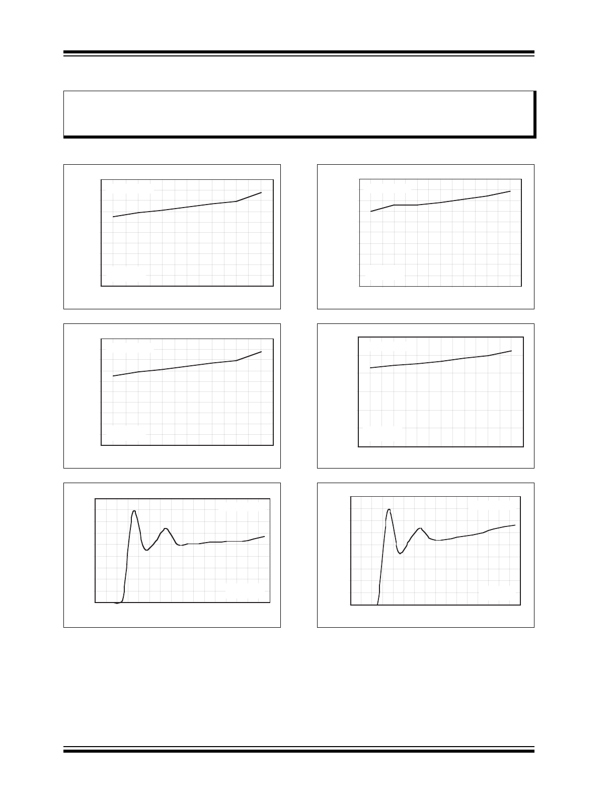
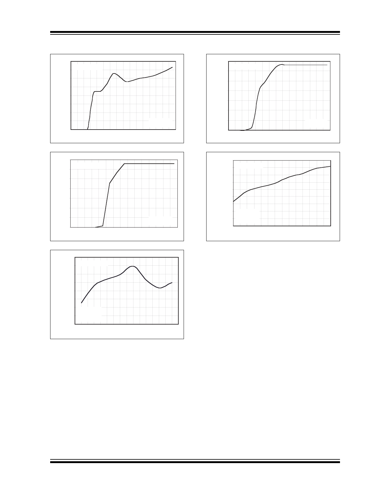
2.0
TYPICAL CHARACTERISTICS
Note: Unless otherwise specified, all parts are measured at temperature = +25°C.
Note:
The graphs and tables provided following this note are a statistical summary based on a limited number of
samples and are provided for informational purposes only. The performance characteristics listed herein
are not tested or guaranteed. In some graphs or tables, the data presented may be outside the specified
operating range (e.g., outside specified power supply range) and therefore outside the warranted range.
0.000
0.002
0.004
0.006
0.008
0.010
0.012
0.014
0.016
0.018
0.020
-40
-20
0
20
50
70
125
DROPOUT VOLTAGE (V)
I
LOAD
= 10mA
C
IN
= 1
μF
C
OUT
= 1
μF
TEMPERATURE (
°C)
Dropout Voltage vs. Temperature (V
OUT
= 3.3V)
0.000
0.002
0.004
0.006
0.008
0.010
0.012
0.014
0.016
0.018
0.020
-40
-20
0
20
50
70
125
DROPOUT VOLTAGE (V)
I
LOAD
= 10mA
C
IN
= 1
μF
C
OUT
= 1
μF
TEMPERATURE (
°C)
Dropout Voltage vs. Temperature (V
OUT
= 3.3V)
0
10
20
30
40
50
60
70
80
90
GND CURRENT (
μ
A)
0 0.5 1 1.5 2 2.5 3 3.5 4 4.5 5 5.5 6 6.5 7 7.5
I
LOAD
= 10mA
C
IN
= 1
μF
C
OUT
= 1
μF
Ground Current vs. V
IN
(V
OUT
= 3.3V)
V
IN
(V)
0.000
0.010
0.020
0.030
0.040
0.050
0.060
0.070
0.080
0.090
0.100
-40
-20
0
20
50
70
125
DROPOUT VOLTAGE (V)
I
LOAD
= 50mA
C
IN
= 1
μF
C
OUT
= 1
μF
TEMPERATURE (
°C)
Dropout Voltage vs. Temperature (V
OUT
= 3.3V)
0.000
0.050
0.100
0.150
0.200
0.250
0.300
-40
-20
0
20
50
70
125
DROPOUT VOLTAGE (V)
I
LOAD
= 150mA
C
IN
= 1
μF
C
OUT
= 1
μF
TEMPERATURE (
°C)
Dropout Voltage vs. Temperature (V
OUT
= 3.3V)
0
10
20
30
40
50
60
70
80
90
GND CURRENT (
μ
A)
0 0.5 1 1.5 2 2.5 3 3.5 4 4.5 5 5.5 6 6.5 7 7.5
I
LOAD
= 100mA
C
IN
= 1
μF
C
OUT
= 1
μF
Ground Current vs. V
IN
(V
OUT
= 3.3V)
V
IN
(V)
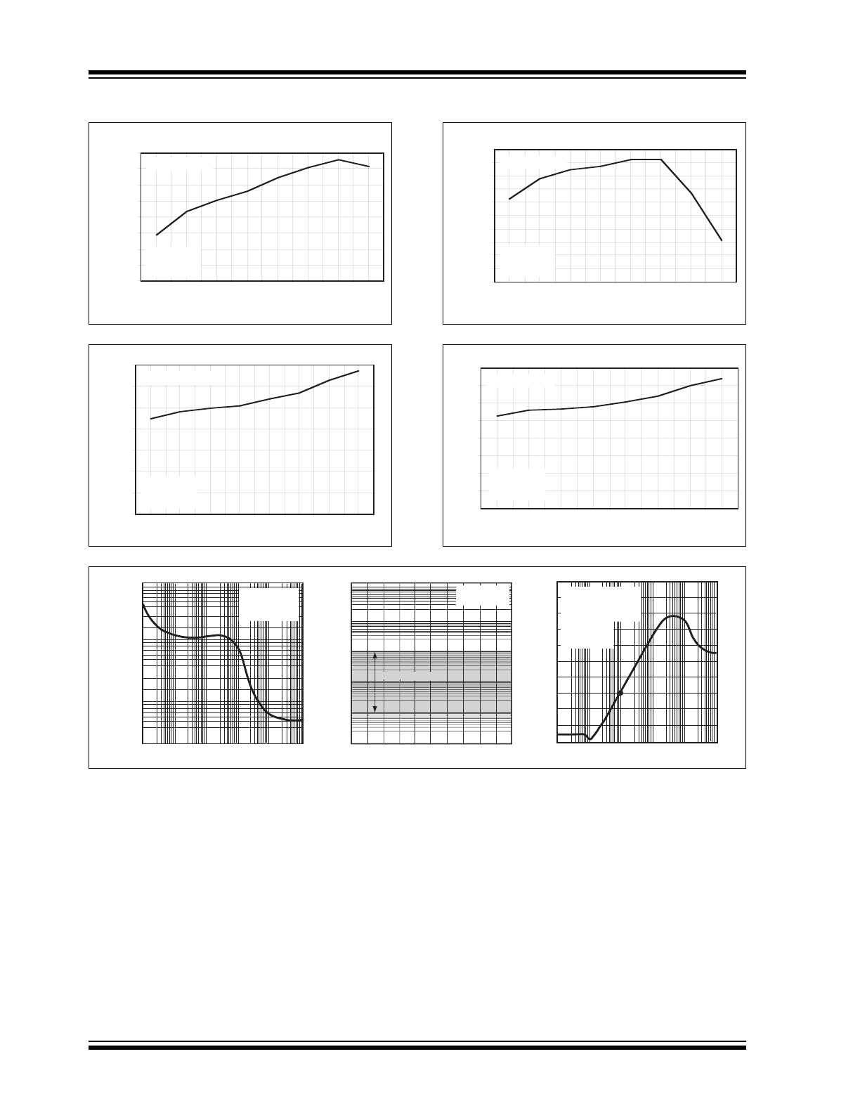
2010 Microchip Technology Inc.
DS21353E-page 5
TC1070/TC1071/TC1187
Note: Unless otherwise specified, all parts are measured at temperature = +25°C.
0
10
20
30
40
50
60
70
80
GND CURRENT (
μ
A)
0 0.5 1 1.5 2 2.5 3 3.5 4 4.5 5 5.5 6 6.5 7 7.5
I
LOAD
= 150mA
C
IN
= 1
μF
C
OUT
= 1
μF
V
IN
(V)
Ground Current vs. V
IN
(V
OUT
= 3.3V)
0.0
0.5
1.0
1.5
2.0
2.5
3.0
3.5
I
LOAD
= 100mA
C
IN
= 1
μF
C
OUT
= 1
μF
0 0.5 1 1.5 2 2.5 3 3.5 4 4.5 5 5.5 6 6.5 7
V
IN
(V)
V
OUT
(V)
V
OUT
vs.
V
IN
(V
OUT
= 3.3V)
3.274
3.276
3.278
3.280
3.282
3.284
3.286
3.288
3.290
-40
-20
-10
0
20
40
85
125
I
LOAD
= 150mA
C
IN
= 1
μF
C
OUT
= 1
μF
V
IN
= 4.3V
TEMPERATURE (
°C)
V
OUT
(V)
Output Voltage vs. Temperature (V
OUT
= 3.3V)
0
0.5
1
1.5
2
2.5
3
3.5
0 0.5 1 1.5 2 2.5 3 3.5 4 4.5 5 5.5 6 6.5 7
I
LOAD
= 0
C
IN
= 1
μF
C
OUT
= 1
μF
V
IN
(V)
V
OUT
(V)
V
OUT
vs.
V
IN
(V
OUT
= 3.3V)
3.275
3.280
3.285
3.290
3.295
3.300
3.305
3.310
3.315
3.320
-40
-20
-10
0
20
40
85
125
I
LOAD
= 10mA
C
IN
= 1
μF
C
OUT
= 1
μF
V
IN
= 4.3V
TEMPERATURE (
°C)
V
OUT
(V)
Output Voltage vs. Temperature (V
OUT
= 3.3V)
TC1070/TC1071/TC1187
DS21353E-page 6
2010 Microchip Technology Inc.
Note: Unless otherwise specified, all parts are measured at temperature = +25°C.
Note: Unless otherwise specified, all parts are measured at temperature = +25°C.
4.985
4.990
4.995
5.000
5.005
5.010
5.015
5.020
5.025
-40
-20
-10
0
20
40
85
125
I
LOAD
= 10mA
V
IN
= 6V
C
IN
= 1
μF
C
OUT
= 1
μF
TEMPERATURE (
°C)
Output Voltage vs. Temperature (V
OUT
= 5V)
V
OUT
(V)
0
10
20
30
40
50
60
70
-40
-20
-10
0
20
40
85
125
GND CURRENT (
μ
A)
I
LOAD
= 10mA
V
IN
= 6V
C
IN
= 1
μF
C
OUT
= 1
μF
TEMPERATURE (
°C)
Temperature
vs. Quiescent Current (V
OUT
= 5V)
4.974
4.976
4.978
4.980
4.982
4.984
4.986
4.988
4.990
4.992
4.994
-40
-20
-10
0
20
40
85
125
I
LOAD
= 150mA
V
IN
= 6V
C
IN
= 1
μF
C
OUT
= 1
μF
TEMPERATURE (
°C)
Output Voltage vs. Temperature (V
OUT
= 5V)
V
OUT
(V)
Temperature vs. Quiescent Current (V
OUT
= 5V)
0
10
20
30
40
50
60
70
80
-40
-20
-10
0
20
40
85
125
GND CURRENT (
μ
A)
I
LOAD
= 150mA
V
IN
= 6V
C
IN
= 1
μF
C
OUT
= 1
μF
TEMPERATURE (
°C)
10.0
1.0
0.1
0.0
0.01K 0.1K
1K
10K
100K
1000K
FREQUENCY (Hz)
Output Noise vs. Frequency
NOISE (
μ
V/
√
Hz)
R
LOAD
= 50
Ω
C
OUT
= 1
μF
C
IN
= 1
μF
1000
100
10
1
0.1
0.01
0
10 20 30 40 50 60 70 80 90 100
LOAD CURRENT (mA)
Stability Region vs. Load Current
C
OUT
ESR
(Ω
)
C
OUT
= 1
μF
to 10
μF
Stable Region
Stable Region
-30
-35
-40
-45
-50
-60
-55
-65
-70
-75
-80
0.01K 0.1K
1K
10K
100K 1000K
FREQUENCY (Hz)
Power Supply Rejection Ratio
PSRR (dB)
I
OUT
=
10mA
V
INDC
=
4V
V
INAC
=
100mVp-p
V
OUT
=
3V
C
IN
=
0
C
OUT
=
1
μF
2010 Microchip Technology Inc.
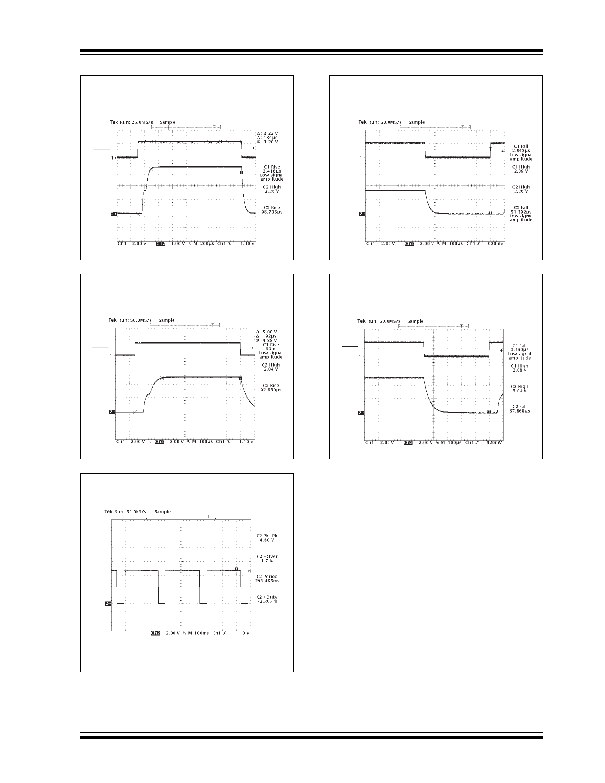
DS21353E-page 7
TC1070/TC1071/TC1187
V
OUT
V
SHDN
Measure Rise Time of 3.3V LDO
Conditions: C
IN
= 1
μF, C
OUT
= 1
μF, I
LOAD
= 100mA, V
IN
= 4.3V,
Temp = 25
°C, Fall Time = 184μS
V
SHDN
Measure Rise Time of 5.0V LDO
Conditions: C
IN
= 1
μF, C
OUT
= 1
μF, I
LOAD
= 100mA, V
IN
= 6V,
Temp = 25
°C, Fall Time = 192μS
V
OUT
Thermal Shutdown Response of 5.0V LDO
Conditions: V
IN
= 6V, C
IN
= 0
μF, C
OUT
= 1
μF
I
LOAD
was increased until temperature of die reached about 160
°C, at
which time integrated thermal protection circuitry shuts the regulator
off when die temperature exceeds approximately 160
°C. The regulator
remains off until die temperature drops to approximately 150
°C.
V
OUT
Measure Fall Time of 3.3V LDO
Conditions: C
IN
= 1
μF, C
OUT
= 1
μF, I
LOAD
= 100mA, V
IN
= 4.3V,
Temp = 25
°C, Fall Time = 52μS
V
OUT
V
SHDN
Measure Fall Time of 5.0V LDO
Conditions: C
IN
= 1
μF, C
OUT
= 1
μF, I
LOAD
= 100mA, V
IN
= 6V,
Temp = 25
°C, Fall Time = 88μS
V
OUT
V
SHDN
TC1070/TC1071/TC1187
DS21353E-page 8
2010 Microchip Technology Inc.
3.0
PIN DESCRIPTIONS
The descriptions of the pins are listed in
Table 3-1
.
3.1
Input Voltage Supply (V
IN
)
Connect unregulated input supply to the V
IN
pin. If
there is a large distance between the input supply and
the LDO regulator, some input capacitance is
necessary for proper operation. A 1 µF capacitor
connected from V
IN
to ground is recommended for
most applications.
3.2
Ground (GND)
Connect the unregulated input supply ground return to
GND. Also connect the negative side of the 1 µF typical
input decoupling capacitor close to GND and the
negative side of the output capacitor C
1
to GND.
3.3
Shutdown Control Input (SHDN)
The regulator is fully enabled when a logic high is
applied to this input. The regulator enters shutdown
when a logic low is applied to this input. During
shutdown, output voltage falls to zero and supply
current is reduced to 0.5 µA (maximum).
3.4
Output Voltage Adjust (ADJ)
Output voltage setting is programmed with a resistor
divider from V
OUT
to this input.
3.5
Regulated Voltage Output (V
OUT
)
Connect the output load to V
OUT
of the LDO. Also
connect the positive side of the LDO output capacitor
as close as possible to the V
OUT
pin.
TABLE 3-1:
PIN FUNCTION TABLE
TC1070/TC1071/TC1187
Symbol
Description
SOT-23
1
V
IN
Unregulated supply input
2
GND
Ground terminal
3
SHDN
Shutdown control input
4
ADJ
Output voltage adjust terminal
5
V
OUT
Regulated voltage output
2010 Microchip Technology Inc.
DS21353E-page 9
TC1070/TC1071/TC1187
4.0
DETAILED DESCRIPTION
The TC1070, TC1071 and TC1187 are adjustable
output voltage regulators. (If a fixed version is desired,
please see the TC1014/TC1015/TC1185 data sheet –
DS21335.) Unlike bipolar regulators, the TC1070,
TC1071 and TC1187 supply current does not increase
with load current. In addition, V
OUT
remains stable and
within regulation over the entire 0 mA to I
OUTmax
oper-
ating load current range (an important consideration in
RTC and CMOS RAM battery back-up applications).
Figure 4-1
shows a typical application circuit. The
regulator is enabled any time the shutdown input
(SHDN) is at or above V
IH
, and shutdown (disabled)
when SHDN is at or below V
IL
. SHDN may be
controlled by a CMOS logic gate or I/O port of a
microcontroller. If the SHDN input is not required, it
should be connected directly to the input supply. While
in shutdown, supply current decreases to 0.05 µA
(typical) and V
OUT
falls to zero volts.
FIGURE 4-1:
Battery-Operated Supply.
4.1
Adjust Input
The output voltage setting is determined by the values
of R
1
and R
2
(see
Equation 4-1
). The ohmic values of
these resistors should be between 470K and 3M to
minimize bleeder current.
The output voltage setting is calculated using the
following equation:
EQUATION 4-1:
The voltage adjustment range of the TC1070, TC1071
and TC1187 is from V
REF
to (V
IN
– 0.05V).
4.2
Output Capacitor
A 1 µF (minimum) capacitor from V
OUT
to ground is
recommended. The output capacitor should have an
effective series resistance greater than 0.1
and less
than 5.0
, and a resonant frequency above 1 MHz.
Aluminum electrolytic or tantalum capacitor types can
be used. (Since many aluminum electrolytic capacitors
freeze at approximately -30°C, solid tantalums are rec-
ommended for applications operating below -25°C.)
When operating from sources other than batteries,
supply-noise rejection and transient response can be
improved by increasing the value of the input and
output capacitors and employing passive filtering
techniques.
4.3
Input Capacitor
A 1 µF capacitor should be connected from V
IN
to
GND if there is more than 10 inches of wire between
the regulator and the AC filter capacitor, or if a battery
is used as power source.
TC1070
TC1071
TC1187
V
OUT
SHDN
GND
C2 +
V
IN
+2.45V
Shutdown Control
(from Power Control Logic)
C1
1 µF
+
3.0V
Battery
+
R1
470K
1
5
2
4
3
ADJ
R2
470K
1 µF
V
OUT
V
REF
R
1
R
2
------
1
=
TC1070/TC1071/TC1187
DS21353E-page 10
2010 Microchip Technology Inc.
5.0
THERMAL CONSIDERATIONS
5.1
Thermal Shutdown
Integrated thermal protection circuitry shuts the
regulator off when die temperature exceeds 160°C.
The regulator remains off until the die temperature
drops to approximately 150°C.
5.2
Power Dissipation
The amount of power the regulator dissipates is
primarily a function of input and output voltage, and
output current. The following equation is used to
calculate worst-case actual power dissipation:
EQUATION 5-1:
The maximum allowable power dissipation
(
Equation 5-2
) is a function of the maximum ambient
temperature (T
Amax
), the maximum allowable die
temperature (T
Jmax
) and the thermal resistance from
junction-to-air (
JA
). The 5-Pin SOT-23 package has a
JA
of approximately 220° C/Watt.
EQUATION 5-2:
Equation 5-1
can be used in conjunction with
Equation 5-2
to ensure regulator thermal operation is
within limits. For example:
Actual power dissipation:
Maximum allowable power dissipation:
In this example, the TC1070 dissipates a maximum of
26.2 mW which is below the allowable limit of 318 mW.
In a similar manner,
Equation 5-1
and
Equation 5-2
can
be used to calculate maximum current and/or input
voltage limits.
5.3
Layout Considerations
The primary path of heat conduction out of the package
is via the package leads. Therefore, layouts having a
ground plane, wide traces at the pads, and wide power
supply bus lines combine to lower
JA
and therefore
increase the maximum allowable power dissipation
limit.
P
D
(V
INmax
– V
OUTmin
)I
LOADmax
Where:
P
D
= Worst-case actual power dissipation
V
INmax
= Maximum voltage on V
IN
V
OUTmin
= Minimum regulator output voltage
I
LOADmax
= Maximum output (load) current
where all terms are previously defined.
P
Dmax
T
Jmax
T
Amax
–
J A
----------------------------------------
=
Given:
V
INmax
=
3.0V ±10%
V
OUTmin
=
2.7V – 2%
I
LOADmax
=
40 mA
T
Jmax
=
+125°C
T
Amax
=
+55°C
Find:
1. Actual power dissipation
2. Maximum allowable dissipation
P
D
(V
INmax
– V
OUTmin
)I
LOADmax
= [(3.0 x 1.10) – (2.7 x .0.98)]40 x 10
–3
= 26.2 mW
= 318 mW
125
55
–
220
-------------------------
=
P
Dmax
T
Jmax
T
Amax
–
JA
----------------------------------------
=
2010 Microchip Technology Inc.
DS21353E-page 1
TC1070/TC1071/TC1187
Features:
• 50 µA Ground Current for Longer Battery Life
• Adjustable Output Voltage
• Very Low Dropout Voltage
• Choice of 50 mA (TC1070), 100 mA (TC1071)
and 150 mA (TC1187) Output
• Power-Saving Shutdown mode
• Overcurrent and Overtemperature Protection
• Space-Saving 5-Pin SOT-23 Package
• Pin Compatible with Bipolar Regulators
Applications:
• Battery Operated Systems
• Portable Computers
• Medical Instruments
• Instrumentation
• Cellular/GSM/PHS Phones
• Linear Post-Regulators for SMPS
• Pagers
Typical Application
Description:
The TC1070, TC1071 and TC1187 devices are
adjustable LDOs designed to supersede a variety of
older (bipolar) voltage regulators. Total supply current
is typically 50 µA at full load (20 to 60 times lower than
in bipolar regulators).
The devices’ key features include ultra low-noise
operation, very low dropout voltage – typically 85 mV
(TC1070), 180 mV (TC1071) and 270 mV (TC1187) at
full load and fast response to step changes in load.
Supply current is reduced to 0.5 µA (maximum) when
the shutdown input is low. The devices incorporate both
overtemperature and overcurrent protection. Output
voltage is programmed with a simple resistor divider
from V
OUT
to ADJ to GND.
The TC1070, TC1071 and TC1187 devices are stable
with an output capacitor of only 1 µF and have a
maximum output current of 50 mA, 100 mA and
150 mA, respectively. For higher output versions
please see the TC1174 (I
OUT
= 300 mA) data sheet
(DS21363).
Package Type
TC1070
TC1071
TC1187
V
OUT
GND
C1
1 µF
+
V
IN
V
IN
V
OUT
1
5
2
4
3
SHDN
Shutdown Control
(from Power Control Logic)
ADJ
R1
R2
V
OUT
V
REF
R1
R2
-------
1
+
=
ADJ
SHDN
5
5-Pin SOT-23
TC1070
TC1071
TC1187
1
3
4
2
V
IN
V
OUT
GND
50 mA, 100 mA and 150 mA Adjustable CMOS LDOs with Shutdown
TC1070/TC1071/TC1187
DS21353E-page 2
2010 Microchip Technology Inc.
1.0
ELECTRICAL
CHARACTERISTICS
Absolute Maximum Ratings†
Input Voltage .........................................................6.5V
Output Voltage........................... (-0.3V) to (V
IN
+ 0.3V)
Power Dissipation................Internally Limited (
Note 5
)
Maximum Voltage on Any Pin ........ V
IN
+0.3V to -0.3V
Operating Temperature Range...... -40°C < T
J
< 125°C
Storage Temperature..........................-65°C to +150°C
† Notice: Stresses above those listed under "Absolute
Maximum Ratings" may cause permanent damage to
the device. These are stress ratings only and functional
operation of the device at these or any other conditions
above those indicated in the operation sections of the
specifications is not implied. Exposure to Absolute
Maximum Rating conditions for extended periods may
affect device reliability.
ELECTRICAL SPECIFICATIONS
Electrical Characteristics: V
IN
= V
OUT
+ 1V, I
L
= 0.1 mA, C
L
= 3.3 µF, SHDN > V
IH
, T
A
= +25°C, unless otherwise
noted. Boldface type specifications apply for junction temperatures of -40°C to +125°C.
Parameter
Symbol
Min
Typ
Max
Units
Test Conditions
Input Operating Voltage
V
IN
2.7
—
6.0
V
Note 6
Maximum Output Current
I
OUTmax
50
—
—
mA
TC1070
100
—
—
TC1071
150
—
—
TC1187
Adjustable Output
Voltage Range
V
OUT
V
REF
—
5.5
V
Reference Voltage
V
REF
1.165
1.20
1.235
V
V
REF
Temperature Coefficient
V
REF
/
T
—
40
—
ppm/°C
Note 1
Line Regulation
V
OUT
/
V
IN
—
0.05
0.35
%
(V
R
+ 1V)
V
IN
6V
Load Regulation (
Note 2
)
V
OUT
/V
OUT
—
0.5
2
%
TC1070, TC1071
I
L
= 0.1 mA to I
OUTmax
—
0.5
3
TC1187
I
L
= 0.1 mA to I
OUTmax
Note 1:
2:
Regulation is measured at a constant junction temperature using low duty cycle pulse testing. Load regu-
lation is tested over a load range from 0.1 mA to the maximum specified output current. Changes in output
voltage due to heating effects are covered by the thermal regulation specification.
3:
Dropout voltage is defined as the input to output differential at which the output voltage drops 2% below its
nominal value.
4:
Thermal Regulation is defined as the change in output voltage at a time T after a change in power dissipa-
tion is applied, excluding load or line regulation effects. Specifications are for a current pulse equal to
Ilmax at V
IN
= 6V for T = 10 ms.
5:
The maximum allowable power dissipation is a function of ambient temperature, the maximum allowable
junction temperature and the thermal resistance from junction-to-air (i.e., Ta, Tj,
ja). Exceeding the maxi-
mum allowable power dissipation causes the device to initiate thermal shutdown. Please see
Section 5.0
“Thermal Considerations”
for more details.
6:
The minimum VIN has to justify the conditions: V
IN
V
R
+ V
DROPOUT
and V
IN
2.7V for I
L
= 0.1 mA to
I
OUTMAX
.
TC V
OUT
= (V
OUTmax
– V
OUT
MIN
) x 10
6
V
OUT
x
T
2010 Microchip Technology Inc.
DS21353E-page 3
TC1070/TC1071/TC1187
TERMPERATURE CHARACTERISTICS
Dropout Voltage (
Note 3
)
V
IN
-V
OUT
—
2
—
mV
I
L
= 0.1 mA
—
65
—
I
L
= 20 mA
—
85
120
I
L
= 50 mA
—
180
250
TC1071, TC1187
I
L
= 100 mA
—
270
400
TC1187
I
L
= 150 mA
Supply Current
I
IN
—
50
80
µA
SHDN = V
IH
,
I
L
= 0
Shutdown Supply Current
I
INSD
—
0.05
0.5
µA
SHDN =
0V
Power Supply Rejection Ratio
PSRR
—
64
—
dB
F
RE
1 kHz
Output Short Circuit Current
I
OUTSC
—
300
450
mA
V
OUT
= 0V
Thermal Regulation
V
OUT
/
P
D
—
0.04
—
V/W
Note 4
Thermal Shutdown
Die Temperature
T
SD
—
160
—
°C
Thermal Shutdown Hysteresis
T
SD
—
10
—
°C
Output Noise
eN
—
260
—
nV/
Hz I
L
=
I
OUTmax
SHDN Input
SHDN Input High Threshold
V
IH
45
—
—
%V
IN
V
IN
=
2.5V to 6.5V
SHDN Input Low Threshold
V
IL
—
—
15
%V
IN
V
IN
=
2.5V to 6.5
V
ADJ Input
Adjust Input Leakage Current
I
ADJ
—
50
—
pA
Parameters
Sym
Min
Typ
Max
Units
Conditions
Thermal Resistance, 5L-SOT-23
JA
—
256
—
°C/W
ELECTRICAL SPECIFICATIONS (CONTINUED)
Electrical Characteristics: V
IN
= V
OUT
+ 1V, I
L
= 0.1 mA, C
L
= 3.3 µF, SHDN > V
IH
, T
A
= +25°C, unless otherwise
noted. Boldface type specifications apply for junction temperatures of -40°C to +125°C.
Parameter
Symbol
Min
Typ
Max
Units
Test Conditions
Note 1:
2:
Regulation is measured at a constant junction temperature using low duty cycle pulse testing. Load regu-
lation is tested over a load range from 0.1 mA to the maximum specified output current. Changes in output
voltage due to heating effects are covered by the thermal regulation specification.
3:
Dropout voltage is defined as the input to output differential at which the output voltage drops 2% below its
nominal value.
4:
Thermal Regulation is defined as the change in output voltage at a time T after a change in power dissipa-
tion is applied, excluding load or line regulation effects. Specifications are for a current pulse equal to
Ilmax at V
IN
= 6V for T = 10 ms.
5:
The maximum allowable power dissipation is a function of ambient temperature, the maximum allowable
junction temperature and the thermal resistance from junction-to-air (i.e., Ta, Tj,
ja). Exceeding the maxi-
mum allowable power dissipation causes the device to initiate thermal shutdown. Please see
Section 5.0
“Thermal Considerations”
for more details.
6:
The minimum VIN has to justify the conditions: V
IN
V
R
+ V
DROPOUT
and V
IN
2.7V for I
L
= 0.1 mA to
I
OUTMAX
.
TC V
OUT
= (V
OUTmax
– V
OUT
MIN
) x 10
6
V
OUT
x
T
TC1070/TC1071/TC1187
DS21353E-page 4
2010 Microchip Technology Inc.
2.0
TYPICAL CHARACTERISTICS
Note: Unless otherwise specified, all parts are measured at temperature = +25°C.
Note:
The graphs and tables provided following this note are a statistical summary based on a limited number of
samples and are provided for informational purposes only. The performance characteristics listed herein
are not tested or guaranteed. In some graphs or tables, the data presented may be outside the specified
operating range (e.g., outside specified power supply range) and therefore outside the warranted range.
0.000
0.002
0.004
0.006
0.008
0.010
0.012
0.014
0.016
0.018
0.020
-40
-20
0
20
50
70
125
DROPOUT VOLTAGE (V)
I
LOAD
= 10mA
C
IN
= 1
μF
C
OUT
= 1
μF
TEMPERATURE (
°C)
Dropout Voltage vs. Temperature (V
OUT
= 3.3V)
0.000
0.002
0.004
0.006
0.008
0.010
0.012
0.014
0.016
0.018
0.020
-40
-20
0
20
50
70
125
DROPOUT VOLTAGE (V)
I
LOAD
= 10mA
C
IN
= 1
μF
C
OUT
= 1
μF
TEMPERATURE (
°C)
Dropout Voltage vs. Temperature (V
OUT
= 3.3V)
0
10
20
30
40
50
60
70
80
90
GND CURRENT (
μ
A)
0 0.5 1 1.5 2 2.5 3 3.5 4 4.5 5 5.5 6 6.5 7 7.5
I
LOAD
= 10mA
C
IN
= 1
μF
C
OUT
= 1
μF
Ground Current vs. V
IN
(V
OUT
= 3.3V)
V
IN
(V)
0.000
0.010
0.020
0.030
0.040
0.050
0.060
0.070
0.080
0.090
0.100
-40
-20
0
20
50
70
125
DROPOUT VOLTAGE (V)
I
LOAD
= 50mA
C
IN
= 1
μF
C
OUT
= 1
μF
TEMPERATURE (
°C)
Dropout Voltage vs. Temperature (V
OUT
= 3.3V)
0.000
0.050
0.100
0.150
0.200
0.250
0.300
-40
-20
0
20
50
70
125
DROPOUT VOLTAGE (V)
I
LOAD
= 150mA
C
IN
= 1
μF
C
OUT
= 1
μF
TEMPERATURE (
°C)
Dropout Voltage vs. Temperature (V
OUT
= 3.3V)
0
10
20
30
40
50
60
70
80
90
GND CURRENT (
μ
A)
0 0.5 1 1.5 2 2.5 3 3.5 4 4.5 5 5.5 6 6.5 7 7.5
I
LOAD
= 100mA
C
IN
= 1
μF
C
OUT
= 1
μF
Ground Current vs. V
IN
(V
OUT
= 3.3V)
V
IN
(V)
2010 Microchip Technology Inc.
DS21353E-page 5
TC1070/TC1071/TC1187
Note: Unless otherwise specified, all parts are measured at temperature = +25°C.
0
10
20
30
40
50
60
70
80
GND CURRENT (
μ
A)
0 0.5 1 1.5 2 2.5 3 3.5 4 4.5 5 5.5 6 6.5 7 7.5
I
LOAD
= 150mA
C
IN
= 1
μF
C
OUT
= 1
μF
V
IN
(V)
Ground Current vs. V
IN
(V
OUT
= 3.3V)
0.0
0.5
1.0
1.5
2.0
2.5
3.0
3.5
I
LOAD
= 100mA
C
IN
= 1
μF
C
OUT
= 1
μF
0 0.5 1 1.5 2 2.5 3 3.5 4 4.5 5 5.5 6 6.5 7
V
IN
(V)
V
OUT
(V)
V
OUT
vs.
V
IN
(V
OUT
= 3.3V)
3.274
3.276
3.278
3.280
3.282
3.284
3.286
3.288
3.290
-40
-20
-10
0
20
40
85
125
I
LOAD
= 150mA
C
IN
= 1
μF
C
OUT
= 1
μF
V
IN
= 4.3V
TEMPERATURE (
°C)
V
OUT
(V)
Output Voltage vs. Temperature (V
OUT
= 3.3V)
0
0.5
1
1.5
2
2.5
3
3.5
0 0.5 1 1.5 2 2.5 3 3.5 4 4.5 5 5.5 6 6.5 7
I
LOAD
= 0
C
IN
= 1
μF
C
OUT
= 1
μF
V
IN
(V)
V
OUT
(V)
V
OUT
vs.
V
IN
(V
OUT
= 3.3V)
3.275
3.280
3.285
3.290
3.295
3.300
3.305
3.310
3.315
3.320
-40
-20
-10
0
20
40
85
125
I
LOAD
= 10mA
C
IN
= 1
μF
C
OUT
= 1
μF
V
IN
= 4.3V
TEMPERATURE (
°C)
V
OUT
(V)
Output Voltage vs. Temperature (V
OUT
= 3.3V)
TC1070/TC1071/TC1187
DS21353E-page 6
2010 Microchip Technology Inc.
Note: Unless otherwise specified, all parts are measured at temperature = +25°C.
Note: Unless otherwise specified, all parts are measured at temperature = +25°C.
4.985
4.990
4.995
5.000
5.005
5.010
5.015
5.020
5.025
-40
-20
-10
0
20
40
85
125
I
LOAD
= 10mA
V
IN
= 6V
C
IN
= 1
μF
C
OUT
= 1
μF
TEMPERATURE (
°C)
Output Voltage vs. Temperature (V
OUT
= 5V)
V
OUT
(V)
0
10
20
30
40
50
60
70
-40
-20
-10
0
20
40
85
125
GND CURRENT (
μ
A)
I
LOAD
= 10mA
V
IN
= 6V
C
IN
= 1
μF
C
OUT
= 1
μF
TEMPERATURE (
°C)
Temperature
vs. Quiescent Current (V
OUT
= 5V)
4.974
4.976
4.978
4.980
4.982
4.984
4.986
4.988
4.990
4.992
4.994
-40
-20
-10
0
20
40
85
125
I
LOAD
= 150mA
V
IN
= 6V
C
IN
= 1
μF
C
OUT
= 1
μF
TEMPERATURE (
°C)
Output Voltage vs. Temperature (V
OUT
= 5V)
V
OUT
(V)
Temperature vs. Quiescent Current (V
OUT
= 5V)
0
10
20
30
40
50
60
70
80
-40
-20
-10
0
20
40
85
125
GND CURRENT (
μ
A)
I
LOAD
= 150mA
V
IN
= 6V
C
IN
= 1
μF
C
OUT
= 1
μF
TEMPERATURE (
°C)
10.0
1.0
0.1
0.0
0.01K 0.1K
1K
10K
100K
1000K
FREQUENCY (Hz)
Output Noise vs. Frequency
NOISE (
μ
V/
√
Hz)
R
LOAD
= 50
Ω
C
OUT
= 1
μF
C
IN
= 1
μF
1000
100
10
1
0.1
0.01
0
10 20 30 40 50 60 70 80 90 100
LOAD CURRENT (mA)
Stability Region vs. Load Current
C
OUT
ESR
(Ω
)
C
OUT
= 1
μF
to 10
μF
Stable Region
Stable Region
-30
-35
-40
-45
-50
-60
-55
-65
-70
-75
-80
0.01K 0.1K
1K
10K
100K 1000K
FREQUENCY (Hz)
Power Supply Rejection Ratio
PSRR (dB)
I
OUT
=
10mA
V
INDC
=
4V
V
INAC
=
100mVp-p
V
OUT
=
3V
C
IN
=
0
C
OUT
=
1
μF
2010 Microchip Technology Inc.
DS21353E-page 7
TC1070/TC1071/TC1187
V
OUT
V
SHDN
Measure Rise Time of 3.3V LDO
Conditions: C
IN
= 1
μF, C
OUT
= 1
μF, I
LOAD
= 100mA, V
IN
= 4.3V,
Temp = 25
°C, Fall Time = 184μS
V
SHDN
Measure Rise Time of 5.0V LDO
Conditions: C
IN
= 1
μF, C
OUT
= 1
μF, I
LOAD
= 100mA, V
IN
= 6V,
Temp = 25
°C, Fall Time = 192μS
V
OUT
Thermal Shutdown Response of 5.0V LDO
Conditions: V
IN
= 6V, C
IN
= 0
μF, C
OUT
= 1
μF
I
LOAD
was increased until temperature of die reached about 160
°C, at
which time integrated thermal protection circuitry shuts the regulator
off when die temperature exceeds approximately 160
°C. The regulator
remains off until die temperature drops to approximately 150
°C.
V
OUT
Measure Fall Time of 3.3V LDO
Conditions: C
IN
= 1
μF, C
OUT
= 1
μF, I
LOAD
= 100mA, V
IN
= 4.3V,
Temp = 25
°C, Fall Time = 52μS
V
OUT
V
SHDN
Measure Fall Time of 5.0V LDO
Conditions: C
IN
= 1
μF, C
OUT
= 1
μF, I
LOAD
= 100mA, V
IN
= 6V,
Temp = 25
°C, Fall Time = 88μS
V
OUT
V
SHDN
TC1070/TC1071/TC1187
DS21353E-page 8
2010 Microchip Technology Inc.
3.0
PIN DESCRIPTIONS
The descriptions of the pins are listed in
Table 3-1
.
3.1
Input Voltage Supply (V
IN
)
Connect unregulated input supply to the V
IN
pin. If
there is a large distance between the input supply and
the LDO regulator, some input capacitance is
necessary for proper operation. A 1 µF capacitor
connected from V
IN
to ground is recommended for
most applications.
3.2
Ground (GND)
Connect the unregulated input supply ground return to
GND. Also connect the negative side of the 1 µF typical
input decoupling capacitor close to GND and the
negative side of the output capacitor C
1
to GND.
3.3
Shutdown Control Input (SHDN)
The regulator is fully enabled when a logic high is
applied to this input. The regulator enters shutdown
when a logic low is applied to this input. During
shutdown, output voltage falls to zero and supply
current is reduced to 0.5 µA (maximum).
3.4
Output Voltage Adjust (ADJ)
Output voltage setting is programmed with a resistor
divider from V
OUT
to this input.
3.5
Regulated Voltage Output (V
OUT
)
Connect the output load to V
OUT
of the LDO. Also
connect the positive side of the LDO output capacitor
as close as possible to the V
OUT
pin.
TABLE 3-1:
PIN FUNCTION TABLE
TC1070/TC1071/TC1187
Symbol
Description
SOT-23
1
V
IN
Unregulated supply input
2
GND
Ground terminal
3
SHDN
Shutdown control input
4
ADJ
Output voltage adjust terminal
5
V
OUT
Regulated voltage output
2010 Microchip Technology Inc.
DS21353E-page 9
TC1070/TC1071/TC1187
4.0
DETAILED DESCRIPTION
The TC1070, TC1071 and TC1187 are adjustable
output voltage regulators. (If a fixed version is desired,
please see the TC1014/TC1015/TC1185 data sheet –
DS21335.) Unlike bipolar regulators, the TC1070,
TC1071 and TC1187 supply current does not increase
with load current. In addition, V
OUT
remains stable and
within regulation over the entire 0 mA to I
OUTmax
oper-
ating load current range (an important consideration in
RTC and CMOS RAM battery back-up applications).
Figure 4-1
shows a typical application circuit. The
regulator is enabled any time the shutdown input
(SHDN) is at or above V
IH
, and shutdown (disabled)
when SHDN is at or below V
IL
. SHDN may be
controlled by a CMOS logic gate or I/O port of a
microcontroller. If the SHDN input is not required, it
should be connected directly to the input supply. While
in shutdown, supply current decreases to 0.05 µA
(typical) and V
OUT
falls to zero volts.
FIGURE 4-1:
Battery-Operated Supply.
4.1
Adjust Input
The output voltage setting is determined by the values
of R
1
and R
2
(see
Equation 4-1
). The ohmic values of
these resistors should be between 470K and 3M to
minimize bleeder current.
The output voltage setting is calculated using the
following equation:
EQUATION 4-1:
The voltage adjustment range of the TC1070, TC1071
and TC1187 is from V
REF
to (V
IN
– 0.05V).
4.2
Output Capacitor
A 1 µF (minimum) capacitor from V
OUT
to ground is
recommended. The output capacitor should have an
effective series resistance greater than 0.1
and less
than 5.0
, and a resonant frequency above 1 MHz.
Aluminum electrolytic or tantalum capacitor types can
be used. (Since many aluminum electrolytic capacitors
freeze at approximately -30°C, solid tantalums are rec-
ommended for applications operating below -25°C.)
When operating from sources other than batteries,
supply-noise rejection and transient response can be
improved by increasing the value of the input and
output capacitors and employing passive filtering
techniques.
4.3
Input Capacitor
A 1 µF capacitor should be connected from V
IN
to
GND if there is more than 10 inches of wire between
the regulator and the AC filter capacitor, or if a battery
is used as power source.
TC1070
TC1071
TC1187
V
OUT
SHDN
GND
C2 +
V
IN
+2.45V
Shutdown Control
(from Power Control Logic)
C1
1 µF
+
3.0V
Battery
+
R1
470K
1
5
2
4
3
ADJ
R2
470K
1 µF
V
OUT
V
REF
R
1
R
2
------
1
=
TC1070/TC1071/TC1187
DS21353E-page 10
2010 Microchip Technology Inc.
5.0
THERMAL CONSIDERATIONS
5.1
Thermal Shutdown
Integrated thermal protection circuitry shuts the
regulator off when die temperature exceeds 160°C.
The regulator remains off until the die temperature
drops to approximately 150°C.
5.2
Power Dissipation
The amount of power the regulator dissipates is
primarily a function of input and output voltage, and
output current. The following equation is used to
calculate worst-case actual power dissipation:
EQUATION 5-1:
The maximum allowable power dissipation
(
Equation 5-2
) is a function of the maximum ambient
temperature (T
Amax
), the maximum allowable die
temperature (T
Jmax
) and the thermal resistance from
junction-to-air (
JA
). The 5-Pin SOT-23 package has a
JA
of approximately 220° C/Watt.
EQUATION 5-2:
Equation 5-1
can be used in conjunction with
Equation 5-2
to ensure regulator thermal operation is
within limits. For example:
Actual power dissipation:
Maximum allowable power dissipation:
In this example, the TC1070 dissipates a maximum of
26.2 mW which is below the allowable limit of 318 mW.
In a similar manner,
Equation 5-1
and
Equation 5-2
can
be used to calculate maximum current and/or input
voltage limits.
5.3
Layout Considerations
The primary path of heat conduction out of the package
is via the package leads. Therefore, layouts having a
ground plane, wide traces at the pads, and wide power
supply bus lines combine to lower
JA
and therefore
increase the maximum allowable power dissipation
limit.
P
D
(V
INmax
– V
OUTmin
)I
LOADmax
Where:
P
D
= Worst-case actual power dissipation
V
INmax
= Maximum voltage on V
IN
V
OUTmin
= Minimum regulator output voltage
I
LOADmax
= Maximum output (load) current
where all terms are previously defined.
P
Dmax
T
Jmax
T
Amax
–
J A
----------------------------------------
=
Given:
V
INmax
=
3.0V ±10%
V
OUTmin
=
2.7V – 2%
I
LOADmax
=
40 mA
T
Jmax
=
+125°C
T
Amax
=
+55°C
Find:
1. Actual power dissipation
2. Maximum allowable dissipation
P
D
(V
INmax
– V
OUTmin
)I
LOADmax
= [(3.0 x 1.10) – (2.7 x .0.98)]40 x 10
–3
= 26.2 mW
= 318 mW
125
55
–
220
-------------------------
=
P
Dmax
T
Jmax
T
Amax
–
JA
----------------------------------------
=