

2017 Microchip Technology Inc.
DS20005824A-page 1
MIC68400
Features
• Stable with 10 µF Ceramic Capacitor
• Input Voltage Range: 1.65V to 5.5V
• 0.5V Reference
• ±2.0% Output Tolerance over Temperature
• 4A Maximum Output Current – Peak Start-Up
• 3A Continuous Operating Current
• Tracking on Turn-On and Turn-Off with Pin
Strapping
• Timing Controlled Sequencing On/Off
• Programmable Ramp Control for In-Rush Current
Limiting and Slew Rate Control of the Output
Voltage During Turn-On and Turn-Off
• Power-On Reset (POR) Supervisor with
Programmable Delay Time
• Single Master can Control Multiple Slave
Regulators with Tracking Output Voltages
• Tiny 4 mm x 4 mm QFN Package
• Maximum Dropout (V
IN
– V
OUT
) of 500 mV over
Temperature at 3A Output Current
• Fixed and Adjustable Output Voltages
• Excellent Line and Load Regulation Specifications
• Logic Controlled Shutdown
• Thermal Shutdown and Current-Limit Protection
Applications
• FPGA/PLD Power Supply
• Networking/Telecom Equipment
• Microprocessor Core Voltage
• High Efficiency Linear Post Regulator
• Sequenced or Tracked Power Supply
General Description
The MIC68400 is a high peak current LDO regulator
designed specifically for powering applications such as
FPGA core voltages that require high start up current
with lower nominal operating current. Capable of
sourcing 4A of current for start-up, the MIC68400
provides high power from a small QFN leadless
package. The MIC68400 can also implement a variety
of power-up and power-down protocols such as
sequencing, tracking, and ratiometric tracking.
The MIC68400 operates from a wide input range of
1.65V to 5.5V, which includes all of the main supply
voltages commonly available today. It is designed to
drive digital circuits requiring low voltage at high
currents (i.e. PLDs, DSP, microcontroller, etc.). The
MIC68400 incorporates a delay pin (Delay) for control
of power on reset output (POR) at turn-on and
power-down delay at turn-off. In addition there is a
ramp control pin (RC) for either tracking applications or
output voltage slew rate adjustment at turn-on and
turn-off. This is important in applications where the load
is highly capacitive and in-rush currents can cause
supply voltages to fail and microprocessors or other
complex logic chips to hang up.
Multiple MIC68400s can be daisy chained in two
modes. In tracking mode the output voltage of the
Master drives the RC pin of a Slave so that the Slave
tracks the main regulator during turn-on and turn-off. In
sequencing mode the POR of the Master drives the
enable (EN) of the Slave so that it turns on after the
Master and turns off before (or after) the Master. This
behavior is critical for power-up and power-down
control in multi-output power supplies. The MIC68400
is fully protected offering both thermal, current limit
protection, and reverse current protection.
The MIC68400 has a junction temperature range of
–40°C to +125°C and is available in fixed as well as an
adjustable option. The MIC68400 is offered in the tiny
16-pin 4 mm x 4 mm QFN package.
4A Sequencing LDO with Tracking and Ramp Control
MIC68400
DS20005824A-page 2
2017 Microchip Technology Inc.
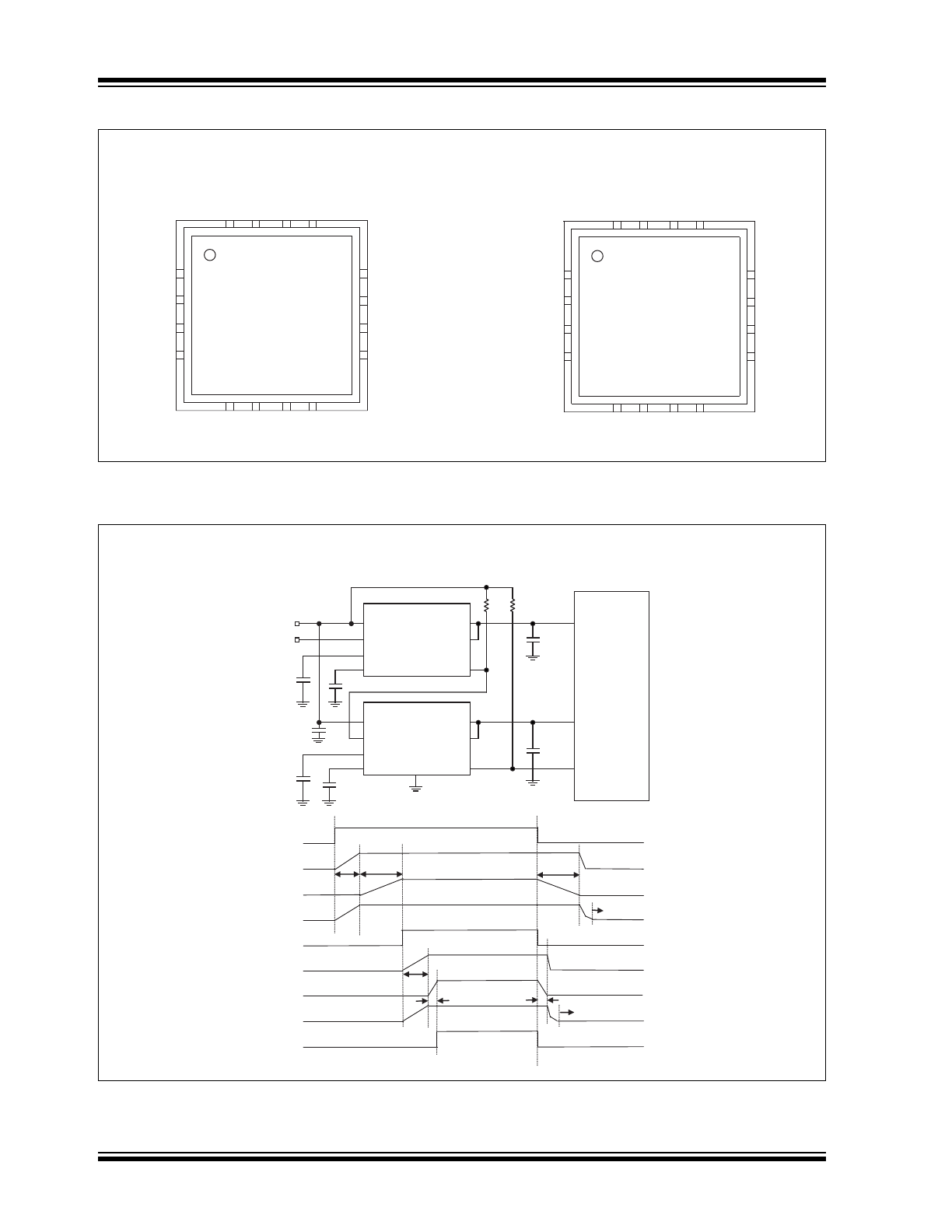
Package Types
Typical Application Circuits
MIC68400, F
IXED
V
OLTAGES
16-Lead QFN (ML)
MIC68400, A
DJ
. V
OLTAGES
16-Lead QFN (ML)
13
14
15
16
12
11
10
9
1
2
3
4
8
7
6
5
VIN
VIN
DELAY
RC
VOUT
VOUT
SNS
POR
VIN
VIN
NC
VOUT
EN
NC
GND
GND
13
14
15
16
12
11
10
9
1
2
3
4
8
7
6
5
VIN
VIN
DELAY
RC
VOUT
VOUT
ADJ
POR
VIN
VIN
NC
VOUT
EN
NC
GND
GND
MIC68400
Sequenced Dual Power Supply for I/O and Core Voltage of µProcessor
10μF
10μF
1nF
V
IN
= 3.3V
EN
IN1
OUT1
EN1
SNS1
RC1
DLY1
POR1
μProcessor
I/O
CORE
/RESET
47k
47k
10nF
0.7nF
0.6nF
MIC68400-1.8YML
U1
Master
MIC68400-1.5YML
U2
Slave
IN2
OUT2
EN2
SNS2
RC2
DLY2
GND
GND
POR2
0.1μF
U1.EN
U1.RC
U1.DLY
U1.OUT
U2.EN = U1.POR
U2.RC
U2.DLY
U2.OUT
U2.POR
U1.T
RC
U2.T
RC2
U1.T
DLY
U1.T
DLY
U2.T
DLY
U2.T
DLY
U1 Fully Shut Down
U2 Fully Shut Down
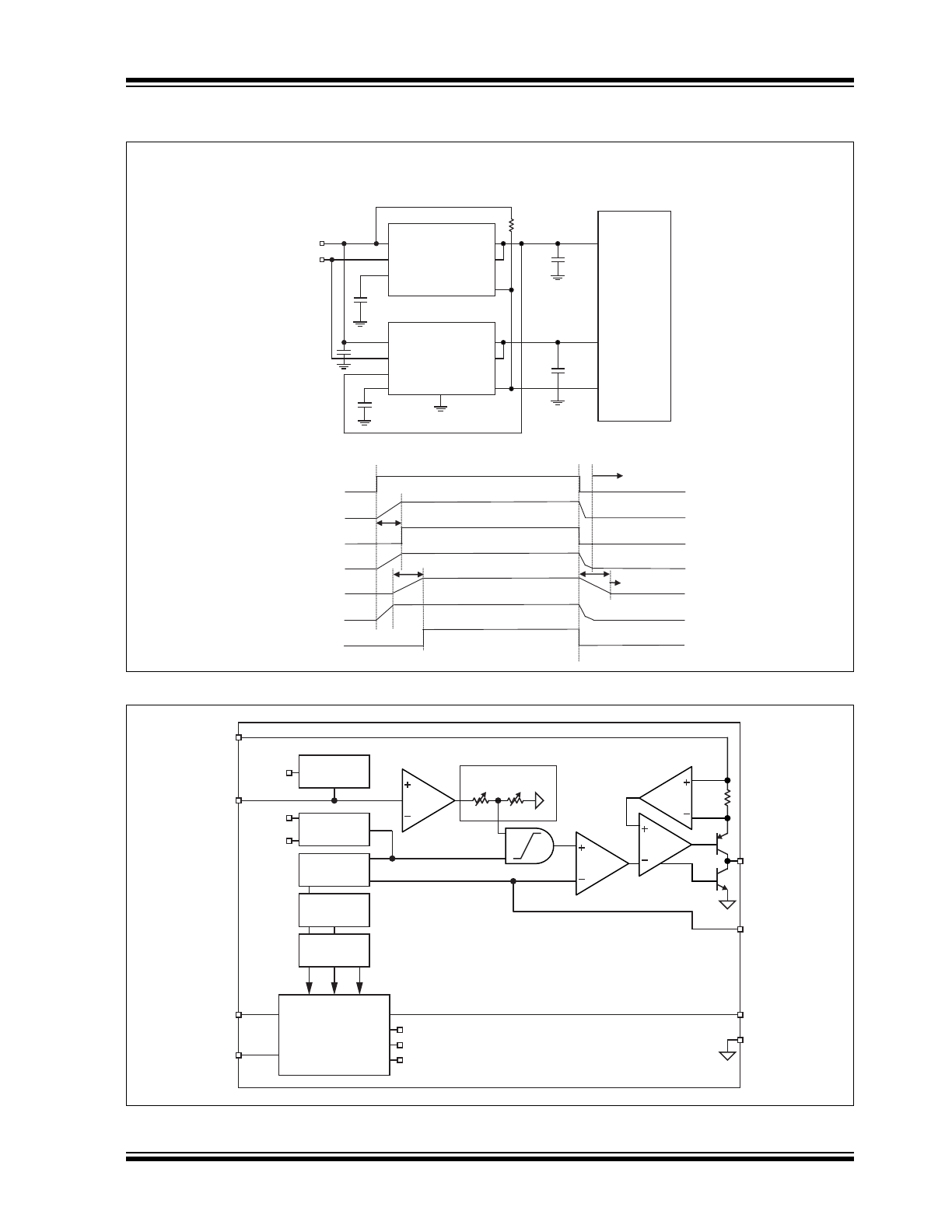
2017 Microchip Technology Inc.
DS20005824A-page 3
MIC68400
Typical Application Circuits (Continued)
Functional Block Diagram
10μF
10μF
10nF
V
IN
= 1.8V
EN
IN1
OUT1
EN1
RC1
DLY1
POR1
μProcessor
I/O
CORE
/RESET
47k
:
10nF
MIC68400-1.8YML
U1
Master
MIC68400-1.2YML
U2
Slave
IN2
OUT2
EN2
SNS2
SNS1
RC2
DLY2
GND
POR2
0.1μF
MIC68400
Tracking Dual Power Supply for I/O and Core Voltage of µProcessor
U1.EN = U2.EN
U1.RC
U1.DLY
U2.RC = U1.OUT
U2.DLY
U2.OUT
U1.POR = U.2POR
U1.T
RC
U2.T
DLY
U.2T
DLY
U1 Fully Shut Down
U2 Fully Shut Down
Bandgap
Reference
Output Error
Holdoff
Thermal
Shutdown
Low Voltage
Holdoff
Sequencing
Timer/Controller
BGStart
BGDis
Ramp
Control
RCDis
IN
RC
EN
DLY
BGStart: BandGap Startup
BGDis: BandGap Shutdown
RCDis: Ramp Control Discharge
GND
POR
SNS
OUT
RC
Buffer
Error
Amp
Current
Driver
Current
Limit
External on
Adjustable Part
AMP
MIN
MIC68400
DS20005824A-page 4
2017 Microchip Technology Inc.
1.0
ELECTRICAL CHARACTERISTICS
Absolute Maximum Ratings †
Supply Voltage (V
IN
)....................................................................................................................................................+6V
Enable Input Voltage (V
EN
) .........................................................................................................................................+6V
POR (V
POR
) ..................................................................................................................................................... V
IN
+ 0.3V
RC .................................................................................................................................................................... V
IN
+ 0.3V
Power Dissipation (P
D
), (
Note 1
)............................................................................................................Internally Limited
Operating Ratings ‡
Supply Voltage (V
IN
)................................................................................................................................ +1.65V to +5.5V
Enable Input Voltage (V
EN
) ................................................................................................................................ 0V to V
IN
Ramp Control (V
RC
) ....................................................................................................................................... 0V to +5.5V
†
Notice: Stresses above those listed under “Absolute Maximum Ratings” may cause permanent damage to the device.
This is a stress rating only and functional operation of the device at those or any other conditions above those indicated
in the operational sections of this specification is not intended. Exposure to maximum rating conditions for extended
periods may affect device reliability.
‡ Notice:
The device is not guaranteed to function outside its operating ratings.
Note 1:
The maximum allowable power dissipation of any T
A
(ambient temperature) is P
D(MAX)
= T
J(MAX)
– T
A
)/θ
JA
.
Exceeding the maximum allowable power dissipation will result in excessive die temperature, and the reg-
ulator will go into thermal shutdown.
TABLE 1-1:
ELECTRICAL CHARACTERISTICS
Electrical Characteristics:
T
A
= +25°C with V
IN
= V
OUT
+ 1V; V
EN
= V
IN
; I
OUT
= 10 mA; bold values indicate –40°C
≤ T
J
≤ +125°C, unless noted.
Note 1
Parameter
Symbol
Min.
Typ.
Max.
Units
Conditions
Output Voltage Accuracy
–2
—
2
%
10 mA < I
OUT
< I
L(MAX)
, V
OUT
+ 1 ≤
V
IN
≤ 5.5V
Feedback Voltage
V
FB
0.49
0.50
0.51
V
Adjustable version only
Feedback Current
I
FB
—
20
—
nA
Adjustable version only
Output Voltage Line
Regulation
—
0.06
0.5
%
V
IN
= V
OUT
+ 1V to 5.0V
Output Voltage Load
Regulation
—
0.5
1
%
I
L
= 10 mA to 3A
V
IN
– V
O
; Dropout Voltage
—
—
400
mV
I
L
= 1.5A
—
300
500
I
L
= 3.0A
—
360
800
I
L
= 4.0A
Ground Pin Current
I
GND
—
1.2
—
mA
I
L
= 10 mA
—
20
—
I
L
= 1.5A
—
55
—
I
L
= 3.0A
—
90
130
I
L
= 4.0A
Shutdown Current
I
SHDN
—
0.01
10
µA
V
EN
= 0V; V
OUT
= 0V
Current Limit
I
LIMIT
4.0
6.0
—
A
V
OUT
= 0V; V
IN
= 3.0V
Start-Up Time
t
SU
—
35
150
µs
V
EN
= V
IN
; CRC = Open
Enable Input
Enable Input Threshold
1
—
—
V
Regulator enable
—
—
0.2
Regulator shutdown
Enable Hysteresis
20
120
200
mV
—
2017 Microchip Technology Inc.
DS20005824A-page 5
MIC68400
Enable Input Current
—
0.02
—
µA
V
IL
≤ 0.2V (Regulator shutdown)
—
3
—
V
IH
≥ 1V (Regulator enable)
POR Output
POR Leakage Current
I
POR(LEAK)
—
—
1
µA
V
POR
= 5.5V; POR = High
—
—
2
V
POR(LO)
—
60
90
mV
Output Logic-Low Voltage
(undervoltage condition),
I
POR
= 1 mA
V
POR
7.5
10
12.5
%
V
OUT
Ramping Up, Threshold,
Percent of V
OUT
below nominal
10
12.5
15
V
OUT
Ramping Down, Threshold,
Percent of V
OUT
below nominal
—
3
—
Hysteresis
Delay Current
I
DELAY
0.7
1
1.3
µA
V
DELAY
= 0.75V
Delay Voltage (
Note 2
)
V
DELAY
1.185
1.235
1.285
V
V
POR
= High
Ramp Control
Ramp Control Current
I
RC
0.7
1
1.3
µA
V
RC
= 0.75V
Output Discharge Current
(
Note 3
)
I
DC(OUT)
25
45
70
mA
V
OUT
= 0.5V
NOM
, V
RAMP
=0V
Fixed Tracking Accuracy
(
Note 4
)
–50
25
100
mV
200 mV < V
RC
< V
TARGET
; Measure
(V
OUT
– V
RC
)
Adjustable Tracking Accuracy
(
Note 4
)
–10
15
50
mV
Measure (V
OUT
– V
RC
x
(V
TARGET
/500 mV))
Note 1:
Specification for packaged product only.
2:
Timer High Voltage along with Delay pin current (1 µA nom.) determines the delay per µF of capacitance.
Typical delay is 1.1 sec/µF.
3:
Discharge current is the current drawn from the output to ground to actively discharge the output capacitor
during the shutdown process.
4:
V
TARGET
is the output voltage of an adjustable with customer resistor divider installed between V
OUT
and
ADJ/SNS pin, or the rated output voltage of a fixed device.
TABLE 1-1:
ELECTRICAL CHARACTERISTICS (CONTINUED)
Electrical Characteristics:
T
A
= +25°C with V
IN
= V
OUT
+ 1V; V
EN
= V
IN
; I
OUT
= 10 mA; bold values indicate –40°C
≤ T
J
≤ +125°C, unless noted.
Note 1
Parameter
Symbol
Min.
Typ.
Max.
Units
Conditions

MIC68400
DS20005824A-page 6
2017 Microchip Technology Inc.
TEMPERATURE SPECIFICATIONS (
Note 1
)
Parameters
Sym.
Min.
Typ.
Max.
Units
Conditions
Temperature Ranges
Junction Temperature Range
T
J
–40
—
+125
°C
—
Storage Temperature Range
T
S
–65
—
+150
°C
—
Package Thermal Resistances
Thermal Resistance 16-LD 4x4 QFN
JA
—
30
—
°C/W
—
Note 1:
The maximum allowable power dissipation is a function of ambient temperature, the maximum allowable
junction temperature and the thermal resistance from junction to air (i.e., T
A
, T
J
,
JA
). Exceeding the
maximum allowable power dissipation will cause the device operating junction temperature to exceed the
maximum +125°C rating. Sustained junction temperatures above +125°C can impact the device reliability.
2017 Microchip Technology Inc.
DS20005824A-page 7
MIC68400
2.0
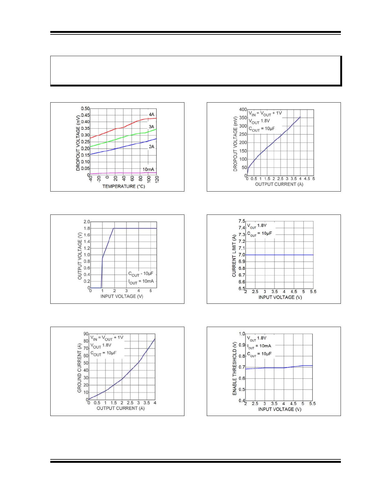
TYPICAL PERFORMANCE CURVES
FIGURE 2-1:
Dropout Voltage vs.
Temperature.
FIGURE 2-2:
Output Voltage vs. Input
Voltage.
FIGURE 2-3:
Ground Current vs. Output
Current.
FIGURE 2-4:
Dropout Voltage vs. Output
Current.
FIGURE 2-5:
Current Limit vs. Input
Voltage.
FIGURE 2-6:
Enable Threshold vs. Input
Voltage.
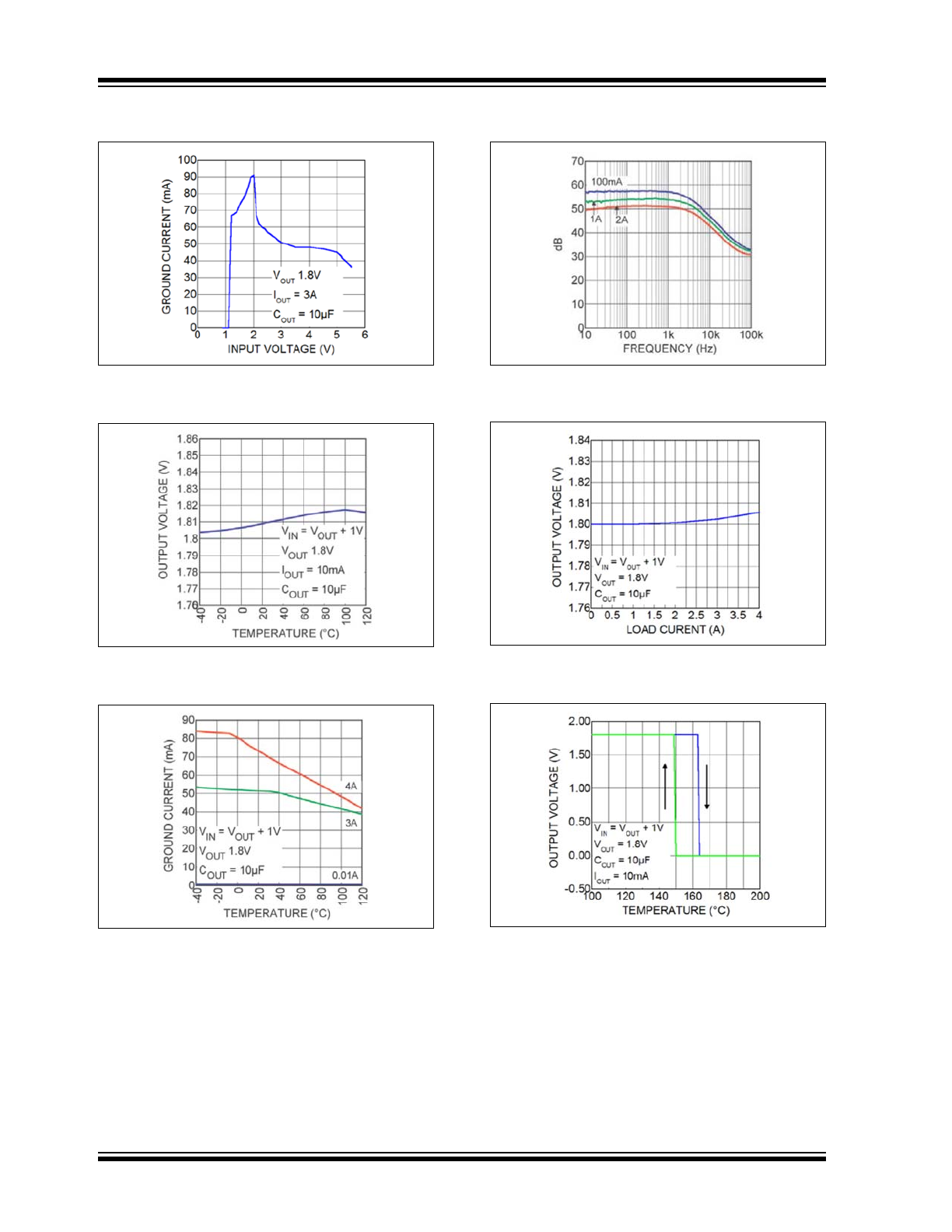
Note:
The graphs and tables provided following this note are a statistical summary based on a limited number of
samples and are provided for informational purposes only. The performance characteristics listed herein
are not tested or guaranteed. In some graphs or tables, the data presented may be outside the specified
operating range (e.g., outside specified power supply range) and therefore outside the warranted range.
MIC68400
DS20005824A-page 8
2017 Microchip Technology Inc.
FIGURE 2-7:
Ground Current vs. Input
Voltage.
FIGURE 2-8:
Output Voltage vs.
Temperature.
FIGURE 2-9:
Ground Current vs.
Temperature.
FIGURE 2-10:
Power Supply Rejection
Ratio.
FIGURE 2-11:
Load Regulation.
FIGURE 2-12:
Thermal Shutdown.
2017 Microchip Technology Inc.
DS20005824A-page 9
MIC68400
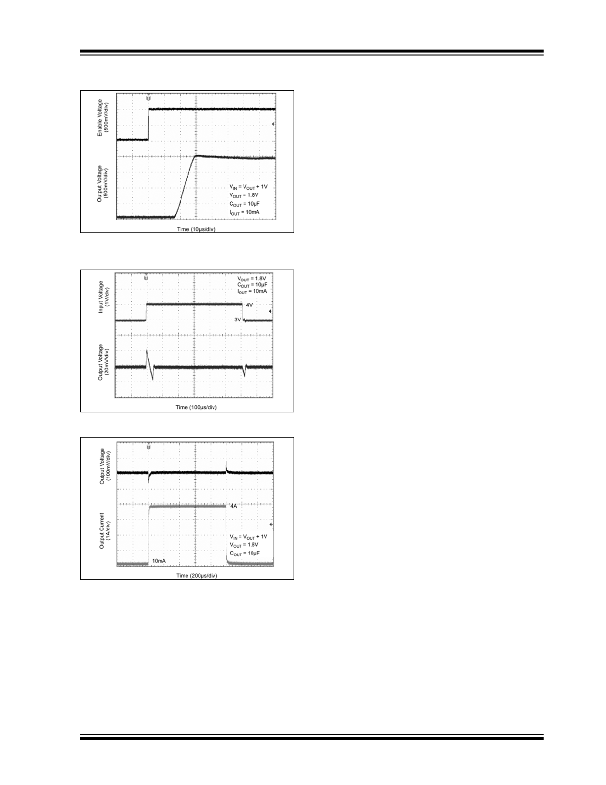
FIGURE 2-13:
Enable Turn-On
.
FIGURE 2-14:
Line Transient
.
FIGURE 2-15:
Load Transient.
MIC68400
DS20005824A-page 10
2017 Microchip Technology Inc.
3.0
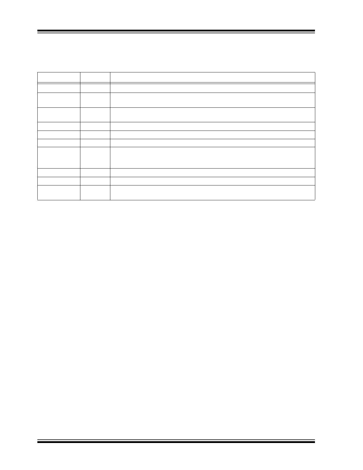
PIN DESCRIPTIONS
The descriptions of the pins are listed in
Table 3-1
.
TABLE 3-1:
PIN FUNCTION TABLE
Pin Number
Pin Name
Description
1, 2, 15, 16
V
IN
Input: Input voltage supply pin. Place a capacitor to ground to bypass the input supply.
3
DELAY
Delay: Capacitor to ground sets internal delay timer. Timer delays power-on reset
(POR) output at turn-on, and ramp down at turn-off.
4
RC
Ramp Control: May be voltage driven for tracking applications or a capacitor to ground
will set the slew rate of output voltage during start-up.
5
EN
Enable (Input): CMOS compatible input. Logic-high = enable, logic-low = shutdown.
6, 14
NC
Not internally connected.
7, 8, Tab
GND
Ground.
9
POR
Power-on Reset: Open-drain output device indicates when the output is in regulation.
High (open) means device is regulating within 10%. POR onset can be delayed using
a single capacitor from Delay to ground.
10 (Fixed)
SNS
Output Voltage Sense Pin: Connect directly to output pin.
10 (Adj.)
ADJ
Adjustable regulators: Feedback input. Connect to resistor voltage divider.
11, 12, 13
V
OUT
Output Voltage: Output of voltage regulator. Place capacitor to ground to bypass the
output voltage. Minimum load current is 100 µA. Nominal bypass capacitor is 10 µF.