
2015-2018 Microchip Technology Inc.
DS20005371D-page 1
47L04/47C04/47L16/47C16
Device Selection Table
Features
• 4 Kbit/16 Kbit SRAM with EEPROM Backup:
- Internally organized as 512 x 8 bits (47X04)
or 2,048 x 8 bits (47X16)
- Automatic Store to EEPROM array upon
power-down (using optional external
capacitor)
- Automatic Recall to SRAM array upon
power-up
- Hardware Store pin for manual Store
operations
- Software commands for initiating Store and
Recall operations
- Store time 8 ms maximum (47X04) or
25 ms maximum (47X16)
• Nonvolatile External Event Detect Flag
• High Reliability:
- Infinite read and write cycles to SRAM
- More than one million store cycles to
EEPROM
- Data retention: >200 years
- ESD protection: >4,000V
• High-Speed I
2
C Interface:
- Industry standard 100 kHz, 400 kHz and
1 MHz
- Zero cycle delay reads and writes
- Schmitt Trigger inputs for noise suppression
- Cascadable up to four devices
• Write Protection:
- Software write protection from 1/64 of SRAM
array to whole array
• Low-Power CMOS Technology:
- 200 µA active current typical
- 40 µA standby current (maximum)
• 8-Lead PDIP, SOIC, and TSSOP Packages
• Available Temperature Ranges:
Description
The Microchip Technology Inc.
47L04/47C04/47L16/47C16 (47XXX) is a 4/16 Kbit
SRAM with EEPROM backup. The device is organized
as 512 x 8 bits or 2,048 x 8 bits of memory, and
utilizes the I
2
C serial interface. The 47XXX provides
infinite read and write cycles to the SRAM while
EEPROM cells provide high-endurance nonvolatile
storage of data. With an external capacitor, SRAM
data is automatically transferred to the EEPROM upon
loss of power. Data can also be transferred manually
by using either the Hardware Store pin or software
control. Upon power-up, the EEPROM data is
automatically recalled to the SRAM. Recall can also
be initiated through software control.
The 47XXX is available in the 8-lead PDIP, SOIC, and
TSSOP packages.
Package Types
Part Number
Density (bits)
V
CC
Range
Max. Clock
Frequency
Temperature
Ranges
Packages
47L04
4K
2.7-3.6V
1 MHz
I, E
P, SN, ST
47C04
4K
4.5-5.5V
1 MHz
I, E
P, SN, ST
47L16
16K
2.7-3.6V
1 MHz
I, E
P, SN, ST
47C16
16K
4.5-5.5V
1 MHz
I, E
P, SN, ST
- Industrial (I):
-40°C to
+85°C
- Automotive (E):
-40°C to +125°C
V
CAP
A1
A2
V
SS
V
CC
HS
SCL
SDA
1
2
3
4
8
7
6
5
PDIP/SOIC/TSSOP
(8-pin)
4K/16K I
2
C Serial EERAM
47L04/47C04/47L16/47C16
DS20005371D-page 2
2015-2018 Microchip Technology Inc.
Typical Application Schematic Auto-Store Mode (ASE = 1)
Typical Application Schematic Manual Store Mode (ASE = 0)
Block Diagram
V
CC
V
CC
SCL
SDA
HS
V
SS
V
CC
1
4
5
7
6
8
PIC
®
MCU
47XXX
V
CAP
V
CC
C
VCAP
V
CC
V
CC
SCL
SDA
HS
V
SS
V
CC
1
4
5
7
6
8
PIC
®
MCU
47XXX
V
CAP
V
CC
Power
I
2
C Control Logic
Memory Address
and Data Control
Logic
Slave Address
V
CC
Control
Block
V
CAP
Decoder
EEPROM
512 x 8
RECALL
STORE
SDA
SCL
A2, A1
HS
2K x 8
SRAM
512 x 8
Status Register
2K x 8
2015-2018 Microchip Technology Inc.
DS20005371D-page 3
47L04/47C04/47L16/47C16
1.0
ELECTRICAL CHARACTERISTICS
1.1
Absolute Maximum Ratings
(†)
V
CC
.............................................................................................................................................................................6.5V
A1, A2, SDA, SCL, HS pins w.r.t. V
SS
.......................................................................................................... -0.6V to 6.5V
Storage temperature ...............................................................................................................................-65°C to +150°C
Ambient temperature under bias.............................................................................................................-40°C to +125°C
ESD protection on all pins........................................................................................................................................ ≥4 kV
† NOTICE
: Stresses above those listed under ‘Absolute Maximum Ratings’ may cause permanent damage to the
device. This is a stress rating only and functional operation of the device at those or any other conditions above those
indicated in the operational listings of this specification is not implied. Exposure to maximum rating conditions for an
extended period of time may affect device reliability.
TABLE 1-1:
DC CHARACTERISTICS
DC CHARACTERISTICS
47LXX:
V
CC
= 2.7V to 3.6V
47CXX:
V
CC
= 4.5V to 5.5V
Industrial (I):
T
A
= -40°C to +85°C
Automotive (E): T
A
= -40°C to +125°C
Param.
No.
Symbol
Characteristic
Min.
Typ.
Max.
Units
Conditions
D1
V
IH
High-Level Input Voltage
0.7
V
CC
—
V
CC
+1
V
D2
V
IL
Low-Level Input Voltage
-0.3
—
0.3
V
CC
V
D3
V
OL
Low-Level Output Voltage
—
—
0.4
V
I
OL
= 3.0 mA
D4
V
HYS
Hysteresis of Schmitt
Trigger Inputs (SDA, SCL
pins)
0.05
V
CC
—
—
V
Note 1
D5
I
LI
Input Leakage Current
(SDA, SCL pins)
—
—
±1
µA
V
IN
= V
SS
or V
CC
D6
I
LO
Output Leakage Current
(SDA pin)
—
—
±1
µA
V
OUT
= V
SS
or V
CC
D7
R
IN
Input Resistance to V
SS
(A1, A2, HS pins)
50
—
—
kΩ
V
IN
= V
IL
(max.)
750
—
—
kΩ
V
IN
= V
IH
(min.)
D8
C
INT
Internal Capacitance
(all inputs and outputs)
—
—
7
pF
T
A
= +25°C, F
REQ
= 1 MHz,
V
CC
= 5.5V (
Note 1
)
D9
I
CC
Active
Operating Current
—
200
400
µA
V
CC
= 5.5V, F
CLK
= 1 MHz
—
150
300
µA
V
CC
= 3.6V, F
CLK
= 1 MH
Z
D10
I
CC
Recall Recall Current (
Note 2
)
—
—
700
µA
V
CC
= 5.5V
—
300
500
µA
V
CC
= 3.6V
D11
I
CC
Store
Manual Store Current
(
Note 2
)
—
—
2500
µA
V
CC
= 5.5V
—
—
1500
µA
V
CC
= 3.6V
D12
I
CC
Auto-Store
Auto-Store Current
(
Notes 1
,
2
and
3
)
—
400
—
µA
V
CC
, V
CAP
= V
TRIP
(min.)
47CXX
—
300
—
µA
V
CC
, V
CAP
= V
TRIP
(min.)
47LXX
Note 1:
This parameter is periodically sampled and not 100% tested.
2:
Store and Recall currents are specified as an average current across the entire operation.
3:
C
VCAP
required when Auto-Store is enabled (ASE = 1).
47L04/47C04/47L16/47C16
DS20005371D-page 4
2015-2018 Microchip Technology Inc.
D13
I
CC
Status
Write
Status Write Current
—
—
2500
µA
V
CC
= 5.5V
—
—
1500
µA
V
CC
= 3.6V
D14
I
CCS
Standby Current
—
—
40
µA
SCL, SDA, V
CAP
, V
CC
= 5.5V
—
—
40
µA
SCL, SDA, V
CAP
, V
CC
= 3.6V
D15
V
TRIP
Auto-Store/Auto-Recall
Trip Voltage
4.0
—
4.4
V
47CXX
2.4
—
2.6
V
47LXX
D16
V
POR
Power-On Reset Voltage
—
1.1
—
V
D17
C
B
Bus Capacitance
—
—
400
pF
D18
C
VCAP
Auto-Store Capacitance
(
Notes 1
and
3
)
3.5
4.7
—
µF
47C04
5
6.8
—
µF
47C16
5
6.8
—
µF
47L04
8
10
—
µF
47L16
TABLE 1-1:
DC CHARACTERISTICS (CONTINUED)
DC CHARACTERISTICS
47LXX:
V
CC
= 2.7V to 3.6V
47CXX:
V
CC
= 4.5V to 5.5V
Industrial (I):
T
A
= -40°C to +85°C
Automotive (E): T
A
= -40°C to +125°C
Param.
No.
Symbol
Characteristic
Min.
Typ.
Max.
Units
Conditions
Note 1:
This parameter is periodically sampled and not 100% tested.
2:
Store and Recall currents are specified as an average current across the entire operation.
3:
C
VCAP
required when Auto-Store is enabled (ASE = 1).
2015-2018 Microchip Technology Inc.
DS20005371D-page 5
47L04/47C04/47L16/47C16
TABLE 1-2:
AC CHARACTERISTICS
AC CHARACTERISTICS
47LXX:
V
CC
= 2.7V to 3.6V
47CXX:
V
CC
= 4.5V to 5.5V
Industrial (I):
T
AMB
= -40°C to +85°C
Automotive (E):
T
AMB
= -40°C to +125°C
Param.
No.
Symbol
Characteristic
Min.
Max.
Units
Conditions
1
F
CLK
Clock Frequency
—
1000
kHz
2
T
HIGH
Clock High Time
500
—
ns
3
T
LOW
Clock Low Time
500
—
ns
4
T
R
SDA and SCL Input Rise
Time
—
300
ns
Note 1
5
T
F
SDA and SCL Input Fall
Time
—
300
ns
Note 1
6
T
HD
:
STA
Start Condition Hold Time
250
—
ns
7
T
SU
:
STA
Start Condition Setup
Time
250
—
ns
8
T
HD
:
DAT
Data Input Hold Time
0
—
ns
9
T
SU
:
DAT
Data Input Setup Time
100
—
ns
10
T
SU
:
STO
Stop Condition Setup
Time
250
—
ns
11
T
AA
Output Valid from Clock
—
400
ns
12
T
BUF
Bus Free Time: Bus time
must be free before a new
transmission can start
500
—
ns
13
T
SP
Input Filter Spike
Suppression (SDA, SCL
and HS pins)
—
50
ns
Note 1
14
T
HSPW
Hardware Store Pulse
Width
150
—
ns
15
T
RECALL
Recall Operation Duration
—
5
ms
47X16
—
2
ms
47X04
16
T
STORE
Store Operation Duration
—
25
ms
47X16
—
8
ms
47X04
17
T
WC
STATUS Register Write
Cycle Time
—
1
ms
18
T
VRISE
V
CC
Rise Rate
70
—
µs/V
Note 1
19
Tv
FALL
V
CC
Fall Rate
70
—
µs/V
Note 1
20
EEPROM Endurance
1,000,000
—
Store
cycles
+25°C, V
CC
= 5.5V
(
Notes 1
and
2
)
Note 1:
This parameter is not tested but ensured by characterization.
2:
For endurance estimates in a specific application, please consult the Total Endurance Model which can
be obtained on Microchip’s website at www.microchip.com.
47L04/47C04/47L16/47C16
DS20005371D-page 6
2015-2018 Microchip Technology Inc.
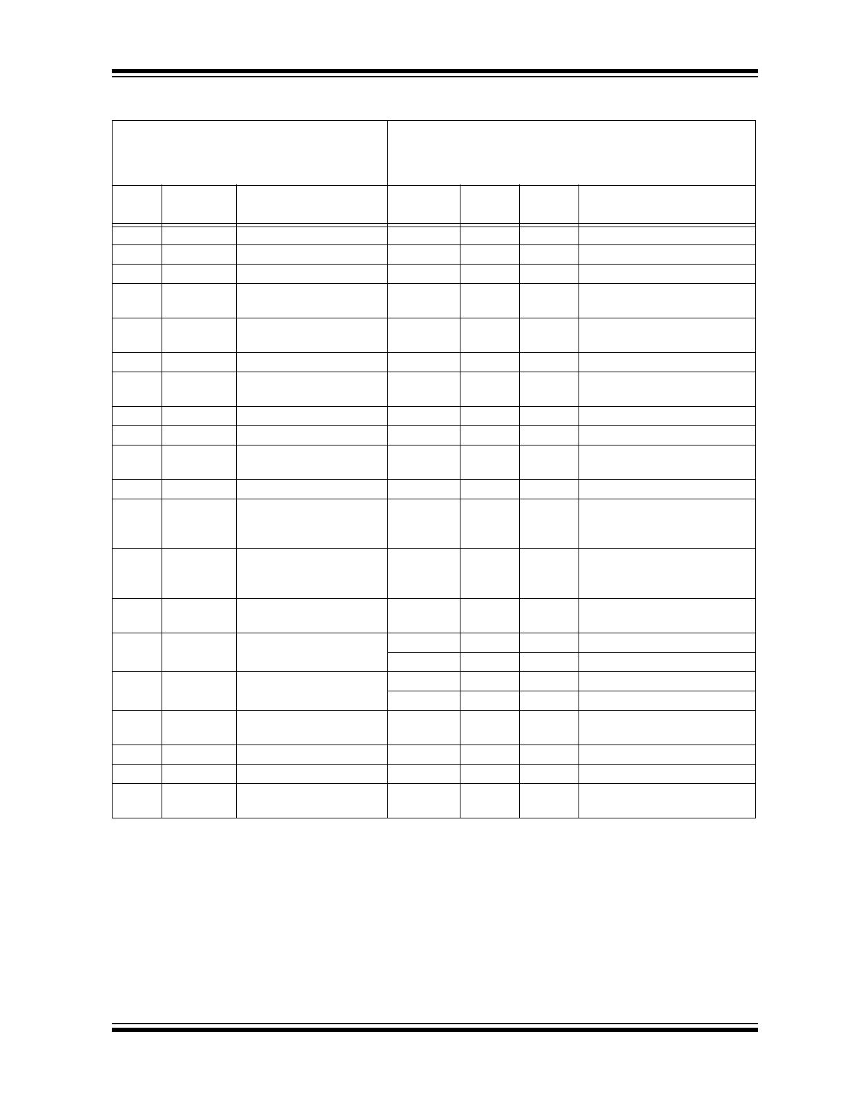
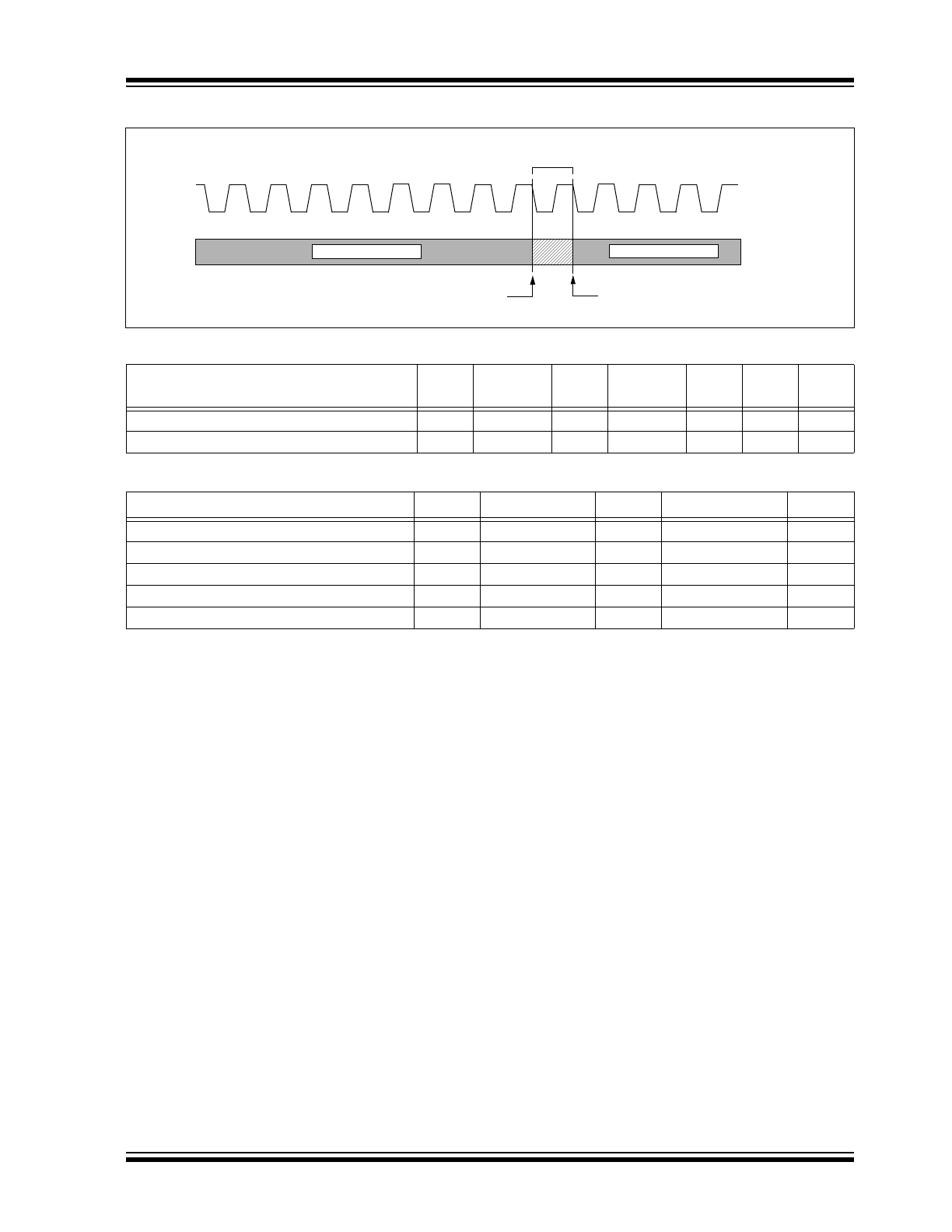
FIGURE 1-1:
BUS TIMING DATA
FIGURE 1-2:
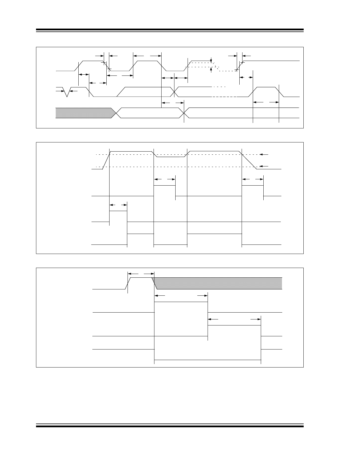
AUTO-STORE/AUTO-RECALL TIMING DATA
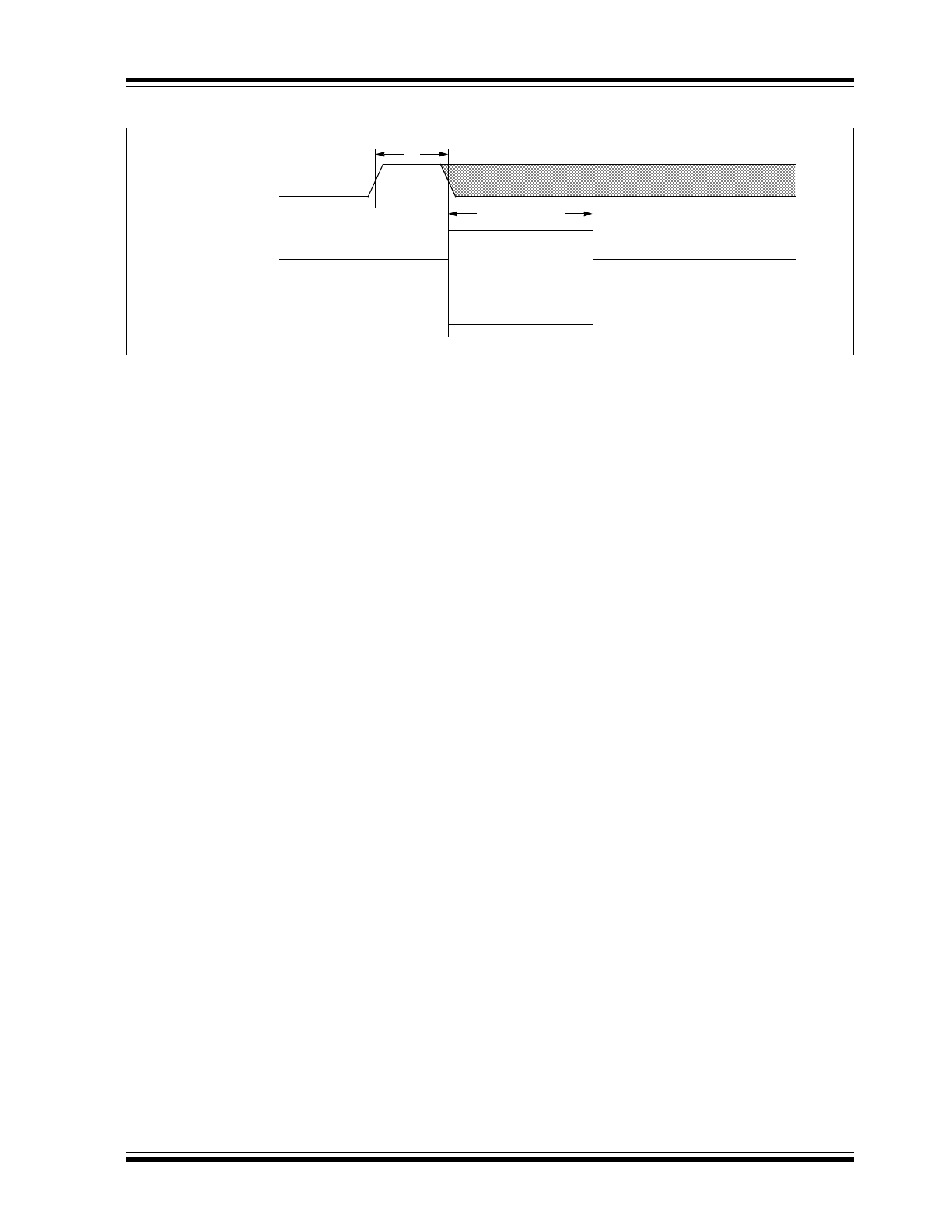
FIGURE 1-3:
HARDWARE STORE TIMING DATA (WITH AM = 1)
SCL
SDA
IN
SDA
OUT
5
7
6
13
3
2
8
9
11
D4
4
10
12
Auto-Store
Auto-Recall
15
16
16
D15
V
CAP
Device Access
Enabled
D16
Device Access
Enabled
STATUS Register
17
HS Pin
14
Write Cycle
Hardware Store
16
Operation
2015-2018 Microchip Technology Inc.
DS20005371D-page 7
47L04/47C04/47L16/47C16
FIGURE 1-4:
HARDWARE STORE TIMING DATA (WITH AM = 0)
Device Access
Enabled
STATUS Register
17
HS Pin
14
Write Cycle
47L04/47C04/47L16/47C16
DS20005371D-page 8
2015-2018 Microchip Technology Inc.
2.0
FUNCTIONAL DESCRIPTION
2.0.1
PRINCIPLES OF OPERATION
The 47XXX is a 4/16 Kbit serial EERAM designed to
support a bidirectional two-wire bus and data
transmission protocol (I
2
C). A device that sends data
onto the bus is defined as transmitter, and a device
receiving data is defined as receiver. The bus has to
be controlled by a master device which generates the
Start and Stop conditions, while the 47XXX works as
slave. Both master and slave can operate as
transmitter or receiver, but the master device
determines which mode is active.
2.1
Bus Characteristics
2.1.1
SERIAL INTERFACE
The following bus protocol has been defined:
• Data transfer may be initiated only when the bus
is not busy.
• During data transfer, the data line must remain
stable whenever the clock line is high. Changes in
the data line while the clock line is high will be
interpreted as a Start or Stop condition.
Accordingly, the following bus conditions have been
defined (
Figure 2-1
).
2.1.1.1
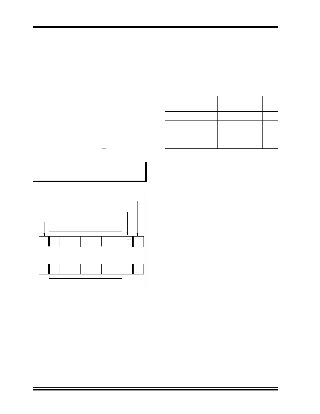
Bus Not Busy (A)
Both data and clock lines remain high.
2.1.1.2
Start Data Transfer (B)
A high-to-low transition of the SDA line while the clock
(SCL) is high determines a Start condition. All
commands must be preceded by a Start condition.
2.1.1.3
Stop Data Transfer (C)
A low-to-high transition of the SDA line while the clock
(SCL) is high determines a Stop condition. All
operations must end with a Stop condition.
2.1.1.4
Data Valid (D)
The state of the data line represents valid data when,
after a Start condition, the data line is stable for the
duration of the high period of the clock signal.
The data on the line must be changed during the low
period of the clock signal. There is one bit of data per
clock pulse.
Each data transfer is initiated with a Start condition and
terminated with a Stop condition. The number of the
data bytes transferred between the Start and Stop con-
ditions is determined by the master device.
2.1.1.5
Acknowledge
Each receiving device, when addressed, is obliged to
generate an Acknowledge signal after the reception of
each byte. The master device must generate an extra
clock pulse which is associated with this Acknowledge
bit.
A device that Acknowledges must pull down the SDA
line during the Acknowledge clock pulse in such a way
that the SDA line is stable low during the high period of
the Acknowledge related clock pulse. Of course, setup
and hold times must be taken into account. During
reads, a master must signal an end of data to the slave
by NOT generating an Acknowledge bit on the last byte
that has been clocked out of the slave. In this case, the
slave (47XXX) will leave the data line high to enable the
master to generate the Stop Condition.
There are situations where the 47XXX will NOT
generate an Acknowledge bit in order to signal that an
error has occurred.
Table 2-1
and
Table 2-2
summarize
these situations.
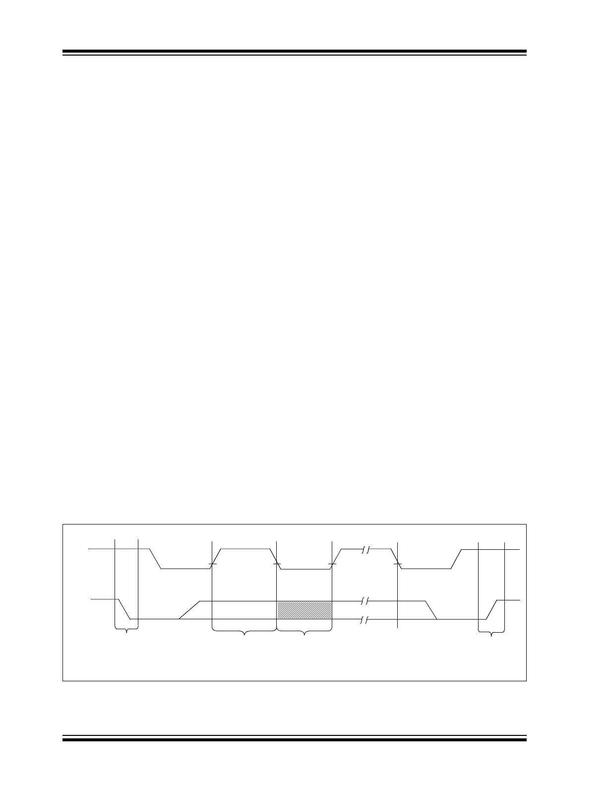
FIGURE 2-1:
DATA TRANSFER SEQUENCE ON THE SERIAL BUS
Address or
Acknowledge
Valid
Data
Allowed
to Change
Stop
Condition
Start
Condition
SCL
SDA
(A)
(B)
(D)
(D)
(C)
(A)
2015-2018 Microchip Technology Inc.
DS20005371D-page 9
47L04/47C04/47L16/47C16
FIGURE 2-2:
ACKNOWLEDGE TIMING
TABLE 2-1:
ACKNOWLEDGE TABLE FOR SRAM WRITES
Instruction
ACK
Address
MSB
ACK
Address
LSB
ACK
Data
Byte
ACK
SRAM Write in Unprotected Block
ACK
Address
ACK
Address
ACK
Data
ACK
SRAM Write in Protected Block
ACK
Address
ACK
Address
ACK
Data
NoACK
TABLE 2-2:
ACKNOWLEDGE TABLE FOR CONTROL REGISTER WRITES
Instruction
ACK
Address
ACK
Data Byte
ACK
STATUS Register Write
ACK
00h
ACK
Data
ACK
Software Store Command
ACK
55h
ACK
33h
ACK
Software Recall Command
ACK
55h
ACK
DDh
ACK
Write Invalid Value to COMMAND Register
ACK
55h
ACK
Invalid Command
NoACK
Write to Invalid Register Address
ACK
Invalid Address
NoACK
Don’t Care
NoACK
SCL
9
8
7
6
5
4
3
2
1
1
2
3
Transmitter must release the SDA line at this point
allowing the Receiver to pull the SDA line low to
acknowledge the previous eight bits of data.
Receiver must release the SDA line at this point
so the Transmitter can continue sending data.
Data from transmitter
Data from transmitter
SDA
Acknowledge
Bit
47L04/47C04/47L16/47C16
DS20005371D-page 10
2015-2018 Microchip Technology Inc.
2.2
Device Addressing
The control byte is the first byte received following the
Start condition from the master device (
Figure 2-3
).
The control byte begins with a 4-bit operation code.
The next two bits are the user-configurable Chip
Select bits: A2 and A1. The next bit is a non-configu-
rable Chip Select bit that must always be set to ‘0’.
The Chip Select bits A2 and A1 in the control byte
must match the logic levels on the corresponding A2
and A1 pins for the device to respond.
The last bit of the control byte defines the operation to
be performed. When set to a ‘1’ a read operation is
selected, and when set to a ‘0’ a write operation is
selected.
The combination of the 4-bit operation code and the
three Chip Select bits is called the slave address.
Upon receiving a valid slave address, the slave device
outputs an acknowledge signal on the SDA line.
Depending on the state of the R/W bit, the 47XXX will
select a read or a write operation.
FIGURE 2-3:
CONTROL BYTE FORMAT
The 47XXX is divided into two functional units: the
SRAM array and the Control registers.
Section 2.3
“SRAM Array”
describes the functionality for the
SRAM array and
Section 2.4 “Control Registers”
describes the Control registers.
The 4-bit op code in the control byte determines which
unit will be accessed during an operation.
Table 2-3
shows the standard control bytes used by the 47XXX.
Note:
When V
CAP
is below V
TRIP
, the 47XXX
cannot be accessed and will not
acknowledge any commands.
1
0
1
0
A2
A1
0
S
ACK
R/W
Op Code
Chip Select
Bits
Slave Address
Acknowledge Bit
Start Bit
Read/Write Bit
0
0
1
1
A2
A1
0
S
ACK
R/W
OR
TABLE 2-3:
CONTROL BYTES
Operation
Op
Code
Chip
Select
R/W
Bit
SRAM Read
1010
A2 A1 0
1
SRAM Write
1010
A2 A1 0
0
Control Register Read
0011
A2 A1 0
1
Control Register Write
0011
A2 A1 0
0